the Creative Commons Attribution 4.0 License.
the Creative Commons Attribution 4.0 License.
Development of an Internet of Things (IoT) embedded open-source gamma-ray detector using CMOS image sensor technology
Damián Leonel Corzi
Jose Lipovetzky
Mariano Gómez Berisso
This work presents a portable gamma-ray dosimeter which uses as a detector a CMOS image sensor mounted on a compact low-cost Internet of Things (IoT)-compatible ESP32-CAM embedded board. The detector uses simple, physics-based processing algorithms to allow for particle detection using CMOS image sensors on boards with limited processing capabilities. The detector enables real-time acquisition and processing, achieving nearly 100 % live measurement time, and the measurement results can be accessed from any device connected to the Wi-Fi network. A dose–event relation of (80 ± 5) nSv per event, calibrated with a Cs-137 gamma source, is suitable for cost-effective environmental radiation monitoring, personal dosimetry, or education purposes. The firmware is released as open-source, making it accessible for public use.
- Article
(2144 KB) - Full-text XML
- BibTeX
- EndNote
Ionizing radiation detection with portable sensors is important in dosimetry, radiation protection, environmental monitoring in facilities, and homeland security (Brown et al., 2016; Walsh et al., 2019; Fujibuchi et al., 2019; Dhanekar and Rangra, 2021). If the sensors are low-cost and have wireless connectivity, they can be used as portable or wearable dosimeters for personnel exposed in their workplace, to build large networks of detectors for area monitoring, or in science education to conduct simple experiments with low-activity elements.
Lowering their cost allows for, e.g., the democratization of environmental radiation measurements. An example of a low-cost detector with a significant social impact was the Geiger-based bGeigie Nano, which enabled independent, citizen-driven, radiation monitoring following the Fukushima plant accident (Walsh et al., 2019). Lower costs would enable not only broader utilization, but also educational kits.
The improvement in commercial off-the-shelf (COTS) CMOS image sensor (CIS) technology in recent years has reduced the sensor costs and enhanced its performance and complexity. Since CISs are also sensitive to ionizing radiation, e.g., gamma or X-rays, these advantages allow for their use as ionizing radiation detectors (Pérez et al., 2016; Shoulong et al., 2017; Lin et al., 2024).
Typically, radiation detection with CIS involves processing the sensor's raw data on a personal computer with sufficient computational power and memory to enable real-time results. Moreover, not only does the immediate image need to be analyzed, but old data are also needed to mitigate the effect of dark noise and defective pixels, which are dependent on temperature variations and radiation-induced aging (Bessia et al., 2018).
Unlike most previous work including smartphone-based detectors (Johary et al., 2021), which rely on image post-processing using standard computing resources, our approach implements a novel real-time embedded algorithm for radiation detection with minimal computational overhead. This includes a defective pixel masking method to mitigate dark noise specifically designed for memory-limited environments, allowing for the proper operation of the detector on a portable low-computational-power board.
Furthermore, the use of a low-cost ESP32-CAM board as a fully integrated platform with Internet of Things (IoT) capabilities provides the developed system with connectivity options that make it ideal for generating distributed sensor networks or accessing measured information remotely from any connected device, such as computers or smartphones, which constitutes a novel combination of hardware and firmware for portable dosimetry.
The remainder of the paper is structured as follows: the next section presents the device characteristics and the embedded algorithms used for particle detection, including the description of the proposed detection method. The result section presents the system response to radioactive sources, and the final section summarizes the main conclusions.
The board in which the new detection strategy is embedded to build a portable and low-cost detector is ESP32-CAM, with a cost below USD 10. It integrates an ESP32-S microcontroller and an OV2640 CIS. The difficulty of using it is that with the limited memory and processing power available to save and process raw images, it is impossible to perform real-time analysis, reducing measurement live time. For this reason, the approach used in detection involves a pixel-by-pixel analysis of the image.
2.1 Detector hardware
The OV2640 mounted on the ESP32-CAM board is the CIS used as a detector. It is a color UXGA CIS with a pixel pitch of 2.2 × 2.2 µm2, sensitivity of 0.6 V Lx−1 s−1, signal-to-noise ratio of 40 dB, dark current of 15 mV s−1, and well capacity of 12 ke−. The sensor was covered with a thin aluminum foil to obscure it, shielding visible light but generating negligible attenuation for high-energy photons.
The ESP32-S microcontroller is a 32-bit dual-core CPU running at 240 MHz with a built-in 520 KB SRAM. The board has Wi-Fi and Bluetooth connectivity, allowing IoT systems to transmit the measurement results. The board integrates an external 4 MB PSRAM memory and voltage regulators in a compact form factor with a size of 27 mm × 40.5 mm × 4.5 mm.
Finally, Fig. 1 shows the platform with the sensor covered with the aluminum tape. The board was mounted on an ad hoc shield used for programming and debugging the microcontroller via a serial protocol, but the system can be programmed using any compatible USB–UART bridge.
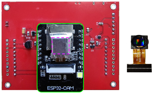
Figure 1ESP32-CAM board (framed by a green solid line) with the OV2640 sensor shielded by aluminum foil (framed by a magenta dashed line) mounted on the ad hoc programmer (red board). The disconnected OV2640 sensor without the lens and aluminum shield is shown on the right, allowing for a direct view of the CMOS integrated circuits.
2.2 Algorithm for real-time particle detection
The detection uses the signal generated by radiation on the CIS. When a gamma ray – or any other high-energy particle – interacts with the CIS, electron–hole pairs are generated in the pixels photodiodes. The charge generated appears as bright spots in the image, as shown in Fig. 2. Each spot, caused by a single particle, consists of a cluster of pixels with a signal much higher than the dark noise (Pérez et al., 2016). The size of the cluster of bright pixels depends on the secondary particles involved in the interaction process (Bagatin and Gerardin, 2018).
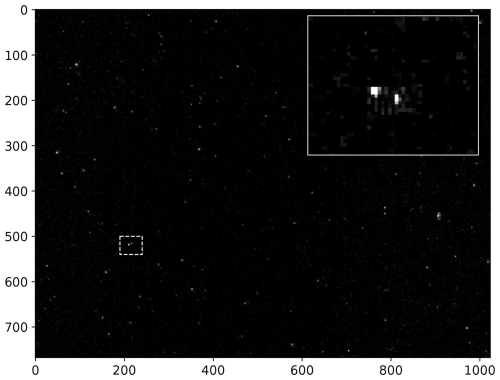
Figure 2Detected events generated by 0.6617 MeV photons using the OV2640 imager set to XGA resolution. In the inset, it is possible to appreciate the presence of two events in greater detail.
In this way, the firmware configures the sensor; reads the pixel signals; identifies defective pixels with high dark currents, which can generate false positives; and transmits the calibrated results. The code was based on the ESP32 Camera Driver project (ESP, 2023), which provides a large catalog of compatible cameras. Following the same approach, our code is available on a public repository (Corzi et al., 2025).
2.3 Sensor configuration
Many CISs are typically configured by enabling features to enhance the visual quality of the image. However, to accurately measure the charge generated by an ionizing particle, the bright spots in Fig. 2, these features need to be disabled. Sensor's built-in automatic gain control and white balance (Pérez et al., 2016) were disabled since they would not allow for a linear response between the signal and the digital analog-to-digital unit output. The sensor gain was set to its minimum value to reduce pixel saturation and extend the measurement range. The automatic exposure time control was disabled, and the exposure time was manually set to the maximum configurable value of 0.64 s to reduce dead time and maximize the detector measurement duty cycle. As is shown below, even with the maximum exposure time, the dark current remains low enough to allow for the identification of radiation-induced charge in the pixels.
Most modern sensors provide automatic white pixel correction, which identifies isolated pixels with a high value, replacing the measured signal with an average of neighboring pixels to avoid white pixels in a picture. However, for radiation detectors, this feature would cause false negatives for single-pixel events, which can occur at low X-ray energy levels (Pérez et al., 2020). Thus, the built-in defective pixel correction was disabled, and an ad hoc pixel correction procedure was created as explained below.
2.4 Data acquisition
Internally, video data are continuously transferred with an i2s protocol, pixel by pixel, from the sensor to the DMA microprocessor and copied into memory buffers. Taking advantage of the dual-core CPU and FreeRTOS, the buffers are read and analyzed by a task that runs with the highest priority in the secondary core. For this reason and because of the long exposure time set, the interval between new data arrivals is large enough to ensure that signals are processed before the next set of data comes in. This results in negligible dead time between measurements, allowing the sensor to detect particles almost continuously, maximizing whole detection efficiency.
Instead of saving entire images and subsequently searching for events within them, the strategy is to identify pixels above a threshold in real time. The pixel intensity is stored by incrementing the value in a 256-position vector that functions as a histogram of the values and reduces the amount of data from a 1600×1200 matrix to a 256-wide vector. The blue plot of Fig. 3 shows the histogram of all the dark sensor's pixel intensities from 1000 frames. A “0” represents a dark pixel, and a “255” represents the brightest pixels in an image.
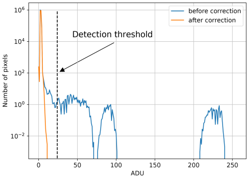
Figure 3Histograms of the number of pixels with a given arbitrary digital unit (ADU) signal per image obtained from 1000 frames. Blue and orange histograms correspond to before and after the application of the pixel discard process, respectively. The presence of pixels with a high dark current is not observed in the histogram generated after the discard process.
2.5 Defective pixel identification and discard
Some defective pixels in the CIS may exhibit large dark currents usually due to displacement damage (Bessia et al., 2018), which can introduce false positives being confused with ionizing particles. For instance, Fig. 3 shows the histogram of pixel intensity obtained with the CIS obscured and not irradiated in blue. Most pixels have low dark signals below 10 ADU, and only a few defective pixels have large values. These few defective pixels need to be ignored during the detection process, as is done with the pixel masking in the Medipix monolithic detector (Llopart et al., 2009). Since these pixels also exhibit a high amount of random telegraphic noise (Durnez et al., 2016), subtracting the average value can also be insufficient to ensure low false-positive rates.
To identify pixels with a high dark current, dark images are obtained upon device power. Pixels with repeated readings above a defective pixel threshold DEFT are identified as damaged, and their addresses are saved in a vector and then ignored during detection. Since the dark current increases with temperature – and the sensor warms up during use – DEFT is automatically calculated after taking 500 frames to allow for thermal stabilization. Figure 3 also shows the histogram after applying the correction, where pixels with a high dark current were successfully removed.
Over the sensor's operational lifespan, eventual exposure to high-energy neutrons or ions in the irradiation environment can lead to an increased number of defective pixels. Therefore, the vector size is set to a sufficiently large value to fit potential additions of discarded pixels – approximately 10 000 addresses, representing 0.5 % of the OV2640 CIS.
2.6 Event detection and calibration
The event detection is performed by counting the number of bright pixels with a signal higher than a detection threshold DETT, which needs to be set. If DETT is too low, false positives may occur due to dark noise. If DETT is too high, many events will not be counted, and the sensitivity of the device will be lower. For this reason, DETT is defined after applying the discard process to 10 digital numbers above the last non-zero channel of 1000 frames, as depicted in Fig. 3. This effectively minimizes the probability of false positives. Since the signal generated by radiation adds to the noise, this ensures constant detection efficiency.
The average number of pixels above the DETT is proportional to the radiation dose absorbed during the exposure time. To calibrate the detector as a dosimeter, a calibration constant is obtained by dividing the measured dose by the number of pixels that are above DETT. Since each detected event typically activates multiple adjacent pixels, as shown in Fig. 2, the number of events can be estimated by dividing the total counted pixels that are above the threshold by the average number of pixels activated per event.
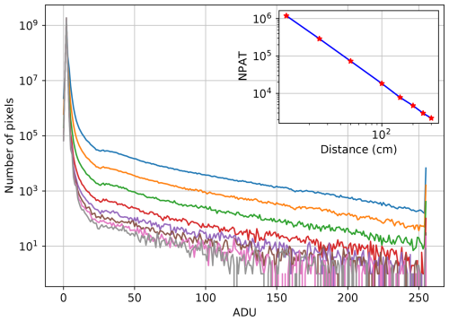
Figure 4Histograms obtained from 1000 frames varying the distance – from top to bottom at 12, 50, 100, 150, 200, 250, and 300 cm – between the detector and the gamma source. The inset shows the inverse-square law expected response, where the vertical axis represents NPAT, the number of pixels above DETT.
The detector was calibrated using a 0.54 Ci Cs-137m gamma source with a dose rate directly provided by the supplier in sieverts (Sv). Measurements were performed at multiple source-to-detector distances using a movable platform and were cross-validated against a calibrated reference detector. Figure 4 shows the histograms obtained irradiating the sensor, and the inset shows that the number of pixels above DETT follows the expected inverse-square law.
It is important to note that while the detector is sensitive to ionizing events in general, its response to alpha and beta radiation is limited by the sensor's shielding. The thin aluminum foil attenuates low-energy beta particles and completely blocks alpha particles. Therefore, the detector is primarily sensitive to gamma radiation and does not require additional calibration for low-energy charged particles. Although the dose rate is expressed in units of sieverts per hour, the weighting factor between the absorbed dose and equivalent dose is equal to 1 for X-rays and gamma rays.
In addition, the device's operation was verified using calibration sources of different radioisotopes, including some that emit beta rays during their decay chain, which allowed for the verification of the appropriate operation of the detector. For each measurement, the dose absorbed by the sensor was estimated considering the irradiation geometry and compared with a calibrated Geiger–Müller detector.
2.7 Data transmission
Once the dose rate is calculated, the results are published. Taking advantage of the IoT capabilities of the board, an embedded website was developed to display the measurement results in a web browser. The site was implemented using Google Charts to plot the estimated dose rate, updating information periodically asynchronously. The browser requests the number of pixels that are above DETT using plain text and uses the value to calculate the dose rate. Performing this calculation directly in the web browser reduces the processor usage and the amount of data sent over Wi-Fi. Additionally, any device on the same network can request data via HTTP, allowing for the development of low-cost networks of distributed wireless sensors for dose estimation. The results are also sent to the serial port for debugging.
Using the Cs-137 source, the calibration constant was (24.6±1.4) nSv per pixel. Measuring the average number of pixels above DETT per event, which is 3.25 pixels, the dose–event relation was estimated to be (80±5) nSv/event. Considering the calibration constant and accepting a statistical deviation of 10 % in 20 s exposure time, the system can measure dose rates with a resolution of down to 28 µSv min−1.
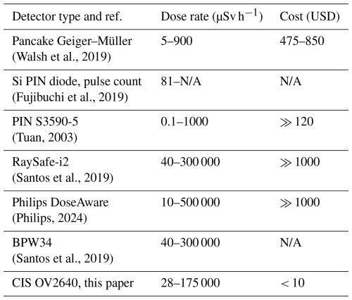
To compare the dose rate ranges of the approach, we present in Table 1 the performance of different state-of-the-art detectors based on different detection technologies. Our work compares to other silicon-detector-based and even to some Geiger–Müller detectors in dose rate measurement at a low cost. Although environmental monitoring for the general public requires a higher dose rate resolution (IEC, 2007), the system's resolution is sufficient for most applications involving educational and didactic purposes.
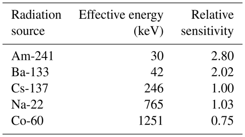
Walsh et al., 2019Fujibuchi et al., 2019Tuan, 2003Santos et al., 2019Philips, 2024Santos et al., 2019The detector sensitivity, defined as the number of events per dose, was calculated for the different radioisotopes using the Cs-137 source as a reference and expressed in Table 2. It is possible to appreciate that the efficiency of the detector decreases as the mean energy of the detected photons increases, which is reasonable when considering the dependence of the mass energy absorption coefficient on energy. The effective energy value was calculated by considering the relative intensity of gamma and X-ray photons and the attenuation generated by the shielding placed to block beta particles.
Analyzing the compilation results provided by the ESP-IDF Development Framework version 1.8.1, the compiled image used 40.0 % of DRAM memory; 86.2 % of IRAM memory; and 784 169 bytes of external FLASH memory, which corresponds to 18.19 %. Furthermore, the acquisition and transmission tasks were able to operate in parallel without causing data loss, ensuring that new functionality can be added to the system in future development.
With the sensor used to capture the histogram in Fig. 3, the automatic pixel discard routines identified 120 defective pixels which were later not taken into account in the detection process. In the same figure, the orange plot depicts the histograms obtained without irradiation after defective pixel discard, and DETT is set to 24 ADU. This approach was used with five different sensors from different manufacturing batches and in all cases effectively allowed for defective pixel identification and radiation detection.
We present a novel approach to developing ionizing radiation detectors based on CMOS image sensors and embedded platforms with low computational capabilities. Application on the OV2640 COTS CIS proved to be a suitable solution for detecting radiation using an appropriate configuration and shielding the visible photons, in this case, with a thin aluminum foil. The signal generated by the camera, which was sent pixel by pixel, was read and processed in real time by the ESP32-S microcontroller, allowing for the implementation of algorithms to discard defective pixels and detect events taking advantage of the multitasking processing capacity of the dual-core processor.
As a result, the ESP32-CAM platform, which is integrated in the same board as OV2640 and ESP32-S, was an appropriate solution to develop an inexpensive portable radiation detector with IoT capabilities. The detector was calibrated as a dosimeter using a Cs-137 radioactive source, obtaining a detector sensitivity of (80±5) nSv per event, which allows for the detection of low-activity gamma-ray sources. Furthermore, the detector response was compared with conventional laboratory sources, estimating its relative sensitivity using Cs-137 as a reference.
Finally, although the detector is limited to gamma radiation, the proposed solution demonstrates that real-time integrated radiation dosimetry is possible at a low cost, paving the way for future improvements, including particle identification and spectral analysis. The firmware, which was openly published, is freely available for educational and didactic purposes (Corzi et al., 2025).
Data are available at https://github.com/detectoresymicroelectronica/ESP32-RadiationDetector (last access: 18 August 2025; DOI: https://doi.org/10.5281/zenodo.16794465, Corzi et al., 2025).
JL conceptualized the system, acquired financial support, and defined the methodology. MGB supervised the project and performed the formal analysis. DLC conducted the research and developed the software. All members were in charge of writing the manuscript.
The contact author has declared that none of the authors has any competing interests.
Publisher's note: Copernicus Publications remains neutral with regard to jurisdictional claims made in the text, published maps, institutional affiliations, or any other geographical representation in this paper. While Copernicus Publications makes every effort to include appropriate place names, the final responsibility lies with the authors.
The authors want to thank the División de Protección Radiológica, Comisión Nacional de Energía Atómica (CNEA), for access to radiation sources and dose rate calibration.
This research has been supported by the Agencia Nacional de Promoción Científica y Tecnológica (grant nos. PICT 2018-2886 and PICT 2020-1016).
This paper was edited by Alexander Bergmann and reviewed by two anonymous referees.
Bagatin, M. and Gerardin, S.: Ionizing radiation effects in electronics: from memories to imagers, CRC press, https://doi.org/10.1201/b19223, 2018. a
Bessia, F. A., Pérez, M., Haro, M. S., Sidelnik, I., Blostein, J. J., Suárez, S., Pérez, P., Berisso, M. G., and Lipovetzky, J.: Displacement Damage in CMOS Image Sensors After Thermal Neutron Irradiation, IEEE T. Nucl. Sci., 65, 2793–2801, 2018. a, b
Brown, A., Franken, P., Bonner, S., Dolezal, N., and Moross, J.: Safecast: successful citizen-science for radiation measurement and communication after Fukushima, J. Radiol. Prot., 36, S82, https://doi.org/10.1088/0952-4746/36/2/S82, 2016. a
Corzi, D. L. and Lipovetzky, J.: detectoresymicroelectronica/ESP32-RadiationDetector: Initial Release – v1.0, Zenodo [data set], https://doi.org/10.5281/zenodo.16794465, 2025. a, b, c
Dhanekar, S. and Rangra, K.: Wearable dosimeters for medical and defence applications: A state of the art review, Advanced Materials Technologies, 6, 2000895, https://doi.org/10.1002/admt.202000895, 2021. a
Durnez, C., Goiffon, V., Virmontois, C., Belloir, J.-M., Magnan, P., and Rubaldo, L.: In-depth analysis on radiation induced multi-level dark current random telegraph signal in silicon solid state image sensors, IEEE T. Nucl. Sci., 64, 19–26, 2016. a
ESP: ESP32 Camera Driver, GitHub, https://github.com/espressif/esp32-camera/tree/master, last access: 6 June 2023. a
Fujibuchi, T., Inoue, A., Ishigaki, Y., and Matsumoto, Y.: Development of a wireless multisensor active personal dosimeter–tablet system, Progress in nuclear science and technology, 6, 73–76, 2019. a, b
IEC (International Electrotechnical Commission): IEC 62401 Radiation Protection Instrumentation – Alarming Personal Radiation Devices (PRD) for Detection of Illicit Trafficking of Radioactive Material, 2007. a
Johary, Y. H., Trapp, J., Aamry, A., Aamri, H., Tamam, N., and Sulieman, A.: The suitability of smartphone camera sensors for detecting radiation, Sci. Rep., 11, 12653, https://doi.org/10.1038/s41598-021-92195-y, 2021. a
Lin, F., Xie, R., Li, H., Liu, S., Hu, T., Fan, Z., Mo, Y., Yuan, S., Sun, J., and Yi, H.: Counting alpha particles produced by radon daughters using commercial off-the-shelf complementary metal oxide semiconductor COTS CMOS image sensors, J. Instrum., 19, T04001, https://doi.org/10.1088/1748-0221/19/04/T04001, 2024. a
Llopart, X., Campbell, M., San Segundo, D., Pernigotti, E., and Dinapoli, R.: Medipix2: a 64-k pixel readout chip with 55 µm square elements working in single photon counting mode, Nucl. Instrum. Meth. A, 607, 247, https://doi.org/10.1109/TNS.2002.803788, 2009. a
Philips: Philips DoseAware Monitoring System real-time staff dose feedback brochure, https://www.documents.philips.com/assets/20190725/886a9b4950344bbe873caa9500c472ad.pdf, last access: 18 July 2024. a
Pérez, M., Lipovetzky, J., Haro, M. S., Sidelnik, I., Blostein, J. J., Bessia, F. A., and Berisso, M. G.: Particle detection and classification using commercial off the shelf CMOS image sensors, Nucl. Instrum. Meth. A, 827, 171–180, 2016. a, b, c
Pérez, M., Haro, M. S., Lipovetzky, J., Cicuttin, A., Crespo, M. L., Bessia, F. A., Berisso, M. G., and Blostein, J. J.: Evaluation of a Commercial Off The Shelf CMOS Image Sensor for X-ray spectroscopy up to 24.9 keV, Radiat. Phys. Chem., 177, 109062, https://doi.org/10.1016/j.radphyschem.2020.109062, 2020. a
Santos, E. J., Oliveira, C. N., and Khoury, H. J.: Energy and air kerma dependence of response of a photodiode-based dosimetric system for radioprotection, Radiat. Meas., 122, 73–79, 2019. a, b
Shoulong, X., Shuliang, Z., and Youjun, H.: γ-Ray Detection Using Commercial Off-the-Shelf CMOS and CCD Image Sensors, IEEE Sensors Journal, 17, 6599–6604, 2017. a
Tuan, P. N.: Study on the design and construction of portable dosimeter devices using the advanced electronic components, The VAEC – Annual report for 2001–2002 IAEA, INIS RN 35095829, https://inis.iaea.org/records/wnjs0-0p951 (last access: 18 August 2025), 2003. a
Walsh, J., Kelleher, K., and Currivan, L.: Assessment of Safecast bGeigie Nano Monitor, Radiation Environment and Medicine, 8, 1–8, 2019. a, b, c
This project developed a low-cost, real-time portable device for measuring radiation. The device is based on a camera similar to those used in modern smartphones and includes the ability to connect to the internet, allowing users to access data through any web browser. The program files are available for download for educational purposes.
This project developed a low-cost, real-time portable device for measuring radiation. The device...


