the Creative Commons Attribution 4.0 License.
the Creative Commons Attribution 4.0 License.
 | 05 May 2025
Raman spectroscopy-based detection of as-grown suspended carbon nanotubes for integration into sensors
Nicolas Monnerat
Ines Kraiem
Cosmin Ioan Roman
Christofer Hierold
Miroslav Haluška
The localization of individual suspended as-grown carbon nanotubes is crucial for their integration into sensor devices that use carbon nanotubes, such as carbon-nanotube field-effect transistors for gas sensing. The detection yield of Raman spectroscopy was determined with respect to SEM imaging. Raman spectroscopy was conducted using two different excitation laser wavelengths, 488 and 514 nm, on a sample set of 1676 carbon nanotubes. The resulting measurements were analyzed using the G and D* carbon-nanotube (CNT) Raman bands. For the 514 nm excitation laser wavelength, Raman spectroscopy achieved a detection yield of 90.3 %. Similarly, when the 488 nm excitation laser wavelength was used, a CNT detection yield of 89.4 % was observed. When combining the detection results of two laser wavelengths (514 and 488 nm), the overall detection yield increased significantly to 96.4 %. The experimentally obtained detection yield results are compared to theoretically expected yields for individual excitation wavelengths, as well as to expected detection yields with the two above-mentioned excitation laser wavelengths. The possibility to further increase the Raman spectroscopy detection yield by using an additional laser wavelength was explored by determining the visibility of another smaller subset of suspended CNTs with a 785 nm laser in addition to the other two wavelengths. A slight increase of up 2.5 % in the detection yield was achieved. These findings highlight the efficacy of multi-wavelength Raman spectroscopy for detecting chemical vapor deposition (CVD)-grown suspended carbon nanotubes, demonstrating its value in advancing carbon-nanotube-based sensors.
- Article
(3602 KB) - Full-text XML
-
Supplement
(721 KB) - BibTeX
- EndNote


Carbon nanotubes (CNTs) have extraordinary thermal, electronic, and mechanical properties, making them favorable choices for a variety of applications. These use cases include, but are not limited to, fields like nano-electronics, energy storage, and sensing technologies (Popov, 2004; Tans et al., 1997). Among the various types of CNTs, single-walled carbon nanotubes (SWCNTs) are particularly promising for sensing applications due to their interactions with specific gas molecules, forces, and temperatures (Kong et al., 2000; Chikkadi et al., 2014). For example, SWCNTs demonstrate exceptional sensitivity to gases like nitrogen dioxide (NO2), achieving detection limits in the parts-per-billion range, significantly outperforming traditional gas sensors while consuming less power (Chikkadi et al., 2014). CNT sensor devices can contain individual CNTs or CNT networks. While the fabrication time and complexity of individual CNT sensors are higher, they are claimed to offer lower power consumption, more sensitivity, and a lower limit of detection (Schroeder et al., 2018).
Integrating individual CNTs into sensor devices remains challenging. CNTs can be integrated into sensors by separately synthesizing them on a growth substrate and subsequently transferring them onto the device substrate. The CNT transfer methods can be wet or dry. Dielectrophoresis-based wet transfer methods have been extensively studied for transferring CNTs onto electrodes, but these methods often suffer from contamination, which can hinder device performance and reproducibility (Li et al., 2021). Dry transfer methods include the mechanical transfer of as-grown, suspended CNTs from a growth substrate to a receiving substrate (Muoth and Hierold, 2012; Cubaynes et al., 2020). This method offers a contamination-free approach. In addition, it allows for the fabrication of NO2 gas sensors with fast responses and low power consumption (Jung et al., 2024). However, to ensure a controlled transfer of only one individual CNT into sensor devices, it requires localization and preselection of individual CNTs prior to their transfer.
To localize individual CNTs, imaging techniques such as SEM and Raman spectroscopy are commonly used. SEM, widely regarded for its imaging capabilities, can detect all suspended CNTs, making it a sensible method for CNT localization and counting. On the other hand, SEM has some drawbacks. Studies have shown that prolonged exposure to the electron beam used in SEM imaging can lead to a deterioration in the electrical properties of CNTs, potentially altering their conductivity and suitability for electronic applications (Muoth and Hierold, 2012). This makes SEM-localized CNTs potentially unusable for some applications.
Raman spectroscopy offers a non-destructive alternative to SEM for CNT localization. In addition, Raman spectra bands, such as RBM, G, D, and D* bands, can give insights into the diameter; the electronic structure (metallicity); the structural-defect occurrence; and, in some cases, even the chirality of the CNTs (Dresselhaus et al., 2002, 2005). One limitation of Raman spectroscopy is that a single excitation wavelength cannot capture all types of CNTs. This is because SWCNTs only show Raman peaks when a so-called resonance condition is fulfilled (Vandenabeele, 2013; Cialla-May et al., 2019; Saito et al., 2011). Thus, the visibility of individual SWCNTs is dependent on the excitation laser wavelength, resulting in a detection yield that is lower than that of SEM. However, by using more excitation wavelengths for Raman spectroscopy, the probability of the resonance effect – and, thus, of CNT detectability – is expected to increase.
This study aims to investigate the detection yield of CVD as-grown suspended CNTs using Raman spectroscopy, primarily focusing on two distinct laser wavelengths (514 and 488 nm) while also including a small subset of measurements with a third wavelength of 785 nm. The results are compared with those obtained via SEM imaging. By evaluating both the G and D* Raman bands, the study aims to assess the effectiveness of multi-wavelength Raman spectroscopy as a high-yield, non-destructive visualization technique, offering valuable insights into the optimization of the integration of CNTs into sensor devices.
The CNTs used in this study were grown on oxidized SOI (silicon-on-insulator, Si–SiO2–Si + SiO2) chips with a four-sided design, with each side featuring six forks (see Fig. 1). Each fork contains a maximum of 21 trenches, with each being 10 µm wide and 23 µm long. While the lengths of the forks may vary, this variation does not impact the measurements. CNT growth was achieved using chemical vapor deposition in a CH4 : H2 atmosphere (3 : 2 ratio) at 825–850 °C for 30 min, carried out with an AIXTRON BM Pro 6 in. CVD reactor (Jung et al., 2021; Durrer et al., 2009). Catalyst particles, primarily prepared from iron-loaded ferritin and, in one case, by e-beam evaporated iron, were formed on the oxidized SOI chips, including the fork structures. For this study, we selected slightly varying growth conditions to obtain a larger variety of synthesized CNTs. The applied conditions produced CNTs with a range of diameters and with different trench-bridging densities, as can be seen in the illustration of Fig. 2. Previous experiments using similar growth conditions on chips without trenches resulted in substrate-bound CNTs with diameters of around 1.9 nm, with a standard deviation in the Gaussian distribution of 0.27 nm, as confirmed by atomic force microscopy (AFM) analysis (Durrer et al., 2009).
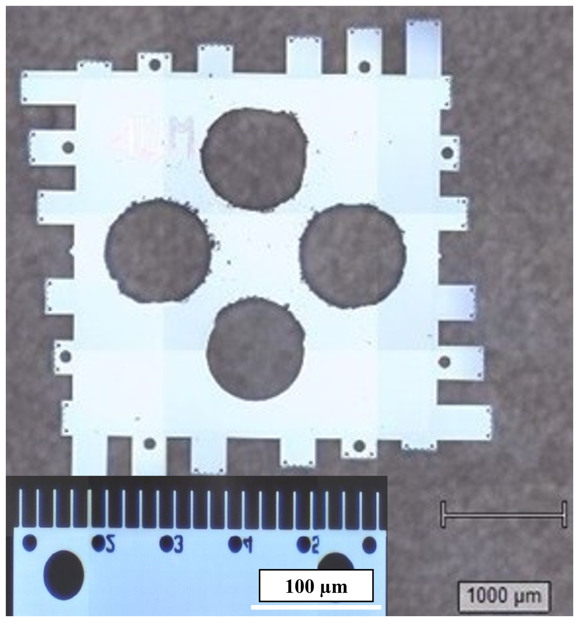
Figure 1Optical microscopy image of a CNT growth substrate. On each of the four chip sides, six forks can be seen. Inset: one fork structure with 21 trenches between SOI beams.
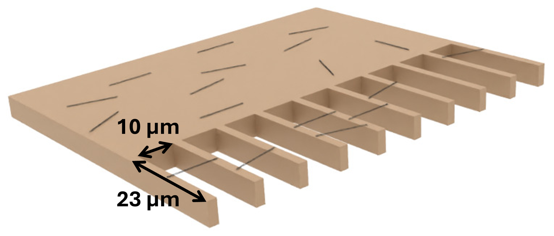
Figure 2Illustration of a portion of the CNT growth substrate. The CNTs are CVD-grown from a catalyst on the whole growth substrate, including on the comb structures. Some CNTs bridge the trenches to form suspended CNTs.
The SEM measurements were done using SU8200 equipment made by Hitachi. A working distance of 4.6 mm, an acceleration voltage of 1.0 kV, a beam current of 10.5 nA, and an image acquisition time of 20 s were used. CNTs were visually counted directly from the resulting images.
To determine the Raman yield, Raman spectroscopy measurements were conducted using the Renishaw inVia Qontor system, employing the StreamLine™ scanning method with an elliptical laser beam cross-section. The laser was focused on the sample using a microscope objective with 50× magnification and a numerical aperture (NA) of 0.75. This was done to visualize all bridging CNTs. Most measurements were done with a step distance between measurement lines of 1 µm or lower (the lines were oriented parallel to the longitudinal axes of the silicon beams). In our case, measurements took around 1 h per fork and wavelength. The data provided by these measurements were then used to create visual maps, made possible by Renishaw's software WiRE 5.6, as can be seen in Fig. 3. To create those maps, the Raman intensity of the measurements was filtered at G and D* band locations, seen in Fig. 4, around 1585 cm−1 for the G band and around 2665 cm−1 with a wavelength of 514 nm and 2695 cm−1 with a wavelength of 488 nm for the D* band. For those bands to be visible, the resonance condition for incoming or outgoing (scattered) light must be fulfilled (Dresselhaus et al., 2005). This is only the case when the laser light energy corresponds to the optically allowed transition between the van Hove singularities of the electronic structure of these one-dimensional tubes (Dresselhaus et al., 2005). If the resonance condition was met, with a maximum deviation of about ±0.1 eV (Saito et al., 2011), and the resulting signal-to-noise ratio was above 1.5, the CNTs would appear in the map created through the WiRE software. In that case, the suspended CNTs were manually counted from those maps.
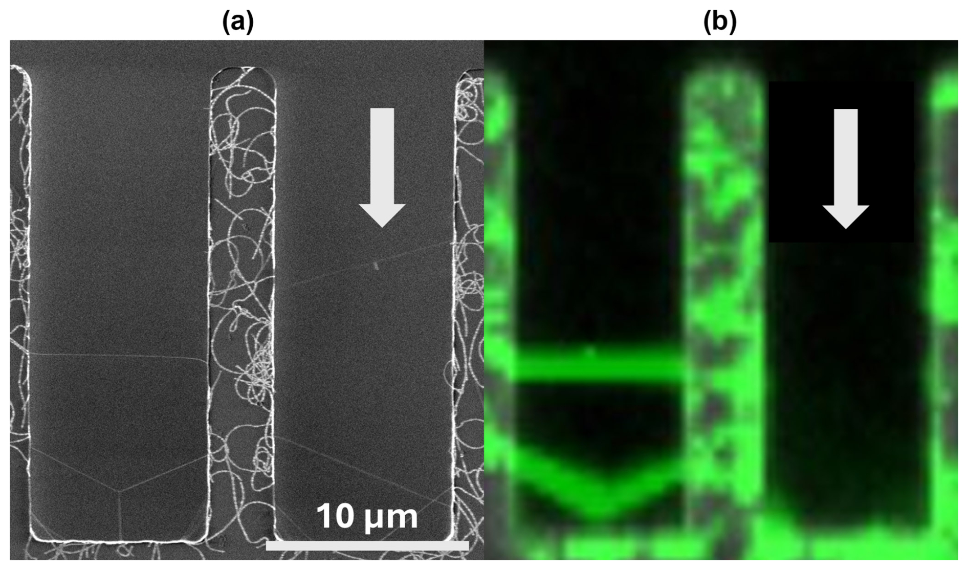
Figure 3SEM image (a) and Raman measurement map (b) showing the same two trenches of growth substrate's fork. CNTs detected by Raman spectroscopy are highlighted in green. The white arrows indicate a CNT that is visible in the SEM image but not detectable using 514 nm Raman spectroscopy.
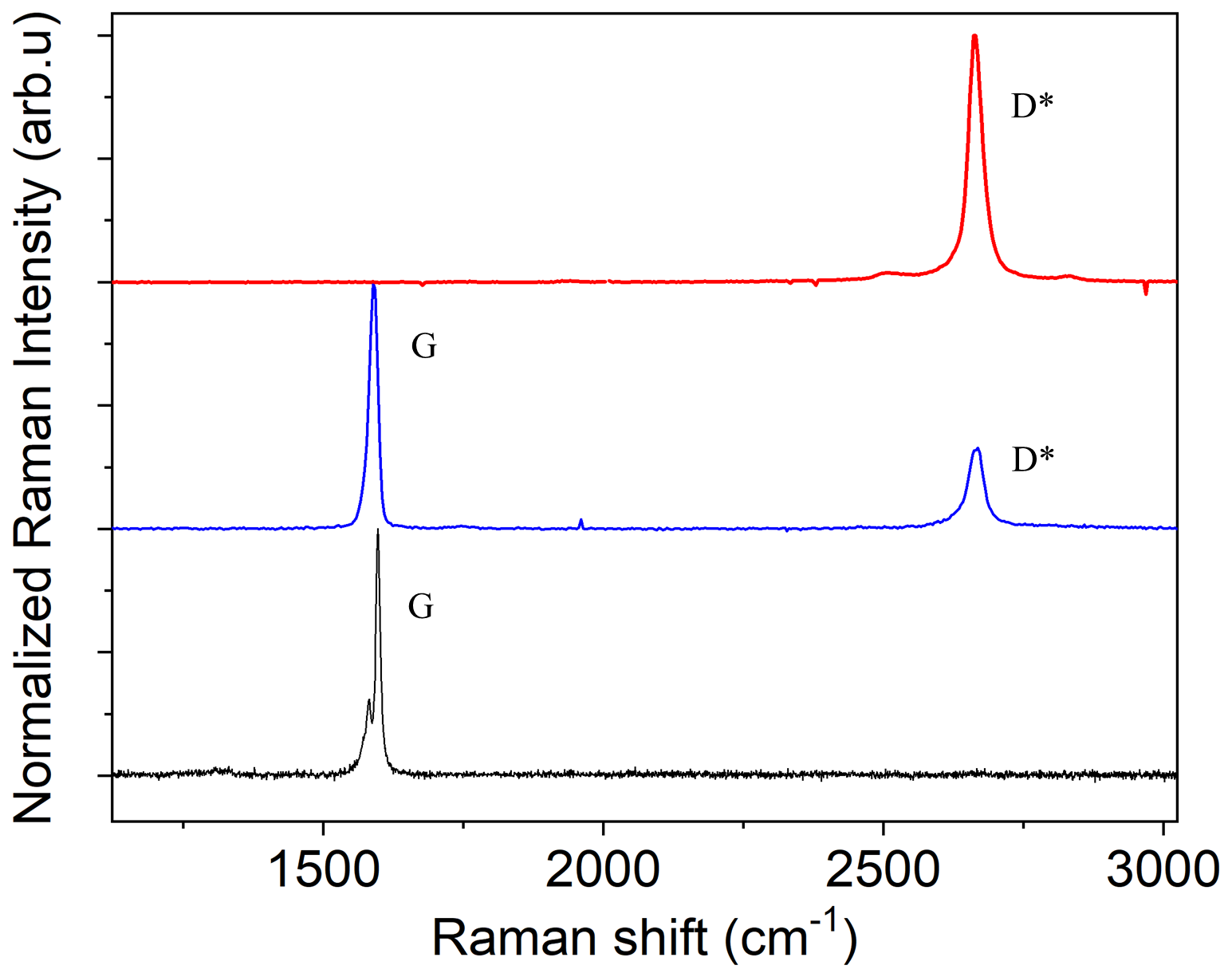
Figure 4Raman spectra of three CNTs. The bands G (left, at around 1585 cm−1) and D* (right, at around 2665 cm−1) are differently visible for each CNT. The spectra are vertically shifted and normalized to the dominant peak. By filtering the Raman data around the G and D* peaks, maps of the Raman visibility of the CNTs can be made.
3.1 CNT visibility using two laser wavelengths
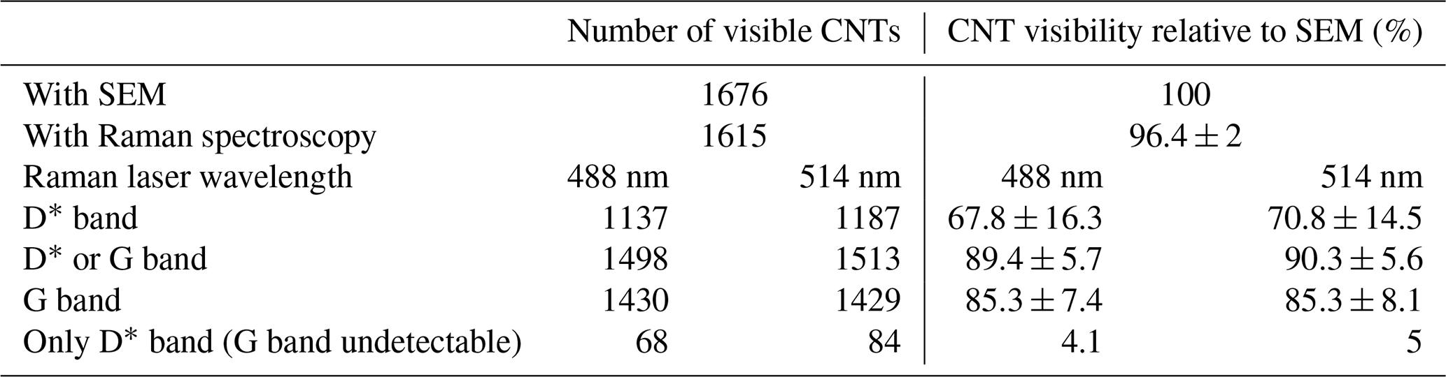
Of 1676 SEM-visible CNTs, 1615, or 96.4 %, were visible in Raman spectroscopy when evaluating both detection yields obtained by the 488 and 514 nm wavelengths, as well as with both G and D* bands. Considering only the G band offers a CNT visibility of 85.3 % for both the 488 and 514 nm wavelengths. For maps only filtered by the D* band, 67.8 % of CNTs were visible using the 488 nm wavelength, and 70.8 % were visible using the 514 nm wavelength. Combining the D* and G band maps, a total of 89.4 % and 90.3 % of CNTs were visible for the 488 and 514 nm wavelengths, respectively. Some of the CNTs – 4.1 % and 5 % for the wavelengths of 488 and 514 nm, respectively – showed only the peak of the D* band, while the intensity of their G band was comparable to the noise level. These results are summarized in Table 1.
Table 1CNT visibility for different laser wavelengths (488 and 514 nm) and CNT-specific Raman spectroscopy bands (the G band at around 1585 cm−1 and the D* band at around 2665 cm−1). Uncertainty is estimated based on the detection yield fluctuations between the CNT growth chips as 13σyield (see the Supplement for the calculation of the sample standard deviation σyield).
3.2 Theoretically expected CNT visibility using two laser wavelengths
Experimental values were compared to simulated values derived from the calculated SWCNT's electronic structures represented by the Kataura plot (Liu et al., 2012). The simulation assesses the energy provided by the laser wavelengths and compares it to the energy required to fulfill the resonance condition (±0.1 eV), making CNTs detectable via Raman spectroscopy. Since resonance depends on the CNT chiral indices, the diameter distribution influences the calculated visibility. The result from this simulation for the CNT diameter distribution of 1.9 ± 0.27 nm, as found by Durrer et al. (2009), is presented in Table 2 and is ∼ 15.3 % lower than the experimentally measured yield.
Table 2Theoretical CNT detectability with Raman spectroscopy for the expected diameter distribution of 1.9 ± 0.27 nm and for that of 2.735 ± 0.27 nm using the 488 and the 514 nm laser wavelengths. The visibility is given for the CNT-specific Raman spectroscopy peaks: the G band at around 1585 cm−1 and the D* band at around 2665 cm−1. The table shows that the CNT visibility depends on the CNT diameter and the excitation laser wavelength.
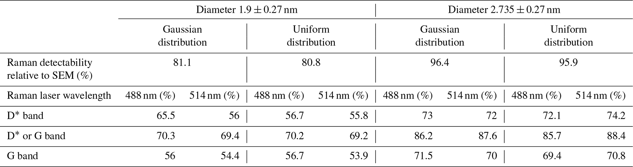
The difference between the theoretically expected Raman yield for CNTs with the diameter distribution mentioned by Durrer et al. (2009) and that of this work can be explained by the possibility that the CNT diameter distributions are different to what is assumed. When simulating the detection yield for larger diameters, as can be seen in Table 2 for a diameter distribution of 2.735 nm ± 0.27 nm, the theoretical detection yield could be increased to match the experimentally measured detection yield of 96.4 % (here, for a Gaussian diameter distribution). This raises the possibility that the suspended CNTs investigated in this work have larger diameters than those studied by Durrer et al. (2009). However, measurements of the RBM band for SWCNTs with such a diameter distribution are partly outside the measurable range of the Raman system used.
Another explanation for the high Raman yield may be the counting methodology, where unresolved CNT bundles and multi-walled CNTs were counted as single entities in both SEM and Raman maps unless multiple radial breathing modes were observed. Such cases could account for the observed difference, particularly in high-density samples, where bundling probability increases. Approximately 700 of the 1676 counted CNTs originated from samples with such high-density trench-bridging CNTs (more than 15 suspended CNTs per fork). In our CNT samples, some CNTs appear as Y-shaped structures, as can be seen in the SEM image (bottom left) in Fig. 3. These kinds of CNTs (that are likely to be bundles of two or more CNTs) were counted as one CNT in SEM. However, they are likely to appear with Raman spectroscopy.
The CNT visibility with the D* band for a diameter distribution of 2.735 ± 0.27 nm was theoretically expected to be higher than our study shows, as can be seen in Tables 1 and 2. This deviation might be explained by the fact that the Raman signal for the D* band is usually much weaker compared to the G band for the case when resonance conditions for excitation laser wavelength are fulfilled, and, therefore, it could be more easily covered by noise.
When comparing chips with low and high densities of suspended CNTs across all samples, those with a lower CNT density, representing 37 % of the total measured CNT amount, had an average detection yield of 95.2 %, whereas high-density chips achieved an average yield of 97.0 %. This suggests that CNT density plays a role in influencing the Raman spectroscopy detection yield for the reasons discussed above.
To decrease the risk of unintended integration of more than one CNT into a sensor device, a third excitation laser wavelength can be used for additional Raman mapping to further increase the detection probability. For example, considering the application of a 785 nm excitation laser wavelength, in addition to the two above-mentioned laser wavelengths, to the set of CNTs with a diameter distribution of 1.9 ± 0.27 nm (or 2.735 ± 0.27 nm) will increase the theoretical probability of detection from around 0.81 (0.96) to 0.95 (0.97). To test this option, a separate and smaller subset of 205 CNTs was also measured using a third wavelength of 785 nm. The results from this experiment suggested an increase in the total Raman detection yield of up to 2.5 %. Although the subset was too small to draw definitive conclusions, it is evident that Raman spectroscopy detection yield benefits from incorporating an additional, distinct wavelength. While some individual laser wavelengths offer lower yields than the 488 or 514 nm wavelengths, as shown for different diameter distributions in Fig. 5, they could detect CNTs that are invisible to those other wavelengths, thereby increasing the overall Raman detection yield. As can be seen in Fig. 5, resulting from Kataura plot simulations, the usefulness of laser wavelengths in detecting CNTs varies with the diameter distribution.
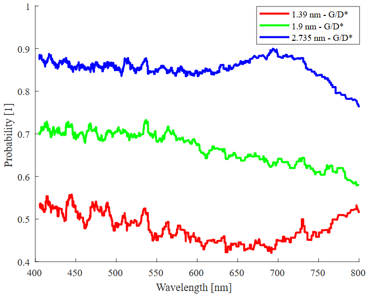
Figure 5Raman spectroscopy detection yield across various laser wavelengths considering both G and D* spectral bands. Detection yields were simulated for three CNT diameter distributions, with average diameters of (from top to bottom in the figure) 2.735, 1.9, and 1.39 nm. Each distribution follows a Gaussian profile, with a standard deviation of ±0.27 nm. The x axis represents the excitation laser wavelength, while the y axis indicates the probability of CNT detectability at each wavelength.
By comparing the detection yield of two laser wavelengths (488 and 514 nm) and by comparing these results to SEM imaging, we quantified CNT visibility using both the G and D* Raman bands. The overall Raman detection yield reached 96.4 %, significantly surpassing the individual yields from each wavelength. By adding a third wavelength, here 785 nm, the total yield could be improved further.
The findings highlight the usefulness of Raman spectroscopy as a non-destructive visualization method, particularly for simultaneously localizing CNTs and providing additional information on their properties (Zhang et al., 2022).
An interesting prospect for future work could involve utilizing the measured Raman detection yield to estimate the average CNT diameter, including cases where RBM bands are not detectable. By considering the laser wavelengths and the Raman spectroscopy detection yields, such estimations may be achievable. For example, detection yields of 95.2 % and 97 % could correspond to CNT populations with Gaussian diameter distributions of approximately 2.64 ± 0.27 and 2.79 ± 0.27 nm, respectively. This approach needs further research but could provide a method for characterizing the diameters of CNT populations with limited spectroscopic signatures.
Ultimately, multi-wavelength Raman spectroscopy proves to be a valuable tool in the optimization of CNT integration for sensor applications, particularly for the optimization of carbon-nanotube field-effect transistor (CNFET) gas sensor devices, where the limitation of one individual CNT can benefit the sensor power consumption, sensitivity, and limit of detection and can offer a better understanding of the response of different CNTs to different gases.
All of the measurement data are not publicly available but can be made available upon reasonable request to the corresponding author.
The supplement related to this article is available online at https://doi.org/10.5194/jsss-14-67-2025-supplement.
MH and IK designed the SEM and Raman spectroscopy experiments and supervised the data collection. NM carried out the SEM imaging, and NM and MH carried out the Raman spectroscopy measurements. CIR developed the script to calculate theoretically expected Raman spectroscopy detection yields. NM prepared the paper. All the authors have read and revised the paper. CH provided intellectual inputs regarding the research study and reviewed and revised the paper for critical content.
The contact author has declared that none of the authors has any competing interests.
Publisher's note: Copernicus Publications remains neutral with regard to jurisdictional claims made in the text, published maps, institutional affiliations, or any other geographical representation in this paper. While Copernicus Publications makes every effort to include appropriate place names, the final responsibility lies with the authors.
This article is part of the special issue “Eurosensors 2024”. It is a result of the EUROSENSORS XXXVI, Debrecen, Hungary, 1–4 September 2024.
Our thanks go out to Ricardo Stirnimann for his help with the Raman spectroscopy, to Lukas Schürz for the sample preparation, and to the Micro- and Nanosystems group (MNS) of ETH Zürich, as well as the Binning and Rohrer Nanotechnology Centre (BRNC), for making it possible to conduct this study. ChatGPT-4o was used to improve the grammar and spelling of the initial drafts of this article; no content was generated. After using this tool, the authors reviewed and edited the content as needed and take full responsibility for the content of the publication.
This paper was edited by Michele Penza and reviewed by two anonymous referees.
Cialla-May, D., Schmitt, M., and Popp, J.: Theoretical principles of Raman spectroscopy, Phys. Sci. Rev., 4, 6, https://doi.org/10.1515/psr-2017-0040, 2019.
Chikkadi, K., Muoth, M., Roman, C., Haluska, M., and Hierold, C.: Advances in NO2 sensing with individual single-walled carbon nanotube transistors, Beilstein J. Nanotech., 5, 2179–2191, https://doi.org/10.3762/bjnano.5.227, 2014.
Cubaynes, T., Contamin, L. C., Dartiailh, M. C., Desjardins, M. M., Cottet, A., Delbecq, M. R., and Kontos, T.: Nanoassembly technique of carbon nanotubes for hybrid circuit-QED, Appl. Phys. Lett., 117, 114001, https://doi.org/10.1063/5.0021838, 2020.
Durrer, L., Greenwald, J., Helbling, T., Muoth, M., Riek, R., and Hierold, C.: Narrowing SWNT diameter distribution using size-separated ferritin-based Fe catalysts, Nanotechnology, 20, 355601, https://doi.org/10.1088/0957-4484/20/35/355601, 2009.
Dresselhaus, M. S., Dresselhaus, G., Jorio, A., Souza Filho, A. G., and Saito, R.: Raman spectroscopy on isolated single wall carbon nanotubes, Carbon, 40, 2043–2061, https://doi.org/10.1016/S0008-6223(02)00066-0, 2002.
Dresselhaus, M. S., Dresselhaus, G., Jorio, A., Souza Filho, A. G., and Saito, R.: Raman spectroscopy of carbon nanotubes, Phys. Rep., 409, 47–99, https://doi.org/10.1016/j.physrep.2004.10.006, 2005.
Jung, S., Hauert, R., Haluska, M., Roman, C., and Hierold, C.: Understanding and improving carbon nanotube-electrode contact in bottom-contacted nanotube gas sensors, Sens. Actuators B Chem., 331, 129406, https://doi.org/10.1016/j.snb.2020.129406, 2021.
Jung, S., Roman, C., and Hierold, C.: Fast Nitrogen Dioxide Sensing with Ultralow-Power Nanotube Gas Sensors, Adv. Sensor Res., 3, 2300081, https://doi.org/10.1002/adsr.202300081, 2024.
Kong, J., Franklin, N. R., Zhou, C., Chapline, M. G., Peng, S., Cho, K., and Dai, H.: Nanotube molecular wires as chemical sensors, Science, 287, 622–625, https://doi.org/10.1126/science.287.5453.622, 2000.
Li, W., Hennrich, F., Flavel, B. S., Dehm, S., Kappes, M., and Krupke, R.: Principles of carbon nanotube dielectrophoresis, Nano Res., 14, 2188–2206, https://doi.org/10.1007/s12274-020-3183-0, 2021.
Liu, K., Deslippe, J., Xiao, F., Capaz, R. B., Hong, X., Aloni, S., Zettl, A., Wang, W., Bai, X., and Louie, S. G.: An atlas of carbon nanotube optical transitions, Nat. Nanotechnol., 7, 325–329, https://doi.org/10.1038/nnano.2012.52, 2012.
Muoth, M. and Hierold, C.: Transfer of carbon nanotubes onto microactuators for hysteresis-free transistors at low thermal budget, IEEE 25th Int. Conf. Micro Electro Mech. Syst. (MEMS), Paris, France, 2012, 1352–1355, https://doi.org/10.1109/MEMSYS.2012.6170417, 2012.
Popov, N.: Carbon nanotubes: properties and application, Mater. Sci. Eng. R Rep., 43, 61–102, https://doi.org/10.1016/j.mser.2003.10.001, 2004.
Saito, R., Hofmann, M., Dresselhaus, G., Jorio, A., and Dresselhaus, M. S.: Raman spectroscopy of graphene and carbon nanotubes, Adv. Phys., 60, 413–550, https://doi.org/10.1080/00018732.2011.582251, 2011.
Schroeder, V., Savagatrup, S., He, M., Lin, S., and Swager, T. M.: Carbon Nanotube Chemical Sensors, Chem. Rev., 119, 599–663, https://doi.org/10.1021/acs.chemrev.8b00340, 2018.
Tans, S. J., Devoret, M. H., Dai, H., Thess, A., Smalley, R. E., Geerligs, L. J., and Dekker, C.: Individual single-wall carbon nanotubes as quantum wires, Nature, 386, 474–477, https://doi.org/10.1038/386474a0, 1997.
Vandenabeele, P.: Practical Raman Spectroscopy: An Introduction, John Wiley & Sons, Ltd, https://doi.org/10.1002/9781119961284, 2013.
Zhang, J, Perrin, M. L, Barba, L., Overbeck, J., Jung, S., Grassy, B., Agal, A., Muff, R., Brönnimann, R., Haluska, M., Roman, C., Hierold, C., Jaggi, M., and Calame, M.: High-speed identification of suspended nanotubes using Raman spectroscopy and deep learning, Microsyst. Nanoeng., 8, 19, https://doi.org/10.1038/s41378-022-00350-w, 2022.