the Creative Commons Attribution 4.0 License.
the Creative Commons Attribution 4.0 License.
 | 14 Jan 2022
Numerical analysis of an infrared gas sensor utilizing an indium-tin-oxide-based plasmonic slot waveguide
Bernhard Jakoby
Gerald Pühringer
Andreas Tortschanoff
Gerald Stocker
Jasmin Spettel
Thomas Grille
Reyhaneh Jannesari
Plasmonic waveguides have attracted much attention owing to the associated high field intensity at the metal–dielectric interface and their ability to confine the modes at the nanometer scale. At the same time, they suffer from relatively high propagation loss, which is due to the presence of metal. Several alternative materials have been introduced to replace noble metals, such as transparent conductive oxides (TCOs). A particularly popular TCO is indium tin oxide (ITO), which is compatible with standard microelectromechanical systems (MEMS) technology. In this work, the feasibility of ITO as an alternative plasmonic material is investigated for infrared absorption sensing applications: we numerically design and optimize an ITO-based plasmonic slot waveguide for a wavelength of 4.26 µm, which is the absorption line of CO2. Our optimization is based on a figure of merit (FOM), which is defined as the confinement factor divided by the imaginary part of the effective mode index (i.e., the intrinsic damping of the mode). The obtained optimal FOM is 3.2, which corresponds to 9 µm and 49 % for the propagation length (characterizing the intrinsic damping) and the confinement factor, respectively.
- Article
(428 KB) - Full-text XML
- BibTeX
- EndNote


In recent years, plasmonic effects and devices have commanded increased attention, as they enable sub-wavelength photonics applications. The existence of surface plasmon polaritons (SPPs), which are essentially guided electromagnetic waves propagating along a metal–dielectric interface with strong near-field confinement, allows for efficient light–matter interactions (Prämassing et al., 2020; Gaur et al., 2021). For the guided mode, the maximum intensity occurs at the metal–dielectric interface where the field amplitudes decay exponentially in the direction perpendicular to the interface (Dionne et al., 2006). This so-called evanescent field represents the bound, non-radiative nature of SPPs (Barnes et al., 2003). A plasmonic device that has attracted particular attention is the plasmonic waveguide. A specific merit of SPP-based waveguides is that they can break the diffraction limit related to the dielectric waveguides, leading to strong field confinement (Sun et al., 2014). Among the plasmonic waveguides, plasmonic slot waveguides are particularly attractive due to the provided lateral confinement and the capability of guiding the mode in low-index materials, which can be an asset in the fabrication of miniaturized optical circuits. Therefore, compared with dielectric waveguides, they allow compact integration and short coupling lengths (Osowiecki et al., 2014). Furthermore, as plasmonic slot waveguides allow for a high-energy fraction in low-index material, they promise high sensitivity with respect to absorption in a gaseous sensing medium, acting as a low-index medium in such a sensor.
Traditionally, noble metals have been widely used as plasmonic materials due to their chemical stability, large plasma frequency and high electrical conductivity (Paulraj et al., 2020). However, they typically suffer from high intrinsic losses and high costs, hampering practical applications (Chen et al., 2017). As alternatives to noble metals, transparent conductive oxides (TCOs) can be considered. They not only show a low loss in the infrared range but their compatibility with standard microfabrication also makes them particularly appealing for the simple integration of plasmonic devices (Wang et al., 2017). Another feature of TCOs is that their optical and electrical properties can be tuned by changing the doping concentration. In addition, TCOs are often fabricated using thin-film technology and are utilized in optoelectronic applications, such as electrode materials in biosensors and other sensors (Sohn et al., 2011). Among TCOs, indium tin oxide (ITO) has attracted particular attention from many scientists and researchers due to its surface smoothness, mechanical stability, robustness in moist air and simple fabrication (Dao et al., 2019). Therefore, it has been used in many studies related to optical meta-surfaces (Shrestha et al., 2018), localized plasmonic nanoparticles (Xi et al., 2018) and active tuneable plasmonic devices (Liu et al., 2018). Moreover, ITO is an appropriate material for sensing applications owing to unique features such as high electrical conductivity, substrate adhesion, and electrochemical and physical stability (Aydin et al., 2017). However, as ITO is a non-stoichiometric compound, its optical properties crucially depend on the fabrication processes such as growth and deposition procedures as well as on annealing conditions (West et al., 2010). It has already been shown that sputtering power and annealing processes can affect the optical properties of ITO in the mid-infrared spectrum (Wang et al., 2017). ITO thin films can be produced using technologies such as magnetron sputtering, electron beam evaporation and chemical vapor deposition. Among these methods, magnetron sputtering is widely used due to the better film quality, faster deposition rate and the associated repeatability (Zhang et al., 2020).
Although ITO has been introduced as a desirable plasmonic material to replace noble metals, to the author's knowledge, it has neither been studied in detail theoretically nor experimentally for application in waveguiding systems to date. We consider ITO for waveguiding systems because it shows a high carrier density which makes it a suitable alternative plasmonic material in the near- and mid-infrared region. In this paper, a plasmonic slot waveguide based on ITO has been designed and numerically analyzed for sensing applications. Our sensor platform is designed for a wavelength of 4.26 µm, which corresponds to the absorption peak of CO2, and serves as an example of the application of infrared absorption sensing in gases. We used an ITO-based slot waveguide on top of 2 µm silica as a substrate, as illustrated in Fig. 1. In practice, this substrate can be an oxidized silicon wafer. In the simulation, the region to be occupied by the sensing medium in the final application is associated with a refractive index of 1, as we are studying the properties of the guided mode. The modal properties of the proposed structure have been investigated using the finite element method (FEM) implemented by the COMSOL Multiphysics software (COMSOL, 2022). The refractive index of SiO2 and ITO at 4.26 µm is and (Wang et al., 2017), respectively.

Figure 1Cross-sectional view of an ITO-based plasmonic slot waveguide. The blue region, which consists of the slot region and upper cladding, is considered as the sensing medium.
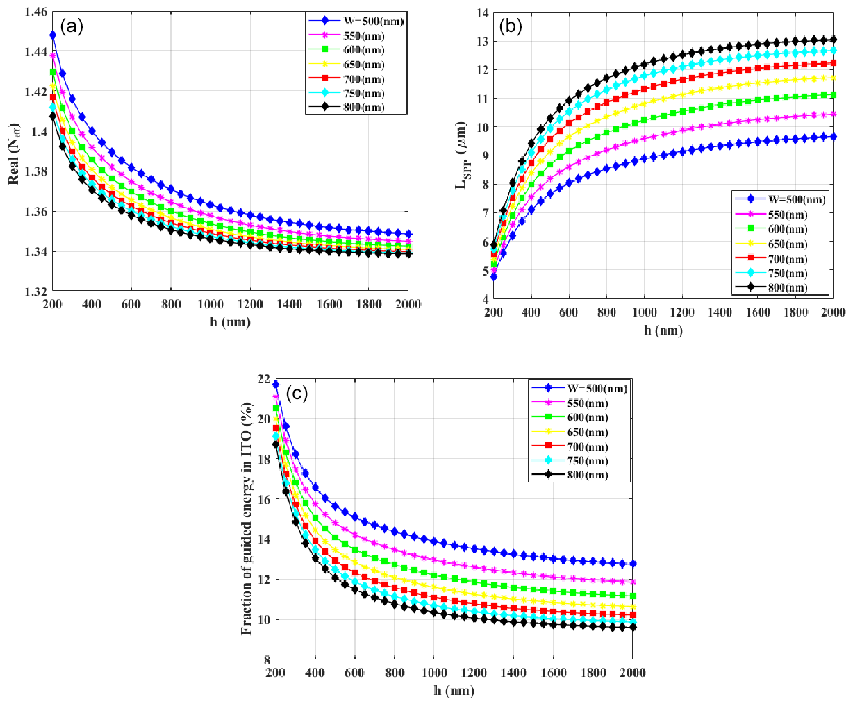
Figure 2(a) The real part of the effective mode index (Neff), (b) the propagation length (LSPP) and (c) the fraction of guided electromagnetic energy in ITO versus slot height (h) for different slot widths (w).
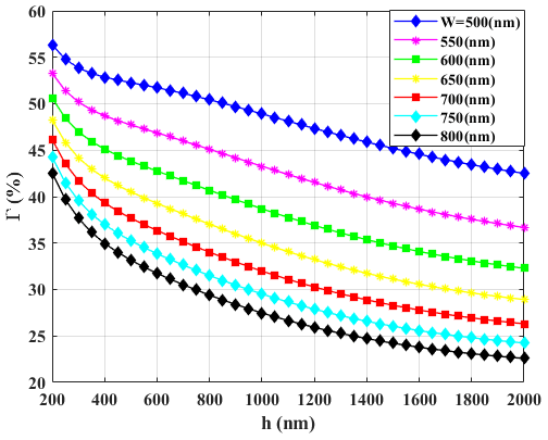
Figure 3The confinement factor (Γ) as a function of slot height (h) for different slot widths (w).
The preliminary results of this study were presented at the Sensors and Measurement Science International (SMSI) conference in 2021 (Saeidi et al., 2021a). In the conference paper, our sensor platform had been optimized based on the figures of merit (FOM) as a product of the evanescent field ratio and propagation length. In the current work, to consider the effect of group velocity, the confinement factor including both the evanescent field ratio and group velocity has been evaluated. Therefore, our sensor platform is optimized based on a FOM, which is defined as the confinement factor divided by the imaginary part of the effective mode index. Our aim is to optimize the waveguide geometries to reach the optimal propagation length and confinement factor simultaneously.
2.1 Propagation length
One of the crucial parameters for sensing applications is propagation length (LSPP). The LSPP of an SPP mode is defined as a distance over which the intensity of the SPP mode reduces to of its original value. The calculation of LSPP has been discussed in Spettel et al. (2021) and Stocker et al. (2021). In any kind of plasmonic waveguide, the presence of metal or metal-like material causes the plasmonic waveguide to be lossy. We note that, in the present work, potential additional losses due to the surface roughness are not considered.
The real part of the effective mode index (, where KSPP and K0 are the wave vectors of the SPP mode and free-space light, respectively) of the fundamental SPP mode of a plasmonic slot waveguide as a function of slot thickness (h) is depicted in Fig. 2a. Increasing h results in decreasing Neff. Moreover, for a given h, Neff decreases with increasing slot width (w), which is due to less field confinement in the slot region (Heydari et al., 2020). Furthermore, the LSPP for a given h, shown in Fig. 2b, increases with increasing w because the fraction of guided electromagnetic energy in the ITO rails decreases (see Fig. 2c), which reduces the intrinsic loss associated with the ITO. Similarly, increasing h leads to an increase in LSPP for the same reason.
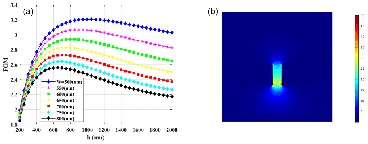
Figure 4(a) The figures of merit (FOM) as a function of slot height (h) for different slot widths (w). (b) The x component of the electric field distribution (Ex) of the SPP mode for optimum values of the structure.
2.2 Confinement factor
Light absorption in a waveguide that is placed in a sensing medium can be described using a generalized Beer–Lambert law (Vlk et al., 2021):
where I and I0 indicate the measured intensity and the initial intensity at a particular CO2 concentration c, respectively; Γ is the confinement factor; α is the absorption coefficient; and L is the interaction path length.
Based on this law, the confinement factor (Γ) plays a major role in the sensitivity of the sensor. The Γ, which includes both the evanescent field ratio (EFR) and group velocity (Vg), can describe the efficiency of light–matter interaction. The EFR describes the amount of electromagnetic energy present in the evanescent field which interacts with the analyte (e.g., gas in our case). When the sensor platform is placed in a gaseous medium to be sensed, which essentially forms the cladding, the evanescent field interacts with the gas via absorption along the waveguide. A high EFR indicates that the sensor interacts more efficiently with the analyte, which eventually improves the sensitivity of the device. The EFR can be calculated as follows:
where indicates the electric field vector, and ε is the permittivity of each material. The integrals extend across the cross section of the waveguide (orthogonally with respect to the propagation direction), which is assumed to be in the xy plane here. The integral in the numerator extends across the area filled by the analyte, whereas the integral in the denominator covers the entire cross section. The confinement factor (Γ) is defined as
where ng and nc are the group index () and refractive index of the cladding, respectively. The group velocity Vg corresponds to the speed of energy that flows through the cross section of the waveguide (Robinson et al., 2008). The mixture of both field delocalization and dispersion, which are characterized by EFR and Vg, respectively, can cause Γ to exceed unity, which means that the absorption per unit length in the propagation direction is larger than that achieved by a free-space beam. The confinement factor Γ of the fundamental mode of the plasmonic slot waveguide as a function of h for different w is given in Fig. 3. Increasing h leads to a reduction in Γ. Moreover, for a given h, increasing w results in less field being confined in the gap region and, correspondingly, more field penetrating the silica substrate, which results in a decrease in Γ.
There is a trade-off between and Γ. To quantize their trade-off, we define a dimensionless FOM as follows:
This FOM acts as an indicator of the waveguide sensitivity. The FOM of the ITO-based plasmonic slot waveguide as a function of h is illustrated in Fig. 4a. The optimal FOM is 3.2, which is associated with w=500 nm and h=1000 nm. The obtained FOM corresponds to roughly 49 % and 9 µm for Γ and LSPP, respectively. In comparison to the plasmonic slot waveguides that are reported in Saeidi et al. (2021b), the proposed structure shows a lower FOM which is mainly due to its low propagation length. However, the Γ provided by the structure is higher than that reported in Saeidi et al. (2021b). Further, compared with the dielectric waveguide structures that are designed for the same purpose (Ranacher et al., 2018a, b), the present design features a lower FOM, but it again represents a higher Γ. We note that the optimization of the ITO-based plasmonic slot waveguide presented in this work is performed for a wavelength of 4.26 µm, which is the absorption line of CO2. To consider the performance of the proposed waveguide for other gases, different refractive indices have to be used in the model and yield different FOMs, although the general approach remains the same.
In plasmonic slot waveguides, the x component of the electric field distribution (Ex) is a major component that indicates lateral confinement. Figure 4b shows the Ex of the SPP mode for the optimized parameters of the structure, clearly illustrating that the mode is confined in the slot region, although a part of it penetrates the silica substrate.
We investigated the feasibility of ITO as an alternative plasmonic material to replace noble metals for sensing applications in the mid-infrared region. Considering a specific example, an ITO-based plasmonic slot waveguide was designed and numerically analyzed for a wavelength of 4.26 µm, which is the absorption band of CO2. The plasmonic slot waveguide was optimized based on a figure of merit (FOM) composed of the product of the propagation length and the confinement factor, which are two crucial quantities in sensing applications. The achieved optimal FOM is 3.2, which is associated with 9 µm and 49 % for the propagation length and confinement factor, respectively. As the optical properties of ITO are highly dependent on the fabrication process such as growth and deposition process and also on annealing conditions, based on the adopted fabrication methods, the optical properties of ITO, such as the complex refractive index, can vary. Thus, the obtained FOM might change if another refractive index associated with another fabrication method is used. Nevertheless, the optimization approach introduced in this work can always be used to find the best geometrical parameters of any plasmonic slot waveguide.
As the proposed structure shows low propagation lengths, we finally have to conclude that ITO appears not to be an appropriate candidate for plasmonic waveguiding systems. However, based on the achieved high confinement factor, it could be an attractive material for applications in which a cavity or resonator would be used.
Research data are available upon request from the authors.
PS, AT, RJ and BJ conceptualized the study. PS, RJ and GP developed the methodology. PS was responsible for the software. PS and RJ carried out the validation process. PS prepared and wrote the original draft of the paper, and PS, BJ, RJ, GP, AT, GS, JS and TG reviewed and edited the paper. PS was responsible for the visualizations. BJ and RJ supervised the study. All authors have read and agreed upon the published version of the paper.
At least one of the (co-)authors is a member of the editorial board of Journal of Sensors and Sensor Systems.
Publisher’s note: Copernicus Publications remains neutral with regard to jurisdictional claims in published maps and institutional affiliations.
This article is part of the special issue “Sensors and Measurement Science International SMSI 2021”. It is a result of the Sensor and Measurement Science International, 3–6 May 2021.
This work has been funded by the COMET-K2 “Center for Symbiotic Mechatronics” of the Linz Center of Mechatronics (LCM) within Austrian Smart Systems Integration Research Center (ASSIC) funded by the Austrian federal government and the federal state of Upper Austria and by the PICASSO project funded by the BMVIT in the framework of the “Produktion der Zukunft” program (project no. 871417).
This paper was edited by Daniel Platz and reviewed by two anonymous referees.
Aydın, E. B. and Sezgintürk, M. K.: Indium tin oxide (ITO): a promising material in biosensing technology, TrAC-Trend Anal. Chem., 97, 309–315, https://doi.org/10.1016/j.trac.2017.09.021, 2017.
Barnes, W. L., Dereux, A., and Ebbesen, T. W.: Surface plasmon subwavelength optics, Nature, 424, 824–830, https://doi.org/10.1038/nature01937, 2003.
Chen, K., Guo, P., Dao, T. D., Li, S. Q., Ishii, S., Nagao, T., and Chang, R. P.: Protein-Functionalized Indium-Tin Oxide Nanoantenna Arrays for Selective Infrared Biosensing, Adv. Opt. Mat., 5, 1700091, https://doi.org/10.1002/adom.201700091, 2017.
COMSOL: Multiphysics® v. 5.6., available at: https://www.comsol.com/ (last access: 11 January 2022), COMSOL AB, Stockholm, Sweden, 2022.
Dao, T. D., Doan, A. T., Ngo, D. H., Chen, K., Ishii, S., Tamanai, A., and Nagao, T.: Selective thermal emitters with infrared plasmonic indium tin oxide working in the atmosphere, Opt. Mater. Express, 9, 2534–2544, https://doi.org/10.1364/OME.9.002534, 2019.
Dionne, J. A., Sweatlock, L. A., Atwater, H. A., and Polman, A.: Plasmon slot waveguides: Towards chip-scale propagation with subwavelength-scale localization, Phys. Rev. B, 73, 035407, https://doi.org/10.1103/PhysRevB.73.035407, 2006.
Gaur, R., Padhy, H. M., and Elayaperumal, M.: Surface plasmon assisted toxic chemical NO2 gas sensor by Au ZnO functional thin films, J. Sens. Sens. Syst., 10, 163–169, https://doi.org/10.5194/jsss-10-163-2021, 2021.
Heydari, M., Habibzadeh-Sharif, A., and Jabbarzadeh, F.: Design of a compact refractive-index sensor based on surface plasmon polariton slot waveguide, Photonic. Nanostruct., 38, 100755, https://doi.org/10.1016/j.photonics.2019.100755, 2020.
Liu, X., Kang, J. H., Yuan, H., Park, J., Cui, Y., Hwang, H. Y., and Brongersma, M. L.: Tuning of plasmons in transparent conductive oxides by carrier accumulation, Acs Photonics, 5, 1493–1498, https://doi.org/10.1021/acsphotonics.7b01517, 2018.
Osowiecki, G. D., Barakat, E., Naqavi, A., and Herzig, H. P.: Vertically coupled plasmonic slot waveguide cavity for localized biosensing applications, Opt. Express, 22, 20871–20880, https://doi.org/10.1364/OE.22.020871, 2014.
Paulraj, P., Umar, A., Rajendran, K., Manikandan, A., Kumar, R., Manikandan, E., and Baskoutas, S.: Solid-state synthesis of Ag-doped PANI nanocomposites for their end-use as an electrochemical sensor for hydrogen peroxide and dopamine, Electrochim. Acta, 363, 137158, https://doi.org/10.1016/j.electacta.2020.137158, 2020.
Prämassing, M., Liebtrau, M., Schill, H. J., Irsen, S., and Linden, S.: Interferometric near-field characterization of plasmonic slot waveguides in single-and poly-crystalline gold films, Opt. Express, 28, 12998–13007, https://doi.org/10.1364/OE.384629, 2020.
Ranacher, C., Consani, C., Tortschanoff, A., Jannesari, R., Bergmeister, M., Grille, T., and Jakoby, B: Mid-infrared absorption gas sensing using a silicon strip waveguide, Sensors Actuat. A-Phys., 277, 117–123, https://doi.org/10.1016/j.sna.2018.05.013, 2018a.
Ranacher, C., Consani, C., Vollert, N., Tortschanoff, A., Bergmeister, M., Grille, T., and Jakoby, B.: Characterization of evanescent field gas sensor structures based on silicon photonics, IEEE Photonics J., 10, 1–14, https://doi.org/10.1109/JPHOT.2018.2866628, 2018b.
Robinson, J. T., Preston, K., Painter, O., and Lipson, M.: First-principle derivation of gain in high-index-contrast waveguides, Opt. Express, 16, 16659–16669, https://doi.org/10.1364/OE.16.016659, 2008.
Saeidi, P., Jakoby, B., Pühringer, G., Tortschanoff, A., Stocker, G., Dubois, F., and Jannesari, R.: Designing Mid-Infrared Gold-Based Plasmonic Slot Waveguides for CO2-Sensing Applications, Sensors, 21, 2669, https://doi.org/10.3390/s21082669, 2021a.
Saeidi, P., Jakoby, B., Pühringer, G., Tortschanoff, A., Grille, T., and Jannesari, R.: Optimization of ITO-based plasmonic slot waveguide for CO2 mid-IR absorption sensors, https://doi.org/10.5162/SMSI2021/B9.3, 2021b.
Shrestha, S., Wang, Y., Overvig, A. C., Lu, M., Stein, A., Negro, L. D., and Yu, N.: Indium tin oxide broadband metasurface absorber, ACS Photonics, 5, 3526–3533, https://doi.org/10.1021/acsphotonics.8b00781, 2018.
Sohn, S. and Han, Y. S.: Transparent conductive oxide (TCO) films for organic light emissive devices (OLEDS), Organic Light Emitting Diode-Material, Process and Devices, 233-273, ISBN 978-953-307-273-9, 2011.
Spettel, J., Stocker, G., Dao, T. D., Jannesari, R., Tortschanoff, A., Saeidi, P., Pühringer, G., Dubois, F., Fleury, C., Consani, C., Grille, T., Aschauer, E., Moridi, M., and Jakoby, B.: Aluminium, gold-tin and titanium-tungsten alloys for mid-infrared plasmonic gratings, Opt. Mater. Express, 11, 1058–1069, https://doi.org/10.1364/OME.417877, 2021.
Stocker, G., Spettel, J., Dao, T. D., Tortschanoff, A., Jannesari, R., Pühringer, G., Saeidi, P., Dubois, F., Fleury, C., Consani, C., Grille, T., Aschauer, E., and Jakoby, B.: Ultra-Narrow SPP Generation from Ag Grating, Sensors, 21, 6993, https://doi.org/10.3390/s21216993, 2021.
Sun, X., Alam, M. Z., Mojahedi, M., and Aitchison, J. S.: Confinement and integration density of plasmonic waveguides, IEEE J. Sel. Top. Quant., 21, 268–275, https://doi.org/10.1109/JSTQE.2014.2377636, 2014.
Vlk, M., Datta, A., Alberti, S., Yallew, H. D., Mittal, V., Murugan, G. S., and Jágerská, J.: Extraordinary evanescent field confinement waveguide sensor for mid-infrared trace gas spectroscopy, Light: Science & Applications, 10, 1–7, https://doi.org/10.1038/s41377-021-00470-4, 2021.
Wang, Y., Overvig, A. C., Shrestha, S., Zhang, R., Wang, R., Yu, N., and Dal Negro, L.: Tunability of indium tin oxide materials for mid-infrared plasmonics applications, Opt. Mater. Express, 7, 2727–2739, https://doi.org/10.1364/OME.7.002727, 2017.
West, P. R., Ishii, S., Naik, G. V., Emani, N. K., Shalaev, V. M., and Boltasseva, A.: Searching for better plasmonic materials, Laser Photonics Rev., 4, 795–808, https://doi.org/10.1002/lpor.200900055, 2010.
Xi, M. and Reinhard, B. M.: Localized surface plasmon coupling between mid-IR-resonant ITO nanocrystals, J. Phys. Chem. C, 122, 5698–5704, https://doi.org/10.1021/acs.jpcc.8b01283, 2018.
Zhang, Y., Li, Q., Tian, Z., Hu, P., Qin, X., and Yun, F.: Gas-sensing properties of ITO materials with different morphologies prepared by sputtering, SN Applied Sciences, 2, 1–11, https://doi.org/10.1007/s42452-020-2050-7, 2020.