the Creative Commons Attribution 4.0 License.
the Creative Commons Attribution 4.0 License.
 | 24 Jul 2025
Silicon-based thermal conductivity detector for gas sensing and gas chromatography
Mathis Baret
Murielle Jurdit
Florence Ricoul
Jean-Baptiste Tissot
We present a novel thermal conductivity detector (TCD) for gas sensing and gas chromatography. Its original architecture is based on a suspended membrane on top of which a heating element made of titanium nitride and a separated sensing element made of amorphous silicon are deposited. These sensors are micro-fabricated from 200 mm silicon wafers and tested on a gas bench. When used as a standalone gas sensor, they reach a theoretical detection limit (3σ) of 13 ppm for carbon dioxide in the air and exhibit a signal-to-noise ratio 4 times higher than that of conventional platinum TCDs.
- Article
(2655 KB) - Full-text XML
- BibTeX
- EndNote


Thermal conductivity detectors (TCDs) are among the most widely used sensors in gas chromatography (GC) systems and are well appreciated for their universality and high dynamic range (Hinshaw, 2006). Recently, miniaturized TCDs (µTCDs) have been produced on silicon substrates using micro-electro-mechanical system (MEMS) micro-fabrication techniques (Kaanta et al., 2009; Sun et al., 2011; Legendre et al., 2017; Gardner et al., 2023). This level of integration greatly improves the sensitivity of this technology (Pecsar et al., 1973), allowing us to reach the sub parts per million (ppm) detection limit when coupled to a GC system (Regmi and Agah, 2018). Moreover, miniaturization reduces the power consumption of the detector (Berndt et al., 2020; Cho et al., 2022), opening up the way to portable air quality monitoring systems without necessarily having to couple the TCD to a GC column and preconcentrator. From that perspective, Bourlon et al. (2018) reported the use of a single µTCD chip to measure the CO2 concentration and relative humidity in the air simultaneously, with respective errors of 300 ppm and 2 %. However, TCDs are less sensitive than the flame ionization detectors (FIDs) or photoionization detectors (PIDs) also used in GC systems. Several approaches have been explored to increase the performances of TCDs, such as optimizing the TCD heating wire and chip design (Sun et al., 2020; Tan et al., 2020), protecting the sensing element from gas flow to reduce noise and flow influence (De Graaf et al., 2016), exploiting new detection schemes (Mahdavifar et al., 2015; Struk et al., 2018), and using new sensing materials with high sensitivity to temperature changes. Nevertheless, most of the material candidates with a high sensitivity to temperature also have a high electric resistivity and therefore cannot be used as self-heating temperature-sensitive elements where a low electric resistance value is needed. In this work, we propose a new type of TCD based on the use of two wires: one is used as a heating element to indirectly increase the temperature of a second wire used as the sensing probe and whose material has been chosen for its high sensitivity to temperature changes.
µTCDs are generally made of a suspended metallic wire heated by means of the Joule effect. The generated heat is dissipated into the surrounding gas depending on its thermal conductivity. Therefore, the TCD final temperature depends on the concentration and nature of the gas that surrounds it. This temperature is monitored by measuring the electrical resistance variation of the metallic wire. Indeed, the wire is often made of platinum or nickel, which have a very accurate and repeatable resistance-versus-temperature relationship. This relationship is, to a great extent, linear and is described by the temperature coefficient of resistance (TCR), noted as α. Therefore, the electrical resistance of the heated wire reflects its temperature, which, in turn, reflects the surrounding gas thermal conductivity.
A way to measure precisely the resistance variation is to use a Wheatstone bridge configuration (Sun et al., 2011) (Fig. 1). This consists of combining four suspended metallic wires or thermistors on the same silicon chip in order to have an accurate differential measurement of the resistance variations. Two of the thermistors are located in a reference channel in which the gas mixture flows before GC separation. The other two thermistors are located in an analysis channel where the different compounds flow after separation.
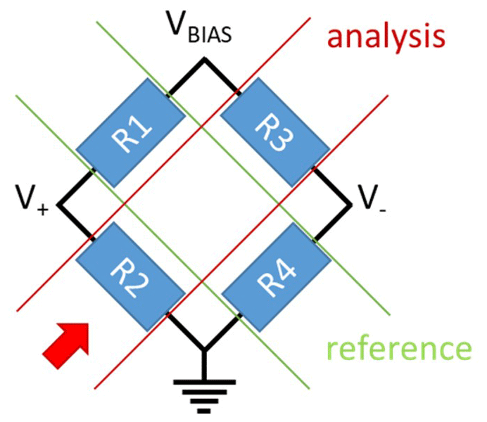
Assuming a resistive behaviour of the sensing elements and according to Ohm's law, the Wheatstone bridge signal can be expressed with Eq. (1):
For a given bias voltage, the signal reflects the sensing element's resistance variations that are, themselves, dependent on their temperature.
Several materials are known for their high TCRs, such as graphene (Peng et al., 2021) or zinc oxide (Zhou et al., 2014). However, in this work, boron-doped hydrogenated amorphous silicon (a-Si: H(B)) was chosen for its complementary metal–oxide–semiconductor (CMOS) compatibility and high sensitivity (Ketroussi et al., 2021). We have estimated the temperature coefficient of resistance (TCR) to be K−1 by means of a four-probe measurement of the sheet resistance as a function of temperature on a full wafer (Fig. 2).
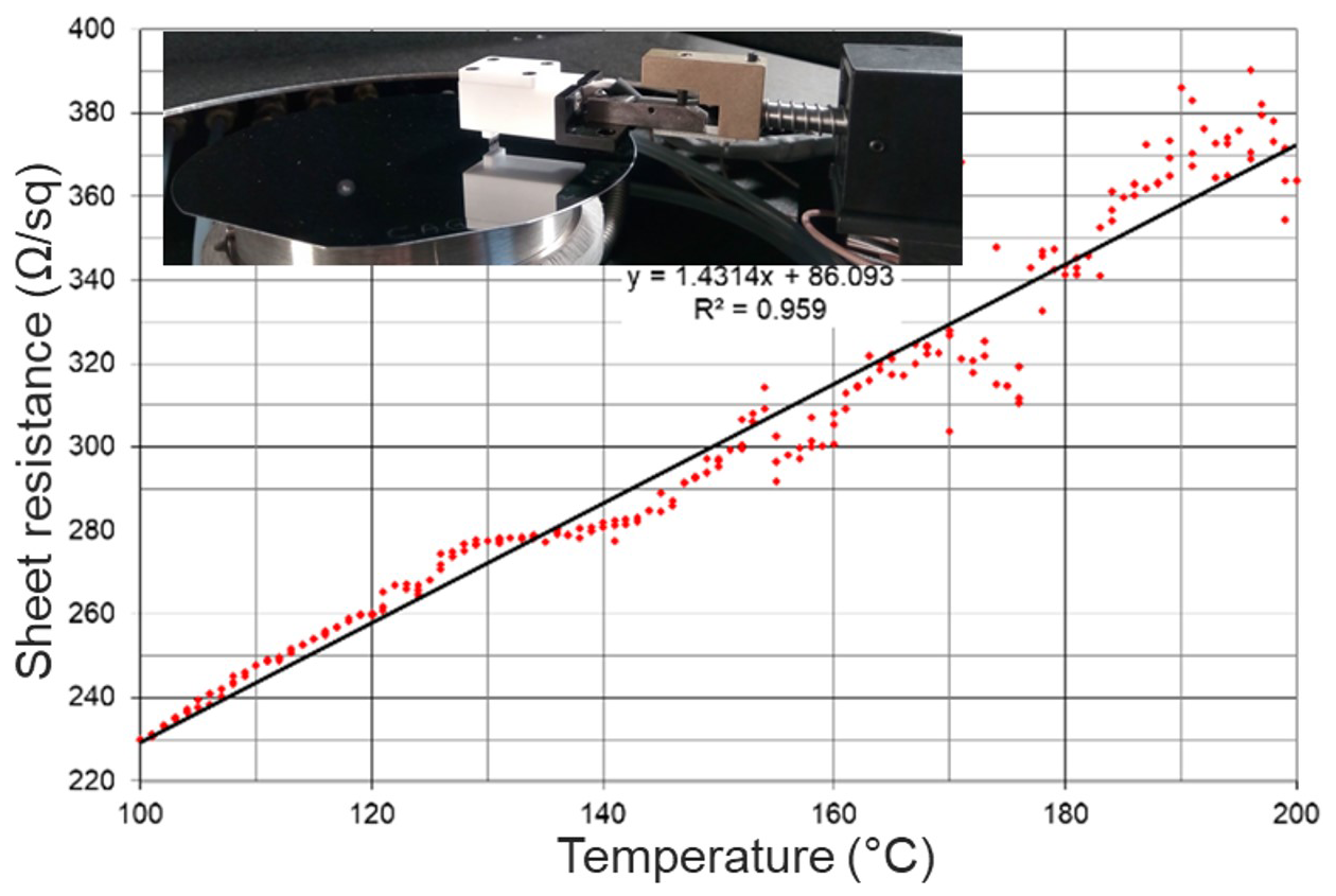
Figure 2Sheet resistance variation of a-Si: H(B) as a function of temperature. Inset: picture of the experimental setup.
This value is 1 order of magnitude higher than the TCR of platinum ( K−1) (Belser et al., 1959). Regarding the heating element, we have chosen titanium nitride (TiN) for its CMOS compatibility; affinity with amorphous silicon for accessing electrical contacts; and relatively low resistivity of Ωcm, allowing us to reach ∼200 °C with 3 V across the resistor.
3.1 Manufacturing technology
TCD sensor chips are micro-fabricated in our clean-room facility by bonding two 200 mm diameter silicon wafers with a dry polymer (SINR, Shin-Etsu) at 180 °C. The bottom wafer incorporates the sensing elements and electric tracks; fluidic channels conveying the gas to be analysed to the sensing elements are etched into the top wafer. The process flow on both wafers involves approximately 100 manufacturing steps. First, a 50 nm thick thermal silicon oxide is grown on the 725 µm thick bottom silicon wafer. A 300 nm thick silicon nitride (SixNy) layer is then deposited by plasma-enhanced chemical vapour deposition (PECVD) at 300 °C. A stepper mask is used to form conductive wires made of TiN and a-Si: H(B) to ensure heating and temperature probing, respectively (see Fig. 3). A 300 nm TiN layer is deposited at 100 °C by means of physical vapour deposition (PVD), while the 300 nm thick a-Si: H(B) layer is deposited at 388 °C by means of chemical vapour deposition (CVD). Another 300 nm thick layer of silicon nitride is deposited before etching the whole stack by means of a deep reactive ion etching procedure (DRIE, also known as a Bosch process): first, an anisotropic etching forms rounded square holes perpendicularly to the wafer's surface, resulting in a net-shaped structure called the membrane. Then, an isotropic etching isolates the membrane from the substrate by forming an underlying cavity of ∼100 µm depth. The membrane holds thanks to arms anchored to the substrate. These also allow electrical routing from the sensing and heating elements. For electrical contacts, an adhesion layer of Ti TiN (10 nm 50 nm) is deposited by means of PVD at 100 °C, and then a 650 nm thick aluminium pad is established by means of PVD at 200 °C.
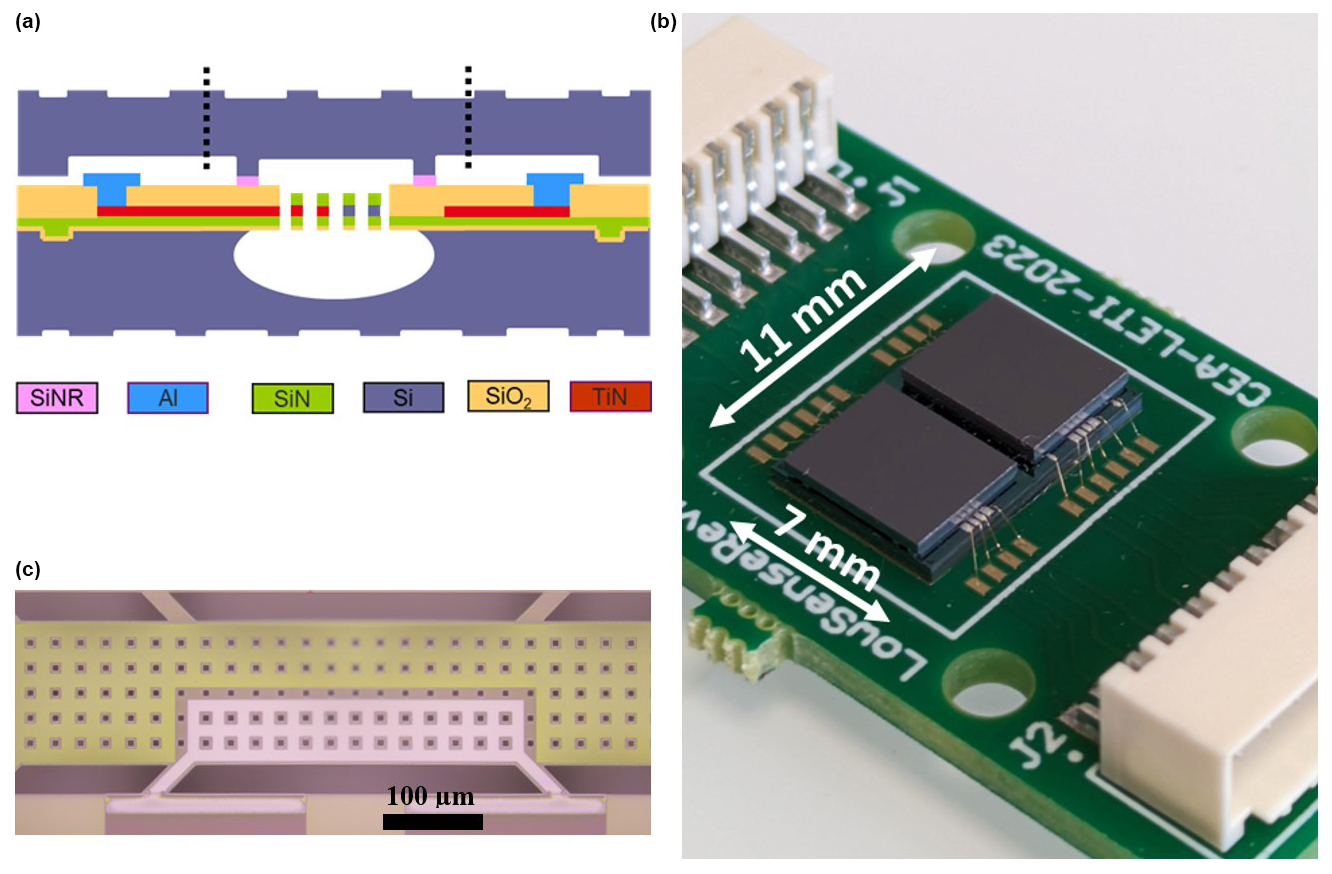
Figure 3TCD manufacturing and assembly. (a) Schematic of the material stack constituting the TCD die. (c) Magnified optical view of the suspended SixNy membrane with a-Si: H(B) sensing element (light violet) and TiN heating element (bronze). (b) Picture of a TCD die wire-bonded to its PCB.
Fluidic channels ensuring gas diffusion to the suspended membrane are etched by DRIE in the top wafer. The analysis and reference chambers have distinct caps to prevent any gas exchange between the chambers in case of imperfect hermeticity of the sealing bond. Two kinds of caps have been designed, depending on the use of the chip. For GC applications, the caps for the reference and analysis chamber are identical, as depicted in Fig. 4.
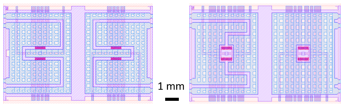
For measurements with a standalone gas sensor, however, the reference cap is different: it is a simple sealed cavity on top of the two membranes to define a closed volume of constant gas composition. In this variant, an additional external seal is added to prevent any leakage.
Once the wafers are fully processed, they are blade diced on a 7122 ADT machine. The dicing procedure involves two main steps: first, a partial dicing along the vertical axis through the cap wafer is carried out in order to release the electrical contacts (Fig. 3, top left, dotted black lines). At this stage, electrical probing tests can be performed to evaluate the electrical resistance values and the homogeneity across the wafer for the sensing and heating elements. Then, a full cut along the horizontal axis through the two bonded wafers is done. It is followed by a partial vertical cut, leaving a safety margin to prevent any water infiltration into the chambers. Finally, individual dies are manually separated before picking the dies for wire bonding. The die to be wire-bonded is first glued onto a dedicated printed circuit board (PCB) using UV15X-2 glue from Masterbond. At this stage, fused silica capillaries are inserted in the four fluidic ports of the chips with a GC cap variant. Capillaries (Molex, Polymicro Technologies TSP100170) are glued to the die using an epoxy glue (EPO-TEK 730) cured at 80 °C for 2 h. Then the 16 electrical pads (4 heating wires, 4 temperature-sensing wires) are connected electrically to the corresponding bonding pads on the PCB using a wire-bonding machine (TPT HB16) in ball-bonding mode at 80 °C, with a 25 µm diameter pure-gold wire (Fig. 3, right). Finally, a glob top resist (Masterbond, UV15X-2) is applied onto the gold wires to protect the electrical contacts. Once mounted onto the dedicated PCB, the silicon die can be connected to an in-house electronic circuit. These driving electronics are able to apply the same voltage to the four TiN heating elements in order to thermalize the whole membrane. At the same time, it applies a bias voltage VBIAS to the Wheatstone bridge composed of four a-Si: H(B) temperature-sensing elements and measures the output signal . These driving electronics are linked to a PC with a LabVIEW interface for analysis sequence programming and data retrieval.
3.2 Results and discussion
3.2.1 GC configuration
Our TCDs were tested on a commercial GC system (Agilent 7890A) using a commercial GC capillary column (Supelco 28471-U; 5 m length, 250 µm internal diameter, 0.25 µm thick; DB-5MS phase) as depicted in Fig. 5. The µTCD die mounted on the PCB was inserted into the GC oven, while its driving electronics were kept outside. Connections between the TCD chip capillaries and the GC system were ensured by external unions (VICI, Valco fittings). The carrier gas was helium. A volume of 50 µL of a pure equivolumic mixture of BTEX (benzene, toluene, ethyl-benzene, and o-xylene) was injected for the different measurements, with a split ratio of 1:100 and an inlet pressure of 8 to 10 psi. The injected mixture first flows through the reference chamber and then to the column. Separated analytes then flow through the analysis channel before being detected by the commercial GC FID used for reference purposes. Figure 5 shows a typical chromatograph obtained in these conditions. The four BTEX compounds are detected in this elution order by the amorphous-silicon and platinum TCD sensors and produce well-resolved peaks.
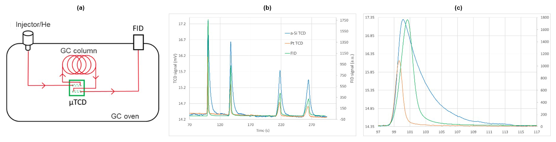
Figure 5GC configuration setup and typical chromatograms. (a) Schematic of the experimental setup. (b) Typical chromatogram obtained for a BTEX mixture (in this elution order) with the amorphous-silicon TCD, conventional platinum TCD, and FID. (c) Magnification of the first chromatographic peak (i.e. benzene).
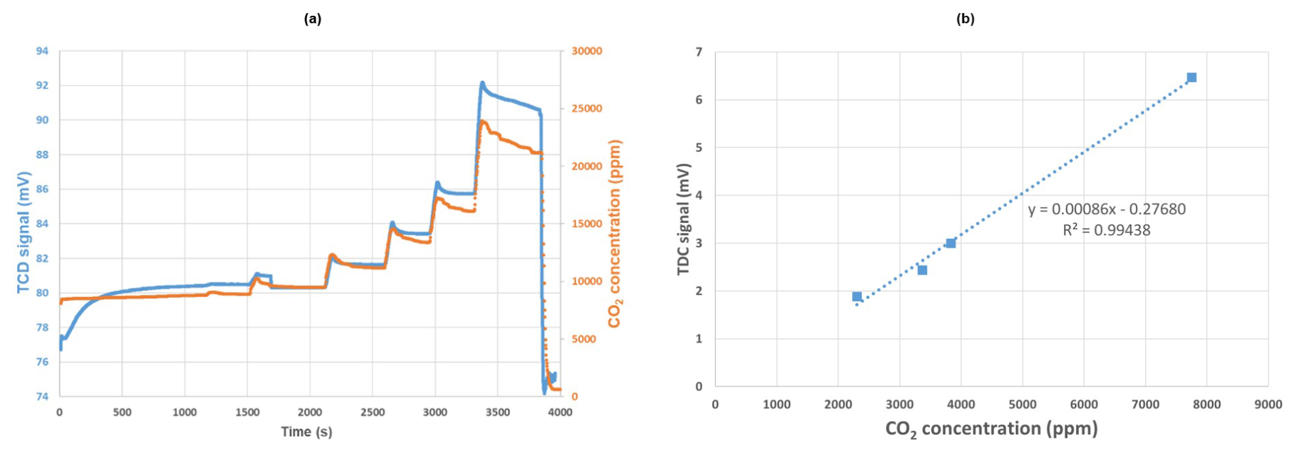
Figure 6Amorphous-silicon TCD signal and CO2 concentration variations. (a) Recording of the TCD signal (blue) and CO2 concentration from a Sensirion SCD30 sensor (orange). (b) TCD signal as a function of CO2 concentration variations.
In order to compare the performances of amorphous-silicon and platinum TCD chips, a sequence of three injections has been recorded for several chips in the same conditions. Each chromatographic peak recorded with the TCD sensor is normalized in relation to the corresponding peak obtained with the FID. Two different criteria are used to compare the TCD technologies: the maximum intensity of the normalized peak and its area. Values are averaged between the four peaks and three sequences. Noise is measured as the standard deviation of the signal averaged for 30 s away from any peak, and this is averaged between sequences. Finally, the two criteria are divided by the noise average to compare the signal-to-noise ratio values. The obtained values are presented in Table 1.
Table 1Performance comparison between platinum and amorphous-silicon TCDs in GC configuration. Bold values represent the values of two criteria used to compare the two technologies. They are obtained by doing mathematical operations on the non-bold values. For normalized peak-intensity-to-noise ratio, the formula is normalized peak-intensity average divided by noise average. For normalized peak-integral-to-noise ratio, the formula is peak-area average divided by noise average.
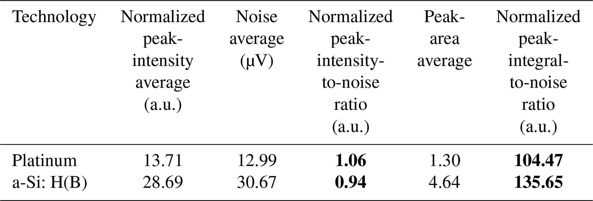
Depending on the criterion considered, amorphous-silicon technology is slightly better or worse than the platinum technology (−10 % for peak intensity; +30 % for peak area); however, there is no significant change in performance between the two technologies. The discrepancy between the two criteria can be better explained by looking at the magnified chromatographic peak in Fig. 5. Indeed, the peak recorded by the amorphous-silicon TCD exhibits a long decaying tail compared to the FID and platinum TCD peaks. Such a peak broadening implies a decrease in the maximum peak value while almost maintaining its area value. This observation is consistent with the opposite results obtained with the two comparison criteria. The peak broadening cannot be attributed to either the GC column or dead volumes in the TCD die as the peaks retain their sharpness when going through the FID placed after the TCD. Although not fully understood and still under investigation, this phenomenon could be linked to the sensor architecture as the temperature-sensing element is indirectly heated, contrarily to the platinum wire.
3.2.2 Standalone configuration
TCDs can be used as standalone gas sensors without the need for a GC system, as reported by Bourlon et al. (2018). Indeed, in specific conditions, i.e. in a gas sample mixture whose nature in terms of the different analytes is known, with one analyte in excess and with n other analytes reaching amount of tens of ppm and above, it is theoretically possible to estimate the analyte concentrations with n measurements at different temperatures and a careful calibration step. For purposes of comparison with standard platinum TCDs, we focused on the measurement of CO2 concentration variations in air. To perform such measurements, the TCD and its driving electronics are placed inside a hermetic chamber with an inlet and outlet, together with a reference CO2 concentration sensor (Sensirion SCD30). The outlet is left open, while the inlet is fed by a home-made gas mixer made up of mass flow controllers (MFCs) controlled by a LabVIEW programme. The gas composition can be adjusted, and the flow rate is maintained at a constant value of 10 mL min−1. The gas in the chamber diffuses passively into the TCD analysis channel and SCD30 sensor.
Figure 6 illustrates the measurement of the CO2 variations in the presence of H2O (35 % relative humidity) and synthetic air (80 % N2 + 20 % O2). The TCD sensor is able to reproduce the CO2 concentration variations observed on the CO2 reference sensor and shows a good linearity, with a coefficient of determination R2 of 0.994. Moreover, we have compared the sensor with conventional platinum TCDs in the same experimental conditions. As shown in Table 2, these sensors are almost 8 times more sensitive to CO2 variations than conventional platinum sensors, as expected from the TCR ratio of 8.3 between these two materials. However, they are also more sensitive to noise (noise being measured by averaging the TCD signal for 30 s in the absence of any temperature, humidity, or CO2 concentration variation), resulting in a signal-to-noise ratio that is 4 times better than that of the platinum TCDs. In the case of CO2, the extrapolated limit of detection for 3σ is equal to 13 ppm.
Table 2Comparison of the conventional platinum TCD technology with the a-Si: H(B)/TiN architecture in standalone configuration.
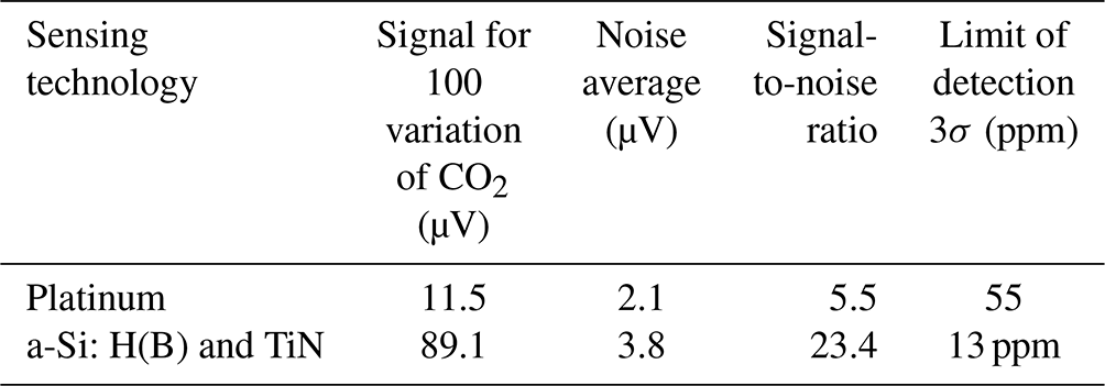
TCDs composed of a titanium nitride heating wire and an amorphous-silicon temperature-sensing wire were conceived, fabricated, and characterized. Boron-doped amorphous silicon was chosen for its CMOS compatibility and high TCR, which we measured to be K−1. Such double-wire TCDs show similar performances compared to conventional platinum TCDs when coupled to a GC system, albeit producing a peak broadening that is not yet fully understood. Therefore, further investigations and design modifications with the aim of using these sensors as GC detectors are needed. However, in a standalone configuration, they bring about a 4-fold improvement in the signal-to-noise ratio and a theoretical limit of detection (3σ) for CO2 in air that is as low as 13 ppm, paving the way towards low-cost, sensitive, portable air quality monitoring systems.
Data are available upon request.
AT and JBT conceived the TCD chips. JBT fabricated and diced the TCD chips. AT and MB assembled the TCD dies on PCBs. AT, FR, and MJ conceived the experiments. AT, FR, and MB carried out the GC experiments. AT and MB performed the standalone experiments. AT and MB processed the data. AT prepared the paper, with contributions from all of the co-authors.
The contact author has declared that none of the authors has any competing interests.
Publisher's note: Copernicus Publications remains neutral with regard to jurisdictional claims made in the text, published maps, institutional affiliations, or any other geographical representation in this paper. While Copernicus Publications makes every effort to include appropriate place names, the final responsibility lies with the authors.
This article is part of the special issue “Eurosensors 2024”. It is a result of the EUROSENSORS XXXVI, Debrecen, Hungary, 1–4 September 2024.
The authors wish to thank Emilie Lefrançois for her help with the driving-electronic LabVIEW interface, as well as Jean-François Beche for designing the driving electronics and TCD chip PCBs. Alexandre Teulle wishes to thank Jean Rottner for his help with the four-probe sheet resistance measurements.
This work was funded by a CBRNE grant from the French government. Results can be published, but we cannot disclose the software code for confidentiality reasons due to the nature of the funding.
This paper was edited by Gabriele Schrag and reviewed by two anonymous referees.
Belser, R. B. and Hicklin, W. H.: Temperature coefficients of resistance of metallic films in the temperature range 25 to 600 °C, J. Appl. Phys., 30, 313–322, https://doi.org/10.1063/1.1735158, 1959.
Berndt, D., Muggli, J., Wittwer, F., Langer, C., Heinrich, S., Knittel, T., and Schreiner, R.: MEMS-based thermal conductivity sensor for hydrogen gas detection in automotive applications, Sens. Actuat. A, 305, 111670, https://doi.org/10.1016/j.sna.2019.111670, 2020.
Bourlon, B., Pham-Ho, A., Beche, J. F., and Constantin, O.: Feasability of a thermal conductivity based CO2 and humidity low cost sensor, in: 22nd International Conference on Miniaturized Systems for Chemistry and Life Sciences, Kaohsiung, Taiwan 11–15 November 2018, 2018.
Cho, W., Kim, T., and Shin, H.: Thermal conductivity detector (TCD)-type gas sensor based on a batch-fabricated 1D nanoheater for ultra-low power consumption, Sens. Actuat. B, 371, 132541, https://doi.org/10.1016/j.snb.2022.132541, 2022.
De Graaf, G., Prouza, A. A., Ghaderi, M., and Wolffenbuttel, R. F.: Micro thermal conductivity detector with flow compensation using a dual MEMS device, Sens. Actuat. A, 249, 186–198, https://doi.org/10.1016/j.sna.2016.08.019, 2016.
Gardner, E. L., Gardner, J. W., and Udrea, F.: Micromachined thermal gas sensors – A review, Sensors, 23, 681, https://doi.org/10.3390/s23020681, 2023.
Hinshaw, J. V.: The thermal conductivity detector, LC GC Europe, 19, 344–351, 2006.
Kaanta, B. C., Chen, H., Lambertus, G., Steinecker, W. H., Zhdaneev, O., and Zhang, X.: High sensitivity micro-thermal conductivity detector for gas chromatography, in: IEEE 22nd International Conference on Micro Electro Mechanical Systems, 25–29 January 2009, Sorrento, Italy, 264–267, https://doi.org/10.1109/MEMSYS.2009.4805369, 2009.
Ketroussi, K., Cherfi, R., Seba, H. Y., Tata, S., Chabane, L., Ozyuzer, L., and Rahal, A.: Study of boron doped amorphous silicon lightly hydrogenated prepared by DC magnetron sputtering for infrared detectors applications, Infrared Phys. Technol., 113, 103556, https://doi.org/10.1016/j.infrared.2020.103556, 2021.
Legendre, O., Ruellan, J., Gely, M., Arcamone, J., Duraffourg, L., Ricoul, F., Alava, T., and Fain, B.: CMOS compatible nanoscale thermal conductivity detector for gas sensing applications, Sens. Actuat. A, 261, 9–13, https://doi.org/10.1016/j.sna.2017.04.036, 2017.
Mahdavifar, A., Navaei, M., Hesketh, P. J., Findlay, M., Stetter, J. R., and Hunter, G. W.: Transient thermal response of micro-thermal conductivity detector (µTCD) for the identification of gas mixtures: An ultra-fast and low power method, Microsyst. Nanoeng., 1, 1–7, https://doi.org/10.1038/micronano.2015.25, 2015.
Pecsar, R. E., DeLew, R. B., and Iwao, K. R.: Performance of a reduced volume thermal conductivity detector, Anal. Chem., 45, 2191–2198, 1973.
Peng, Y., Bulbul, A., Noh, S., Khan, S. U. H., Kim, K. H., and Kim, H.: A Graphene-Based Thermal Conductivity Detector for Low Power Gas Detection, in: IEEE 34th International Conference on Micro Electro Mechanical Systems (MEMS), 25–29 January 2021, Gainesville, FL, USA, 787–790, https://doi.org/10.1109/MEMS51782.2021.9375329, 2021.
Regmi, B. P. and Agah, M.: Micro Gas Chromatography: An Overview of Critical Components and Their Integration, Anal. Chem., 90, 13133–13150, https://doi.org/10.1021/acs.analchem.8b01461, 2018.
Struk, D., Shirke, A., Mahdavifar, A., Hesketh, P. J., and Stetter, J. R.: Investigating time-resolved response of micro thermal conductivity sensor under various modes of operation, Sens. Actuat. B, 254, 771–777, https://doi.org/10.1016/j.snb.2017.07.142, 2018.
Sun, J., Cui, D., Chen, X., Zhang, L., Cai, H., and Li, H.: Design, modeling, microfabrication and characterization of novel micro thermal conductivity detector, Sens. Actuat. B, 160, 936–941, https://doi.org/10.1016/j.snb.2011.09.006, 2011.
Sun, J., Chen, T., Tan, T., Wang, D., Zhu, X., Zhang, X., Peng, H., and Luan, Z.: Fabrication and characterization of a novel micro-thermal conductivity detector for monitoring small-molecule gases, IEEE Sens. J., 20, 11115–11121, https://doi.org/10.1109/JSEN.2020.2997818, 2020.
Tan, T., Sun, J., Chen, T., Zhang, X., and Zhu, X.: Fabrication of Thermal Conductivity Detector Based on MEMS for Monitoring Dissolved Gases in Power Transformer, Sensors, 20, 106, https://doi.org/10.3390/s20010106, 2020.
Zhou, X. F., Zhang, H., Yan, H., He, C. L., Lu, M. H., and Hao, R. Y.: Giant temperature coefficient of resistance in Co-doped ZnO thin films, Appl. Phys. A, 114, 809–812, https://doi.org/10.1007/s00339-013-7665-8, 2014.