the Creative Commons Attribution 4.0 License.
the Creative Commons Attribution 4.0 License.
 | 19 Mar 2021
Novel, low-cost device to simultaneously measure the electrical conductivity and the Hall coefficient from room temperature up to 600 °C
Robin Werner
Jaroslaw Kita
Michael Gollner
Florian Linseis
Ralf Moos
A novel measurement device for simultaneous high temperature measurements of the electrical conductivity and the Hall coefficient has been developed. Simulations were used to design a suitable screen-printed planar platinum heating structure that generates temperatures of up to 600 ∘C by Joule heating. Simulations of the temperature distribution have been validated using thermal imaging. With the hardware setup of two permanent magnetic yoke systems with a magnetic flux density of ±760 mT, the electrical conductivity and the charge carrier densities of a silicon wafer and a gold film were measured, as examples of a typical semiconductor with low charge carrier densities but high mobility and a metal representing materials with very high charge carrier densities but moderate mobilities, respectively. Measurements were compared with data from the literature to validate the functionality of the novel, low-cost measurement device.
- Article
(1799 KB) - Full-text XML
- BibTeX
- EndNote


Electrical transport parameters such as electrical conductivity, charge carrier density, and Hall mobility play an important role in material characterization. To meet the application needs, measurements in a wide temperature range are required. The method of van der Pauw (1991) simplifies the electrical characterization, but the availability of commercial measuring instruments for high temperature characterization, especially for measurements within a magnetic field, is limited. There are only a few instruments on the market for this purpose. The commercial measuring instruments, and those described in the literature, can be divided into two categories. On the one hand, one can distinguish between devices with an electromagnet or permanent magnet and, on the other hand, devices with an actively heated sample holder or a passively heated one, where the surrounding atmosphere is heated, e.g., in a furnace. Examples of the latter are given by Lake Shore Cryotronics, Inc. They offer measurements of up to 1000 ∘C (Lake Shore Cryotronics, Inc., 2019); however, the electromagnet and the furnace make the instruments very costly. Many research groups such as those listed in the literature (see, e.g., Dauphinee and Mooser, 1955; Wood et al., 1984; Fleischer and Meixner, 1994; Moos et al., 1995) or even NASA's Jet Propulsion Laboratory (JPL) setup (McCormack and Fleurial, 1991) also use electromagnets, either with furnaces or with heating wires around the measurement chamber, reaching maximum temperatures of 1000 to 1100 ∘C. The combination of an electromagnet and actively heated sample holders is shown by Caltech (California Institute of Technology) and Aarhus University (600 ∘C; Borup et al., 2012).
Expensive electromagnets can be replaced by permanent magnets, if one is aware of several disadvantages. The magnetic flux density is usually much lower and cannot be easily varied. Furthermore, they cannot be operated by using radiative heaters, as exceeding the Curie temperatures leads to demagnetization. Some commercial measurement instruments with permanent magnets use active heating of the sample holder for this purpose. In these cases, the sample holders are made of a material with good thermal conductivity and are heated by external heat sources. The maximum measurement temperatures for these instruments, as specified by the manufacturer, are 500 ∘C (Ecopia, 2009) and 527 ∘C (MMR Technologies, 2013). The disadvantage of externally heated and good thermal conductive materials is clearly shown by the research group of Adnane et al. (2016). In their work, the sample holder is based on a brass chuck with two embedded cartridge heaters with a power of 300 W each. The two heaters were controlled to a temperature of 700 ∘C. Despite the good thermal conductivity of the brass chuck, a temperature of only 510 ∘C could be measured on the sample. Another example of such a setup is shown by Gunes et al. (2017). This research group utilizes an AlN plate as a sample holder. It is connected to a copper furnace, reaching sample temperatures of 377 ∘C. The special feature of this system is the use of a cylindrical Halbach array, a special arrangement of permanent magnets with a homogeneous magnetic field on the inside and no magnetic field on the outside of the cylinder.
A further commercial measuring instrument with a different heating principle provides temperature control via the expansion of non-ideal gases by the Joule–Thomson effect and can reach temperatures of up to 457 ∘C in a vacuum (Nanomagnetics Instruments, 2020). Another way of heating the sample is the use of Joule's heating by integrated metal thick films on the sample holder. An example of this, with a maximum temperature of maximum 177 ∘C, has been investigated by Linseis et al. (2016).
The need for measuring devices, as described above, and the distinct disadvantages of existing instruments triggered the development of a novel, low-cost measurement system that includes the use of permanent magnets and an active heating of the sample up to 600 ∘C.
A schematic representation of the basic idea of the novel measurement device is shown in Fig. 1. The measuring setup consists of two components, namely a sample holder and a measuring chamber with a movable magnetic yoke system of permanent magnets. The basic structure of the new sample holder is made of a ceramic substrate. In the center of the reverse side of the sample holder there is a meander-shaped screen-printed heating structure made of platinum. It is intended to heat the sample area on the top side to a desired temperature of up to 600 ∘C by Joule's heating. The planar heating structure has four separate supply lines. A direct current (DC) voltage is applied to the two inner leads, so the tip of the sample holder heats up to 600 ∘C due to the resistance in the heating structure. The resistance within the heated meander-shaped structure (and, hence, in the sample area) can be measured directly via the four leads by a four-wire technique. Due to the one-time calibration with the help of a thermal imaging camera, an exact temperature can be assigned to each resistance since a homogeneous temperature distribution is achieved in the sample area. On the reverse side, gold leads are also applied. They lead to the electrodes on the top side. Screen-printed connection pads for a conventional card edge connection allow for easy connection to the measuring electronics and facilitate sample changing.
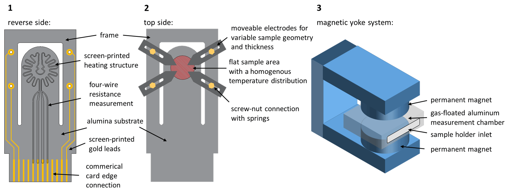
Figure 1Schematic representation of the new measurement device. (1) Sample holder, with a thick film heating structure and card edge connection on the reverse side. (2) Top side, with a sample area having a maximum diameter of 12.7 mm and four moveable electrodes for Hall and conductivity measurements, according to van der Pauw's method. (3) Magnetic yoke system with permanent magnets and a gas-flushed aluminum measurement chamber.
On the top side of the sample holder, there is the later sample area. Here, the temperature distribution is homogeneous. The four movable electrodes with which the sample is to be contacted are electrically connected on the underside via a screw–nut combination. An additional integrated spring allows the electrical contacts to be height adjustable and allows the application of sufficient contact pressure. The electrodes themselves have a guide groove and, thus, a large freedom of movement, allowing samples of any geometry between 5 to 12.7 mm diameter to be contacted within the red marked sample area, according to van der Pauw's method. To protect the springs from softening, the electrodes should be made of a material with low thermal conductivity to decrease the heat flow between the electrical contact of the sample and the spring. In addition, the springs are located on a separate frame of the sample holder to reduce the heat flow.
A magnetic yoke system of permanent magnets is a further part of the device. Between the magnets, the sample holder is mounted inside a fixed, gas-flushable aluminum measurement chamber. The homogeneity and strength of the magnetic field are adjusted by the diameter of the permanent magnets and the distance between the yokes, taking the Curie temperature into consideration to prevent the weakening of the magnetic field at higher measurement temperatures.
2.1 Consideration for substrate materials selection
In order to find the most suitable substrate material, a few boundary conditions have to be defined. Of the three criteria, one that needs to be fulfilled is the use of springs to achieve flexibility in the sample geometry. Furthermore, the sample holder should be able to be connected via commercial card edge connectors for easy handling, which means that the temperatures should not exceed 150 ∘C in this area; otherwise, this could lead to melting of the connector. Furthermore, due to the horizontal positioning of the sample holder, the connection to the card plug is the only fixture, which is why it must have the necessary strength. As a final criterion, a temperature of 600 ∘C should be achieved with the applied screen-printed heater layer structures. Some important data, with respect to the selected materials, are listed in Table 1 for this purpose.
Table 1Comparison of the mechanical and thermal properties of different commercially available substrate materials. Parameters were taken from the manufacturers' data sheets and literature (DuPont, 2011; KERAFOL Keramische Folien GmbH & Co. KG, 2020; MARUWA Co., Ltd., 2019; Verband der Keramischen Industrie e.V., 1999). The thermal conductivity for Al2O3 is calculated from Kita et al. (2015).

All of the substrates listed could be used to produce a screen-printed heater, and all materials have sufficient strength to be horizontally clamped onto a card edge connector. LTCC and 3-YSZ show the lowest thermal conductivity of all the materials, resulting in a low heat flow within the sample holder. The use of card edge connections and spring-loaded electrical contacts would probably be possible with these materials. The material of 3-YSZ also has a very high maximum flexural strength, which allows the sample holder to be subjected to high thermally induced stresses. Unfortunately, YSZ becomes oxide ion when conducting at high temperatures, which may affect the measurements (Badwal, 1992). The use of LTCC is, furthermore, made risky by the high temperatures, as the operating temperature of 600 ∘C is not far from the sintering temperature of 850 ∘C. AlN would probably be the best-suited material for the temperature distribution inside the sample area due to its high thermal conductivity, but this also makes the use of a card edge connector and spring-loaded contacts difficult. Al2O3, on the other hand, seems to meet all the requirements. The temperature-dependent thermal conductivity can enable the use of springs and card edge connections through careful design. Even with a maximum flexural strength of 500 MPa, thermal stress could be withstood at a temperature of 600 ∘C.
3.1 Temperature distribution
The new sample holder design and the heating structure development for a homogeneous temperature distribution within the sample area were simulated using the FEM software COMSOL Multiphysics®. The basic structure of the sample holder is a 630 µm thick Al2O3 substrate with a temperature-dependent thermal conductivity λ(T), according to Kita et al. (2015), which is given in Eq. (1) as follows:
On the reverse side of the substrate, a planar screen-printed heating structure was applied to generate a homogenous temperature distribution on the top side for Hall measurements. All thermal parameters used in the simulation are listed in Table 2.

The resistivity and the temperature coefficient of the resistance of platinum were taken from the data sheet of the paste manufacturer. Parameters for convection and radiation were determined by preliminary tests. For this purpose, screen-printed heating structures were fabricated on Al2O3 and recorded at different temperatures with a thermal imaging camera. Subsequently, the convection and radiation boundary conditions could be determined by adjusting the simulation. On the upper side of the sample holder, a circular sample area was indicated within which the material sample to be characterized should be positioned later. The simulation was carried out in a steady state. The circular sample area was evaluated. The results for a temperature of 600 ∘C are shown in Fig. 2.
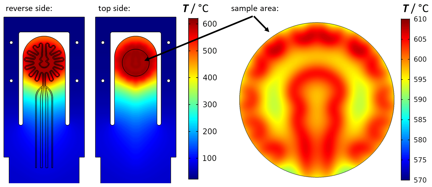
Figure 2Simulation of the temperature distribution of the new sample holder. A screen-printed platinum structure is used to generate the temperature via Joule's heating. On the top side, the sample area is drawn, and a detailed representation of the temperature distribution is given.
The simulation shows the temperature distribution within the entire sample holder. The meander-shaped heater structure on the reverse side of the sample holder can generate a temperature of up to 600 ∘C on the surface of the top side of the Al2O3 substrate by Joule's heating. The lower thermal conductivity of Al2O3 at high temperatures reduces the heat flow and offers the possibility of a locally heated zone. The increasing thermal conductivity at decreasing temperatures of Al2O3, on the other hand, provides a faster cooling effect on the rest of the sample holder, which allows the use of card edge connectors, even at measurement temperatures of 600 ∘C. The integrated frame, on which the electrical leads for the van der Pauw measurements are located, ensures that the temperature in the area of the vias is minimized, thus allowing the use of springs and, thus, a flexible sample geometry. Figure 2 also shows a detailed view of the temperature at the sample area. Within the circular area with a diameter of 12.7 mm, the maximum temperature difference is ±7 K. Joule's heating generates the highest temperature above the planar heating tracks and a small temperature drop between the conductor paths. These small temperature differences cannot be prevented with this construction. Usually, even such small temperature differences lead to thermoelectric voltages. However, these do not play a role in later measurements, according to ASTM F76-08 (standard test methods for measuring resistivity and Hall coefficient), since thermoelectric voltages are eliminated by reversing the polarity of the currents. Nevertheless, the temperature distribution can be considered as homogeneous within the sample area.
In this simulation, electrodes and vias were not considered because no reliable parameters for the convection and radiation were available. However, a heat flow worth mentioning takes place through the electrodes. This heat flow provides a lower temperature at the contact points, which is also known as the cold finger effect. Based on the measurements, according to the van der Pauw method and the very small, almost punctual electrical contacts required by this, the assumption was made that this effect can be neglected. Due to the thermal constriction at the small contact points, a high thermal resistance can be assumed. This limits the heat flow to the outside, which means that only a small, negligible temperature loss can be expected at the contact point.
3.2 Thermal stress
Additionally, the mechanical stability of the sample holder was simulated. Previous work revealed that the thermal stress can be a limiting factor for screen-printed heaters on ceramic layers (Ritter et al., 2017). The resulting thermal stresses σthermal can be described by Eq. (2), as follows:
where E is the Young's modulus, α the thermal expansion coefficient, and ΔT is the temperature difference. The simulation was carried out in the steady state at a temperature of 600 ∘C within the sample area. To evaluate the maximum thermally induced mechanical stresses that may occur, the von Mises stress is considered. The results are shown in Fig. 3. The thermal expansion of the Al2O3 substrate itself generates a maximum stress of 410 MPa. The result of this simulation shows that temperatures of up to 600 ∘C can be achieved with the new concept since the thermally induced stresses are below the maximum bending stresses of 500 MPa specified by the manufacturer.

Figure 3Simulation of the thermally induced mechanical stress within the sample holder at a temperature of 600 ∘C.
4.1 Sample holder
The heating structure developed from the simulations and the new manufactured sample holder is shown in Fig. 4. A commercial 96 % Al2O3 ceramic, with a thickness of 635 µm, serves as a substrate. The platinum heating structure was screen printed and fired at 950 ∘C. The gold tracks and the connection pads were added in a second screen-printing process and were fired at 850 ∘C. On the top side, Inconel electrodes with a guide groove and a curved tip were installed. Inconel is electrically conductive but has a low thermal conductivity, which makes the use of springs at the screw–nut connection through the vias possible. In addition, it is a non-magnetic material, and measurements within the magnetic field are realizable. With these electrodes, samples of any geometry between 5 and 12.7 mm diameter can be electrically contacted and homogeneously heated. The gold connection pads on the reverse side allow using commercially available card edge connections and, thus, connecting easily to the measurement and control electronics.
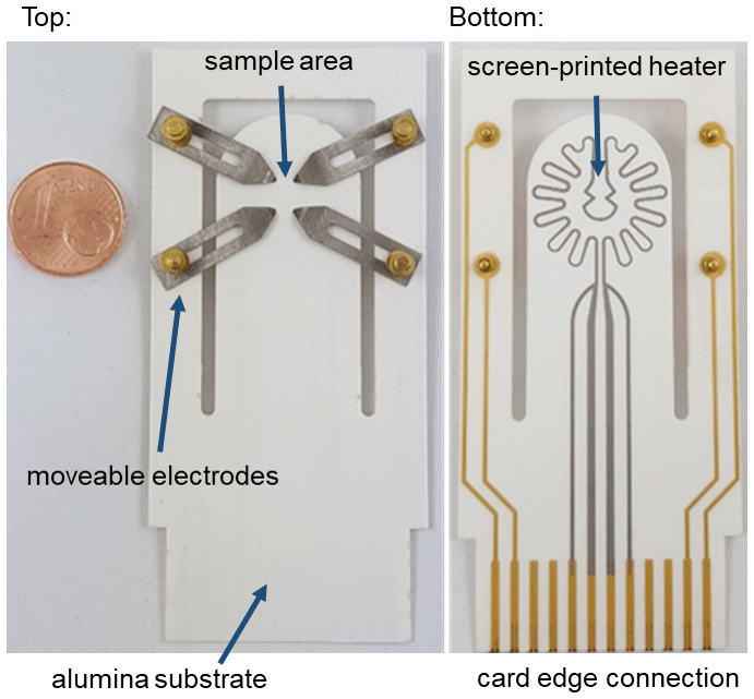
Figure 4Produced sample holder made of an alumina substrate with four movable, spring-mounted Inconel bars for electrical contact on the top side. On the bottom side there is a screen-printed platinum heating structure, gold leads, and connection pads for the card edge connection.
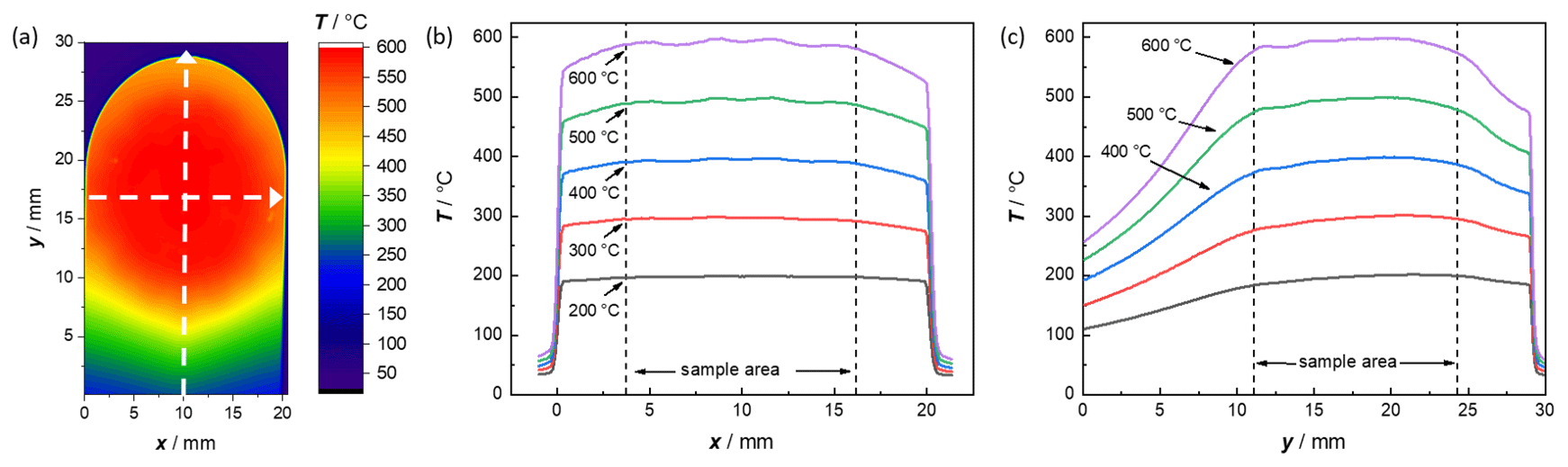
Figure 5Thermal image of the sample area at 600 ∘C. (a) Homogeneous temperature distribution within the sample area (b) Temperature profile along the x axis. (c) Temperature profile along the y axis through the center of the sample area.
4.2 Thermal imaging
The new sample holder concept with the simulated planar heating structure was validated with a thermal imaging camera (VarioCAM® HD). For the experiment, the sample holder was placed in a horizontal position, adjusted by a spirit level, and then the camera was focused on its top side, measuring the temperature within the sample area under a normal atmosphere. A DC voltage was applied to heat the sample holder in 100 ∘C steps up to 600 ∘C. During the thermal imaging, the resistance of the platinum heater was measured with a Keithley 2700 Multimeter, using a four-wire technique, to calibrate the resistance–temperature curve that is used in later measurements. A detailed thermal image of the top side of the sample holder at 600 ∘C is shown in Fig. 5. The thermal image reveals a homogeneous temperature distribution at the sample area and a strong temperature drop between the heated area and area of the electronic card edge connection. The strong temperature drop could already be observed in the simulation shown in Fig. 2. The assumption that the temperature at the connected side is low enough to use commercial card edge connectors was confirmed. Figure 5b and c show the temperature profiles along the x and y axis through the center of the sample area at measurement temperatures of 200 to 600 ∘C. To evaluate the homogeneity of the temperature distribution, the area of the maximum sample size was considered, which is marked by a dotted line (sample area) in the diagrams. The temperature profiles along the x axis already show a homogeneous temperature distribution within the maximum sample area at 200 ∘C. With increasing temperature, small temperature differences become visible. They are, however, even at 600 ∘C, not higher than ±6 ∘C within the sample area. A larger drop in temperature can be observed along the y axis. At a measuring temperature of 600 ∘C, there is a maximum temperature difference of ±12 K within the maximum sample area of 12.7 mm diameter. A reduction in the sample diameter by only 1 mm (i.e., to 11.7 mm), however, would decrease the temperature deviation to a maximum of only ±6 K. To sum up, the concept of the ceramic sample holder with integrated heater could be validated, and the Hall coefficient measurements may be possible (see Sect. 5.2).
In addition, however, the influence of the thermal conductivity and emissivity of the sample should be discussed. The measurement setup and the resistance–temperature calibration only adjust the temperature on the sample holder surface. A sample with a certain thickness will have a different temperature on the sample's upper side, at the electrical contact points, compared to the bottom side, where the calibration was performed. The surface temperature is, thus, dependent on the emissivity and the thermal conductivity of the sample. A high emissivity, which indicates the heat radiation emitted to the environment, also results in lower temperatures on the sample surface. The same holds for the thermal conductivity. For samples with a low thermal conductivity, the heat flow through the sample is reduced, which results in a lower surface temperature. In these cases, the calculated transport parameters may be referenced to a somewhat incorrect temperature. Therefore, a thin sample is preferred to minimize errors.
Furthermore, the sample has an influence on the temperature distribution. It can be assumed that a sample with a different heat capacity, thermal conductivity, or emissivity to Al2O3 may affect the temperature distribution within the sample area and also within the sample itself. This lower temperature homogeneity can lead to the occurrence of thermoelectric voltages and associated measurement errors. However, reversing the polarity of the current eliminates this effect.
Temperatures higher than 600 ∘C cannot be reached with this measurement setup. The reason for this can be seen in Fig. 6. It shows a section of the meander-like platinum heating structure. The substrate cracked at a temperature of about 650 ∘C, which was also indicated by the thermally induced mechanical stresses shown in Sect. 3.2. It can be clearly seen that the previously predicted weak points are accurately reproduced by the cracking pattern. In order to achieve higher temperatures, the thermal stresses have to be reduced. This may be realized by another material with a lower Young's modulus E and a lower thermal expansion coefficient α or by reducing the temperature gradient inside the material by redesigning the heating structures.
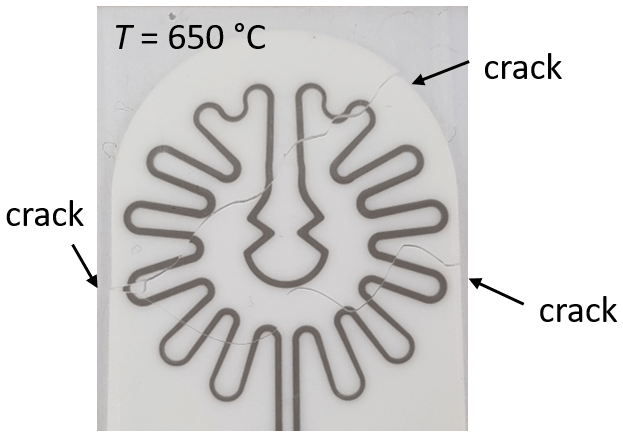
Figure 6Magnified view of the heating meander on the bottom side of the sample holder. The substrate cracked at a temperature of about 650 ∘C.
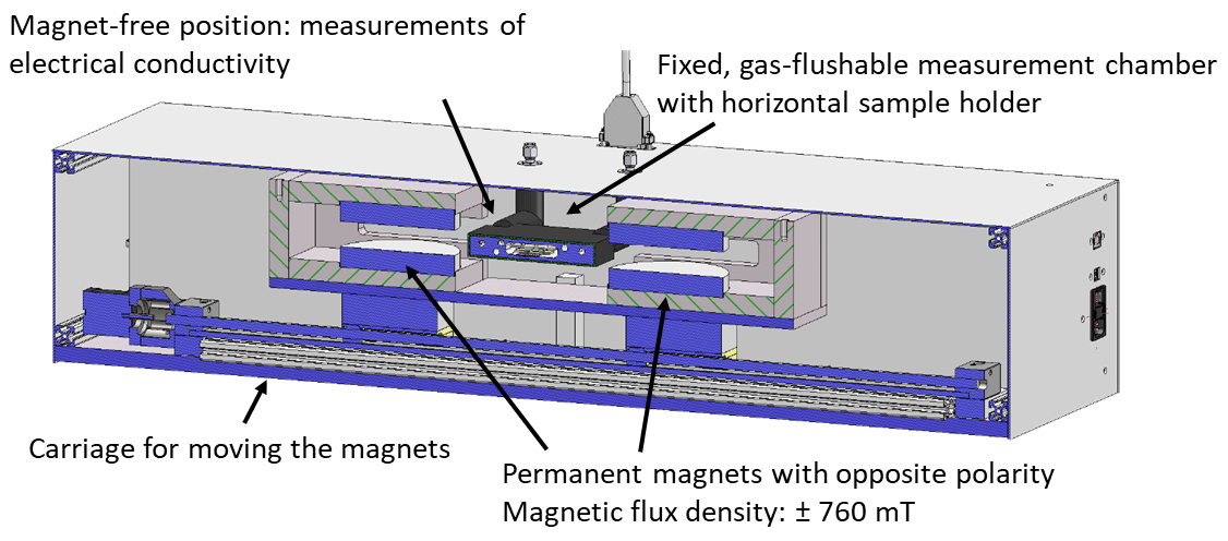
Figure 7Hardware structure showing two movably mounted magnetic yoke systems of permanent magnets on a sledge for measurements without and in positive/negative magnetic fields.
4.3 Hardware setup
The hardware setup for the measurement system is shown in Fig. 7. The system consists of two permanent magnet yokes. The magnets have a diameter of 90 mm and a magnet distance of 20 mm. In this configuration, a homogeneous magnetic flux density of ±760 mT can be generated within the sample area. The influence of the platinum heating structure on the magnetic field can be neglected here since, even at 600 ∘C sample holder temperature, only a small current of 0.5 A is impressed through the narrow cross section of the screen-printed conductor tracks. By mounting the magnets on a sledge, Hall coefficients can be measured with positive, negative, or no magnetic field. The sample holder is connected to the electronics via a card edge connection and installed in a fixed, gas-flushable aluminum measurement chamber. The sample holder and the hardware allow for the determination of the resistivity and the Hall coefficient, according to the van der Pauw method and the guidelines of ASTM International standard F76-08 (ASTM International, 2016).
All measurements were performed inside the measurement chamber under a normal atmosphere and without an external gas inlet. The resistance–temperature calibration described in Sect. 4.2 was used. Due to the horizontal positioning of the sample holder and the associated heat transfer coefficients, hardly any changes in the temperature distribution are expected. Only the temperature inside the measurement chamber may increase. The platinum structure is also affected by the increased ambient temperature, but this has no influence on the temperature of the sample area, since it is controlled by the temperature-dependent four-wire resistance directly under the sample area.
5.1 Electrical conductivity
To verify the new measurement setup, a 200 nm sputtered gold thin film on alumina and a commercial 380 µm float zone silicon wafer with weak boron doping and (100) orientation (CrysTec GmbH) were measured. The gold layer is a rectangular structure that could be contacted directly at the edge using the movable Inconel bars. The silicon-wafer, on the other hand, was previously cut with a laser so that it had a cloverleaf structure. This structure allows a variable contact area and free positioning of the contacts within the individual blades. To measure the resistivity, a constant current was applied by a Keithley 2400 SourceMeter® on two adjacent contacts, and the voltage between the remaining contacts was measured by a Keithley 2182A Nanovoltmeter. The measurement configuration for the exemplary voltage U21,34 can be seen in Fig. 8a. The first two indices represent the contact where the current is applied, and the rear indices stand for the voltage measurement. The contacts were then exchanged to use each of the possible combinations. The measurements were also carried out with a reversed polarity current to compensate for possible offset errors. The raw data of these eight measured voltages, shown in Fig. 8b, are exemplary for a boron-doped silicon wafer sample at a temperature of 500 ∘C and with an impressed current of 10 mA. The voltages (measured with the Nanovoltmeter) are constant with time t. Even a closer look at the voltage U14,23 reveals a fluctuation of less than ±1 µV. The raw data, in this case, prove that the electrical currents through the planar heater on the reverse side do not affect the quality of the measurement.
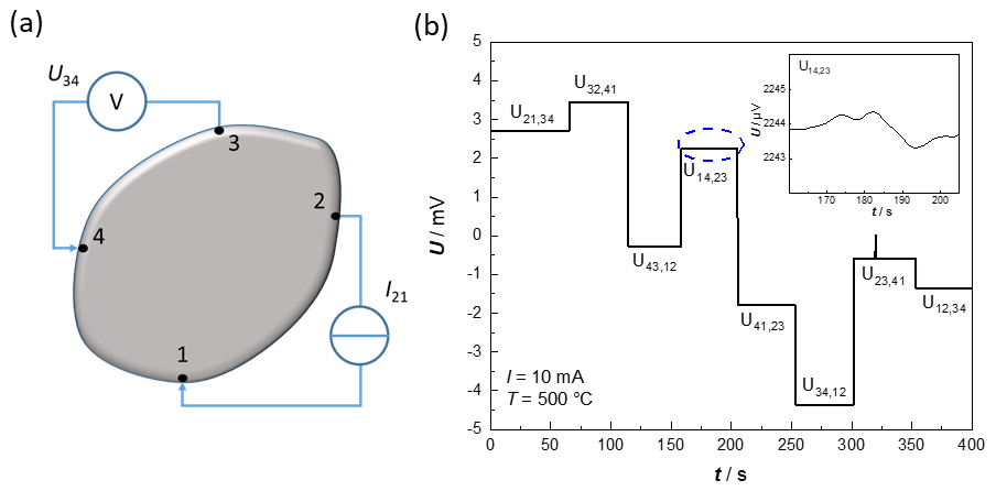
Figure 8Measurement of the electrical conductivity. (a) Exemplary measurement configuration for the voltage U21,34. (b) Exemplary raw data of the measured voltages of a silicon wafer, to determine the electrical conductivity at 500 ∘C, to investigate the influence of the heater.
With the measured voltages U, the sample thickness t, the current I, and the geometry factor f, two resistivities can be calculated from which the average sample resistivity is then calculated. The geometry factors fA and fB are calculated from the voltage ratios QA or QB in Eqs. (5) and (6) and are subsequently determined numerically using Eq. (7), according to the ASTM International standard F76-08, using the van der Pauw method. (ASTM International, 2016)
Figure 9 shows the determined electrical conductivities of the silicon wafer and the gold thin film in an Arrhenius-like representation for temperatures between room temperature and 600 ∘C. The electrical conductivity of the gold thin film (black filled squares) decreases with increasing temperature. This conductivity behavior can be explained by the thermally excited lattice vibrations (phonons) that occur in metals (Kittel, 2018). The boron-doped silicon wafer shows a slight decrease in the electrical conductivity between room temperature and 150 ∘C, since the semiconductor is in the range of impurity exhaustion here. Above 200 ∘C, the electrical conductivity of the slightly p-doped silicon wafer increases exponentially. This can be explained by the thermal generation of electron hole pairs in the region of intrinsic conduction. In addition, a straight line with the intrinsic conductivity, adapted from Morin and Maita (1954), is shown in Fig. 9. The measurements clearly show that the electrical conductivity up to 600 ∘C of silicon can be determined and can also be directly compared with the literature. In addition, the activation energy calculated from the slope of the conductivity was determined, which, at 1.1 eV, also corresponds to the band gap of silicon (Li, 1978; Kittel, 2018).
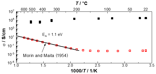
Figure 9Arrhenius-like representation of the measured temperature-dependent electrical conductivity of a gold thin film (thickness 200 nm) and a boron-doped silicon wafer (thickness 380 µm) up to 600 ∘C, with an additional comparison of the intrinsic conductivity of silicon (adapted from Morin and Maita, 1954).
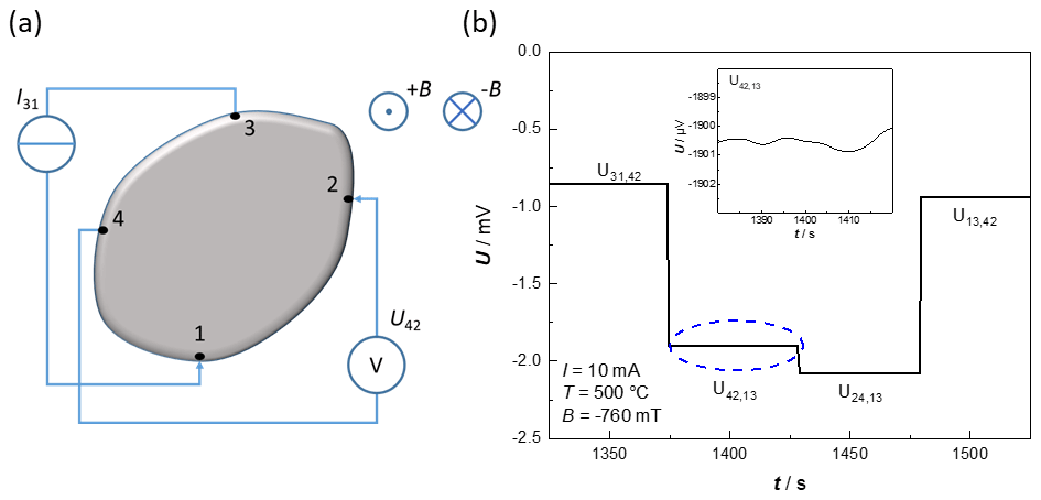
Figure 10Measurement of the Hall coefficient. (a) Exemplary measurement configuration for the voltage U31,42. (b) Exemplary raw data of the measured voltages of a silicon wafer for the determination of the Hall coefficient at 500 ∘C to investigate the influence of the heater.
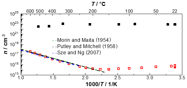
Figure 11Arrhenius-like representation of the charge carrier densities of a gold thin film (thickness 200 nm) and a boron-doped silicon wafer (thickness 380 µm) calculated from the Hall coefficient up to 600 ∘C, with an additional comparison of the charge carrier density adapted from Morin and Maita (1954), Putley and Mitchell (1958), and Sze and Ng (2007).
5.2 Hall effect measurements
To measure the Hall voltages, the currents were applied between two opposite contacts, and the voltages were measured at the remaining contacts. A schematic illustration of the configuration for the voltage U31,42 is shown in Fig. 10a. The measurements were carried out inside a magnet and repeated with an opposite-poled magnetic field. Raw data of the measurements inside the magnetic field (current 10 mA; temperature 500 ∘C; silicon wafer, as described above) are shown in Fig. 10b. As can be seen, the voltage fluctuations are very small, and the Hall voltage UH can be easily determined with this setup. The Hall coefficient RH is calculated by Eqs. (8) and (9), according to the ASTM F76-08, with the magnetic flux density B in Tesla.
If the deviation of both measured Hall coefficients is less than ±10 %, a homogeneous sample can be assumed. The Hall coefficient is then calculated from the average of both measurements and is used to determine the charge carrier density in Eq. (10).
In the case of a dominant type of charge carrier, the charge carrier density can be calculated directly from the Hall coefficient RH with knowledge of the proportionality factor r, which is dependent on the material-specific scattering mechanisms (Schroder, 2006; Pfüller, 1977) and the charge q (−e for electrons and +e for holes, with e being the elementary charge). For silicon, the proportionality factor can be assumed to be (Pearson and Bardeen, 1949), and for gold it is r≈1 (Pfüller, 1977). In the intrinsic region of a semiconductor, electron hole pairs are generated, meaning that both the mobility of holes μp and electrons μn must be considered when calculating the intrinsic charge carrier density ni with Eq. (4) (Pearson and Bardeen, 1949).
Since, in the intrinsic region, the number of holes p can be assumed to be equal to the number of electrons n, and the temperature-dependent mobility of intrinsic silicon can be calculated according to Eqs. (12) and (13), the charge carrier densities in Fig. 11 results (Morin and Maita, 1954; Pfüller, 1977).
The charge carrier density of gold shows the expected temperature-independent course. The number of free electrons is also in the range of the theoretical charge carrier density of 1/cm3, under the consideration of the electron gas model and the assumption of one free electron per gold atom. In contrast, the charge carrier density of silicon shows hardly any change in the range of impurity exhaustion up to a temperature of 200 ∘C. Above 200 ∘C, the intrinsic conduction of silicon begins. The intrinsic charge carrier density increases exponentially with increasing temperature. For comparison, and to prove the functionality of the new measurement system, the intrinsic charge carrier densities are additionally plotted in an adaption from Morin and Maita (1954), Putley and Mitchell (1958), and Sze and Ng (2007). The comparison with the literature and the proof of the intrinsic charge carrier density of silicon with this measurement setup confirm the functionality of this novel measuring device.
Applying FEM simulations, a new ceramic sample holder with a screen-printed planar heater structure was developed. It allows the generation of a homogeneous temperature distribution within a 12.7 mm diameter sample area for conductivity and Hall measurements up to 600 ∘C. Experiments with a thermal imaging camera confirmed the simulation results of the temperature distribution. With the new setup, it is possible to avoid the use of expensive furnaces and, in addition, the use of inexpensive permanent magnets is possible rather than using expensive electromagnets. Electrical conductivity and charge carrier density measurements of gold and silicon wafer confirm the functionality. High temperature measurements of a silicon wafer within the intrinsic region agree well with the literature. The sample holder is constantly being further developed, such as increasing the maximum measuring temperature, measuring more known materials, and adding new functionalities, like the Seebeck coefficient or the thermal conductivity.
All relevant codes presented in the article are stored according to institutional requirements and, as such, are not available online. However, all data used in this paper can be made available upon request to the authors.
RM, JK, MG, and FL created the concept of the project and were responsible for the funding acquisition. Hardware setup was provided by MG and FL. The sample holder, all simulations, the construction, the validation, and the measurement data analysis were done by RW in close discussion with RM, JK, MG, and FL. All authors contributed to the reviewing and editing of the final paper. RM supervised the work.
The authors declare that they have no conflict of interest.
This article is part of the special issue “Sensors and Measurement Science International SMSI 2020”. It is a result of the Sensor and Measurement Science International, Nuremberg, Germany, 22–25 June 2020.
This research has been supported by the Bayerisches Staatsministerium für Wirtschaft und Medien, Energie und Technologie within the scope of the project “LHA –
Hochtemperatur-Messgerät zur Bestimmung der elektrischen
Transporteigenschaften von Materialien” (grant no. ESB-1607-0002//ESB040/001).
This open-access publication was funded
by the University of Bayreuth.
This paper was edited by Eric Starke and reviewed by two anonymous referees.
Adnane, L., Gokirmak, A., and Silva, H.: High temperature Hall measurement setup for thin film characterization, Rev. Sci. Instrum., 87, 75117, https://doi.org/10.1063/1.4959222, 2016.
ASTM International: Test Methods for Measuring Resistivity and Hall Coefficient and Determining Hall Mobility in Single-Crystal Semiconductors, Beuth-Verlag, https://doi.org/10.1520/F0076-08R16E01, 2016.
Badwal, S.: Zirconia-based solid electrolytes: microstructure, stability and ionic conductivity, Solid State Ionics, 52, 23–32, https://doi.org/10.1016/0167-2738(92)90088-7, 1992.
Borup, K. A., Toberer, E. S., Zoltan, L. D., Nakatsukasa, G., Errico, M., Fleurial, J.-P., Iversen, B. B., and Snyder, G. J.: Measurement of the electrical resistivity and Hall coefficient at high temperatures, Rev. Sci. Instrum., 83, 123902, https://doi.org/10.1063/1.4770124, 2012.
Dauphinee, T. M. and Mooser, E.: Apparatus for Measuring Resistivity and Hall Coefficient of Semiconductors, Rev. Sci. Instrum., 26, 660–664, https://doi.org/10.1063/1.1715281, 1955.
DuPont: Datasheet – GreenTapeTM 951, 2011.
Ecopia: HMS-5500, available at: http://www.ecopia21.co.kr/bbs/board.php?bo_table=eng_product&wr_id=7&sca=Hall+Effect+Measurement+system (last access: 1 March 2021), 2009.
Fleischer, M. and Meixner, H.: In situ Hall measurements at temperatures up to 1100 degrees C with selectable gas atmospheres, Meas. Sci. Technol., 5, 580–583, https://doi.org/10.1088/0957-0233/5/5/018, 1994.
Gunes, M., Sato, H., Pinsard-Gaudart, L., Berardan, D., and Dragoe, N.: A versatile system for Hall effect measurements at high temperature, Meas. Sci. Technol., 28, 105905, https://doi.org/10.1088/1361-6501/aa7fe1, 2017.
KERAFOL GmbH & Co. KG: Datasheet: 3YSZ-Sensor, available at: https://www.kerafol.com/_wpframe_custom/downloads/files/KERAFOL_Datenblatt_3YSZ_01-20___080822-20022020.pdf (last access: 1 March 2021), 2020.
Kita, J., Engelbrecht, A., Schubert, F., Groß, A., Rettig, F., and Moos, R.: Some practical points to consider with respect to thermal conductivity and electrical resistivity of ceramic substrates for high-temperature gas sensors, Sensor. Actuat. B-Chem., 213, 541–546, https://doi.org/10.1016/j.snb.2015.01.041, 2015.
Kittel, C.: Introduction to solid state physics, Global edition, 9th edition, Wiley, Hoboken, NJ, 692 pp., 2018.
Lake Shore Cryotronics: 8400 Series HMS, available at: https://www.lakeshore.com/products/categories/overview/material-characterization-products/hall-effect-systems/8400-series-hms (last access: 1 March 2021), 2019.
Li, S. S.: The dopant density and temperature dependence of hole mobility and resistivity in boron doped silicon, Solid State Electron., 21, 1109–1117, https://doi.org/10.1016/0038-1101(78)90345-3, 1978.
Linseis, V., Völklein, F., Reith, H., Woias, P., and Nielsch, K.: Platform for in-plane ZT measurement and Hall coefficient determination of thin films in a temperature range from 120 K up to 450 K, J. Mater. Res., 31, 3196–3204, https://doi.org/10.1557/jmr.2016.353, 2016.
Martin, J. J., Sidles, P. H., and Danielson, G. C.: Thermal Diffusivity of Platinum from 300∘ to 1200∘ K, J. Appl. Phys., 38, 3075–3078, https://doi.org/10.1063/1.1710065, 1967.
MARUWA: Aluminium Nitride (AlN) Substrate – Datasheet, available at: https://www.maruwa-g.com/e/products/ceramic/000314.html (last access: 1 March 2021), 2019.
McCormack, J. A. and Fleurial, J.-P.: Electrical Characterization of Sige Thin Films, MRS Proc., 234, 135–143, https://doi.org/10.1557/PROC-234-135, 1991.
MMR Technologies: Hall Measurement System, available at: http://www.mmr-tech.com/hall_systems.php (last access: 1 March 2021), 2013.
Moos, R., Menesklou, W., and Härdtl, K. H.: Hall mobility of undoped n-type conducting strontium titanate single crystals between 19 K and 1373 K, Appl. Phys. A, 61, 389–395, https://doi.org/10.1007/BF01540113, 1995.
Morin, F. J. and Maita, J. P.: Electrical Properties of Silicon Containing Arsenic and Boron, Phys. Rev., 96, 28–35, https://doi.org/10.1103/PhysRev.96.28, 1954.
Munro, M.: Evaluated Material Properties for a Sintered alpha-Alumina, Journal of the American Ceramic Society, 80, 1919–1928, https://doi.org/10.1111/j.1151-2916.1997.tb03074.x, 1997.
Nanomagnetics Instruments: ezHEMS, available at: https://www.nanomagnetics-inst.com/en/products/measurement-characterization-manipulation-systems/ezhems/ (last access: 1 March 2021), 2020.
Pearson, G. L. and Bardeen, J.: Electrical Properties of Pure Silicon and Silicon Alloys Containing Boron and Phosphorus, Phys. Rev., 75, 865–883, https://doi.org/10.1103/PhysRev.75.865, 1949.
Pfüller, S.: Halbleitermeßtechnik, Elektronische Festkörperbauelemente, 3, Hüthig, Heidelberg, 284 pp., 1977.
Putley, E. H. and Mitchell, W. H.: The Electrical Conductivity and Hall Effect of Silicon, Proc. Phys. Soc., 72, 193–200, https://doi.org/10.1088/0370-1328/72/2/303, 1958.
Ritter, T., Hagen, G., Kita, J., Wiegärtner, S., Schubert, F., and Moos, R.: Self-heated HTCC-based ceramic disc for mixed potential sensors and for direct conversion sensors for automotive catalysts, Sensor. Actuat. B-Chem., 248, 793–802, https://doi.org/10.1016/j.snb.2016.11.079, 2017.
Savickij, E. M.: Physical Metallurgy of platinum metals, Mir Publ, Moscow, 359 pp., 1978.
Schroder, D. K.: Semiconductor material and device characterization, Third edition, IEEE Press Wiley-Interscience; IEEE Xplore, Hoboken, New Jersey, Piscataway, New Jersey, 779 pp., 2006.
Sze, S. M. and Ng, K. K.: Physics of semiconductor devices, 3. ed., Wiley-Interscience, Hoboken, NJ, 2007.
van der Pauw, L. J.: A Method of Measuring Specific Resistivity and Hall Effect of Discs of Arbitrary Shape, in: Semiconductor Devices: Pioneering Papers, edited by: Sze, S. M., World Scientific, Singapore, 174–182, https://doi.org/10.1142/9789814503464_0017, 1991.
Verband der Keramischen Industrie e.V.: Brevier Technische Keramik, 3., überarb. Aufl., Fahner, Lauf, 197 pp., 1999.
Wood, C., Lockwood, A., Chmielewski, A., Parker, J., and Zoltan, A.: High temperature Hall-effect apparatus, Rev. Sci. Instrum., 55, 110–113, https://doi.org/10.1063/1.1137581, 1984.
Yokokawa, H. and Takahashi, Y.: Laser-flash calorimetry II. Heat capacity of platinum from 80 to 1000 K and its revised thermodynamic functions, The J. Chem. Thermodyn., 11, 411–420, https://doi.org/10.1016/0021-9614(79)90117-4, 1979.