the Creative Commons Attribution 4.0 License.
the Creative Commons Attribution 4.0 License.
 | 06 May 2022
Improving the electrical and structural stability of highly piezoresistive nickel–carbon sensor thin films
Günter Schultes
Mario Cerino
Angela Lellig
Marcus Koch
The family of sputter deposited granular metal-based carbon-containing sensor films is known for their high sensitivity transforming force-dependent strain into electrical resistance change. Among them nickel–carbon thin films possess a gauge factor of up to 30, compared to only 2 for traditional sensor films of metal alloys. This high sensitivity is based on disordered interparticle tunneling through barriers of graphite-like carbon walls between metal–carbon particles of columnar shape. Force and pressure sensors would benefit a lot from the elevated piezoresistivity. A disadvantage, however, is a disturbing temporal creep and drift of the resistance under load and temperature. This contribution shows how to stabilize such sensor films. A significant stabilization is achieved by partially replacing nickel with chromium, albeit at the expense of sensitivity. The more chromium used in these NixCr1−x-C layers, the higher the optimum annealing temperature can be selected and the better the electrical stabilization. A good compromise while maintaining sensitivities well above the standard of 2 is identified for films with x=0.5 to 0.9, stabilized by optimized temperature treatments. The stabilizing effect of chromium is revealed by transmission electron microscopy with elemental analysis. The post-annealing drives segregation processes in the layer material. While the interior of the layer is depleted of chromium and carbon, boundary layers are formed. Chromium is enriched near the surface boundary, oxidized in air and forms chromium-rich oxide sub-layers, which are chemically very stable and protect against further reactions and corrosion. As a result, creep and drift errors are greatly reduced, so that the optimized sensor coatings are now suitable for widespread use.
- Article
(3390 KB) - Full-text XML
- BibTeX
- EndNote


Thin granular metal-based carbon-containing sensing layers with the designation Me : a-C : H (metal-containing amorphous carbon hydrogenated films) can be produced by reactive sputtering processes from metal targets and an admixture of hydrocarbon containing gases to the argon sputtering gas (Jansson and Lewin, 2013; Tamulevičius et al., 2018; Petersen et al., 2012). According to the choice of the layer composition, the deposition parameters and the thermal post-treatment, on the one hand, different strain sensitivities of the electrical resistivity and, on the other hand, interesting microscopic structures develop. Strain sensitivity is indicated by the gauge factor, defined as with resistance R and strain ε. The electrical resistivity of the films changes with both longitudinally and transversely applied strain, i.e., strain and current direction parallel and perpendicular, respectively. The relatively high isotropy of the gauge factor may be considered as a particular expression of the granularity in these non-single-crystal films (Jiang et al., 2015; Schwebke et al., 2018a). From the studies of metal–carbon films, through our previous work, nickel has emerged as the most suitable element, so that highly sensitive Ni : a-C : H films (Ni–C films for short) with gauge factors of 20 to 30 as well as low temperature coefficients (TCRs) can be reproducibly fabricated (Schultes et al., 2006; Heckmann et al., 2011; Koppert et al., 2012; Schultes et al., 2018). This high sensitivity is due to conductive nickel-containing nanoparticles (mostly metastable Ni3C), which are surrounded by poorly conductive graphitic carbon walls. These structures create tunnel barriers whose resistance is very sensitive to applied strain. After deposition and processing, annealing at elevated temperatures is required to stabilize the electrical parameters, provided the annealing temperature and time are carefully selected. Excessive temperature promotes decomposition of the metastable Ni3C, leaving behind free carbon and coarse nickel particles, accompanied by a sharp decrease of the gauge factor to the metallic value of 2. The decomposition occurs in hydrogenated Ni–C (Schultes et al., 2018) as well as in non-hydrogenated Ni–C films (Karapepas et al., 2018; Bayer et al., 2016) and may be monitored by X-ray diffraction and Raman spectroscopy, showing the transition to graphitic D and G bands and confirming the formation of nanocrystalline graphite.
However, after correct annealing, there is an intrinsic aftereffect (referred to as creep in the following) that increases strongly with the measurement temperature; i.e., after the load is applied, the resistance changes with time at constant load (Mathis et al., 2021). Also noticeable at temperatures of about 80 ∘C is a drift in electrical resistance for unloaded and loaded samples (Cerino et al., 2015). To date, these temporal instabilities of highly sensitive Ni–C thin films have prevented their wider use as sensing layers. Both phenomena can be greatly reduced by partially replacing nickel with chromium (Cerino et al., 2015). Undesirably, however, this measure also reduces the strain sensitivity to approx. 10. This starting position gives rise to the following question and objective of the study. Can microscopic layer structures be identified by means of physical analysis, which on the one hand cause high strain sensitivity and on the other hand cause temporal instabilities at elevated temperatures? Of great interest is the correlation of the layer morphology with the influences on strain sensitivity and stability caused by different chromium contents. For this purpose, NixCr1−x-C coatings containing as metals nickel and chromium will be prepared and investigated. In addition, the question of whether other elements could be used alternatively to increase stability is also explored. According to our conception, we start from two different working hypotheses that could enable stabilization. First, mechanical gliding and slipping due to the induced or residual mechanical stress could occur in the carbon-rich layers. In this case, the induced modifications should perhaps lead to a shift in the bond type of the graphite-like carbon (sp2 to more sp3 bonds) but otherwise leave the layer structure mainly unchanged. The other hypothesis focuses on chemical modifications and reactions in the layer structure, which might be favored by the exchange of atoms and the annealing. We try to distinguish between these two options by the methods we now present.
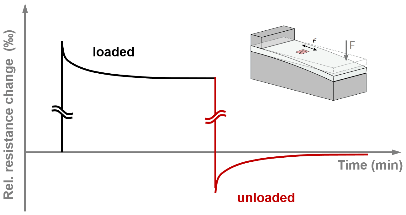
A Leybold Web-400SP web and foil sputtering system is used to produce thin films of about 100–150 nm thickness on various substrate materials and formats such as fused silica glass, silicon wafers, high-temperature resistant polyimide foils (PI foils), and transmission electron microscope (TEM) meshes. Some details of both the reactive sputtering process and the substrate materials are given in recently published papers (Mathis et al., 2021, 2020). The sputtering system has a cylindrical geometry with a big barrel onto which the substrates are mounted. The barrel is heated and is rotating underneath the target during the process time of approx. 1 h. All metal containing carbon films, considered in this study, are deposited by radio frequency sputtering of metal targets (dimension 400 mm×125 mm), with a focus on Ni, and NiCr alloys, but also NiW, NiV, and Pd are examined. The sputtering is performed in argon gas with a low addition of a carbon containing reactive gas C2H4 (ethylene) in the range of 2 %–3 %. The ethylene to argon flow ratio was adjusted differently for the diverse metal components to ensure temperature coefficients of resistance (TCRs) in the range of ±200 ppm K−1 while maintaining high gauge factors of the sensor films. Otherwise, the temperature-related resistance changes would dominate the creep and drift measurements to such an extent that no usable measurement would be obtained. Another important parameter for achieving high strain sensitivities is an elevated substrate temperature during deposition, which was set to 250 ∘C for all processes. After deposition, the thin films were patterned by means of an ultrafast pulsed Nd:YVO4 laser system (3D-Micromac) with a wavelength of 355 nm and a pulse duration of less than 15 ps. These patterns consist of resistance meanders in two perpendicular directions, referred to as longitudinal and transverse, typically between 0.5 to 1 kΩ. Such patterns on fused silica substrates ( mm) are investigated in a measuring system (Schultes et al., 2018) to obtain the mechano-electrical properties. In this report, only the longitudinal gauge factor is considered, which is referred to as the gauge factor for simplicity. A sample with the resistive structures is clamped on one end, as schematically shown in Fig. 1. Uniform strain may be generated by bending the sample onto a given metallic radius. With a radius of 1000 mm a strain of is obtained, well below the flexural strength of approx. for fused silica. The sample resistances are measured for the period of 30 min, first in the loaded and then in the unloaded state resulting in curves schematically plotted in Fig. 1. The procedure of unloading and loading is repeated 10 times at a specified temperature, mostly room temperature and 80 ∘C in this study. The bending test device is placed in an oven and fully automated to allow the simultaneous measurement of up to four samples. The repeated measurements of one specimen are plotted in the same diagram, one upon the other, each curve beginning just after the unloading or loading event. Thus, diagrams of the sort of Fig. 2 are obtained, where we plot the relative resistance change versus time. From these measurements we calculate the characteristic values for the respective film composition and annealing conditions, i.e., the gauge factor, TC-gauge factor, TCR, creep, and drift. Additional drift measurements of the electrical resistances over longer periods of time are performed in a tube furnace under atmospheric conditions, while thermal post-treatments (anneals) in various furnaces are also done in ambient air. Due to a large number of measurements as well as frequent verification measurements on known samples together with continuous improvements of the apparatus, the measurement uncertainties can be given as follows: gauge factor of ±0.5; TCR of ±2 ppm K−1; creep of ±1 ppm per 30 min; drift of ±0.2 ppm h−1.
Measurement on coated PI foils are carried out differently. The structuring is performed with the same laser, yielding thin film foil strain gauges (foil SGs). After a thermal treatment, these foil SGs may be glued onto a four-point bending device described in Schwebke et al. (2018b) to measure the gauge factor of films on PI foils at room temperature.
X-ray diffraction (XRD, Bruker D8 with Cu–Kα wavelength 1.5406 Å) under grazing incidence (0.5∘), and a TEM JEOL JEM-2100 LaB6 with 200 kV accelerating voltage are employed as methods of physical layer analytics. The TEM is equipped with a Gatan Orius SC1000 CCD camera with 1024×1024 pixels for image acquisition. Electron energy loss spectroscopy (EELS) and energy-filtered transmission electron microscopy (EFTEM) analysis were performed using a Gatan image filter (GIF 2002) and a Gatan slow-scan camera (Model 850). Elemental maps of carbon (K-edge), oxygen (K-edge), nickel (L-edge), and chromium (L-edge) were acquired by the three-window method (using pre-edge1, pre-edge2 and post-edge, acquisition time 10 s). To enable cross-sectional imaging, lamellae were prepared with an FEI Versa3D focused ion beam (FIB) by depositing platinum support layers beforehand. The lamellae are cleaned with a gallium ion beam and transferred to a TEM grid with a micromanipulator.
3.1 Influence of the chromium content of NixCr1−x-C films and influence of thermal post-treatment
Four different alloy targets of the composition Nix-Cr1−x with x=1; 0.9; 0.5; 0 (wt %, respectively) allow the preparation of corresponding Nix-Cr1−x-C coatings with well-adjusted carbon contents for low TCR values. The typical hydrogen content was determined once in advance with similar Ni–C specimens by nuclear physical methods to about 15 at. % (Koppert et al., 2012). The concentration of the elements Ni, Cr and C was determined by depth-resolved X-ray photoelectron spectroscopy (XPS) of a Ni90-Cr10-C layer to Ni 64 at. %, Cr 6 at. %, C 30 at. %. Thus, the overall composition is around of at. %, which can only be regarded as a guide value because of uncertainties due to process variations and determination.
At first, layers sputtered form a pure nickel target (x=1) are compared with films of an alloy with x=0.9, yielding films of Ni–C and Ni90-Cr10-C, respectively. The resistances of both film materials in their as-deposited (unannealed) state are measured in the described manner, with the results plotted in Fig. 2. The Ni–C film (Fig. 2a) displays a negative creep curve – negative because the sign is determined in the loaded state, −107 ppm being the average of 10 repetitive measurements of 30 min duration. Gauge factor, TCR (calculated between 80 and 30 ∘C) and drift are also derived from the measurements and displayed as values in the graph. With a gauge factor of 18.2 and an applied strain of a resistance change of occurs upon loading, subsequently creeping for (i.e., −107 ppm) in the period of 30 min at a temperature of 81 ∘C. This intrinsic aftereffect is hardly noticeable at room temperature, but the magnitude of creeping increases with temperature. An Arrhenius plot yields activation energies of 0.1–0.3 eV for a physical process that increases exponentially with temperature. In addition, further effects seem to have an influence on the temperature-dependent creep defects, which is why we have devoted an extra paper to this topic (Mathis et al., 2021).
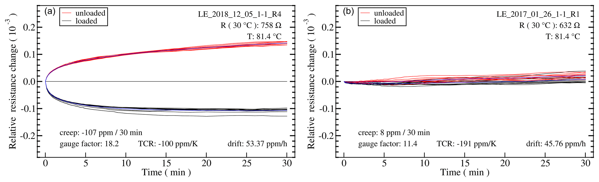
Figure 2Typical plot of a creep measurement with 10 repetitions at a temperature of about 81 ∘C. The relative change of resistance after the load change is plotted in parts per thousand on the ordinate. (a) Ni–C as-deposited (sample 1initial) (b) Ni90Cr10-C as-deposited (sample 2initial). From these measurements, characteristic values are calculated for the quantities: creep, gauge factor, TCR, and drift. These values are displayed in the graphs. During the time of the measurement (30 min), the resistance also changes due to drift, the value of which is given in the figures. As a result, the curves become asymmetric, since there is a superimposed drift to higher resistance values.
Films of Ni90-Cr10-C are strikingly different, because the creeping is reduced to only +8 ppm as shown in Fig. 2b. Another difference is the reduction of the gauge factor from 18 to a value of 11.
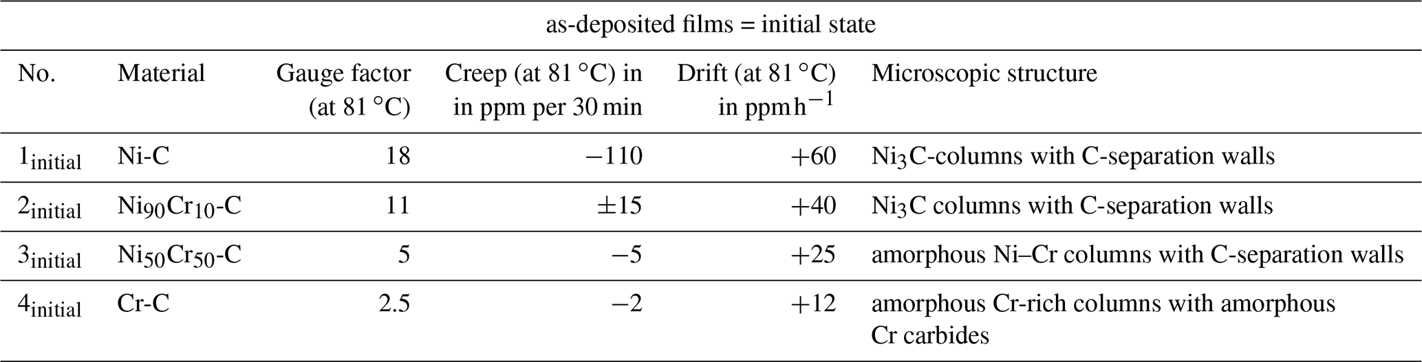
The four different NiCr targets, specified above, allow the determination of the characteristic sensor film parameters as given in Table 1. These values represent the state directly after sputtering (as-deposited), i.e., without further heat treatment; hence they are referred to as initial values. The data are averaged over a large number of depositions and measurements in order to show representative values unaffected by individual process variations. Replacing nickel with chromium obviously reduces both the strain sensitivity and the instabilities measured as creep and drift. Different microscopic structures are revealed in the physical analysis, which will be discussed further below. The most prominent structure features are noted in the last column of Table 1.
Table 1Initial mechano-electrical quantities of layers derived from the described measurements. These are the as-deposited or initial values without any post heat treatment. In the last column, some characteristic microscopic structural features of the layers are noted, which will be explained later.
The task is now to stabilize the films. Therefore, a lot of annealing processes under ambient air conditions were conducted with different temperatures and times. After these trials the measurements were repeated to extract the characteristic parameters. Not surprisingly, it turns out that different film materials require adapted heat treatments. It is possible to determine optimum annealing treatments, which lead to significantly lower values of creep and drift values as summarized in Table 2. This results in significantly more stable sensor films. In addition, the annealing slightly increases the sensitivity as represented by the gauge factors.
Table 2Final mechano-electrical quantities of the films after the thermal treatment in air, which is considered as optimal. The optimum annealing conditions in each case are given in the third column. In some cases, the microscopic structural features, which are again noted in the last column, are altered compared to the initial state.

With successive replacement of Ni by Cr, the thermal resistance (or thermal resilience) of the films increases. If pure Ni–C coatings can only be annealed at 225 ∘C without destroying the structure of columns and carbon separation walls, necessary for the high sensitivity, the optimum temperature for the Ni50Cr50-C composition is already 450 ∘C. Despite this high temperature, no continuous oxidation of the chromium-rich layers occurs, which would lead to a sharp increase in resistance and loss of measurement capability. Furthermore, the higher annealing temperatures apparently lead to very stable resistive layers. For example, the creep of the Ni50Cr50-C layer is lower by a factor of 10 than the already small value of the improved Ni90Cr10-C layer. The Ni50Cr50-C composition leads to the currently most stable sensor layer with an elevated gauge factor of 8. Only the Cr–C layer with a standard sensitivity of 2.5 has even better stability values. In the last column of Table 2, characteristic microscopic changes of the layer morphologies due to annealing are noted, which are obviously related to the described properties and will be discussed in the following.
3.2 How does the thermal post-treatment influence the microscopic structure of NixCr1−x-C films?
By means of FIB cross-section preparation and subsequent thinning, it is possible to image approx. 30–40 nm thin lamellae in the TEM. Due to the high contrast of the constituent elements C as well as Ni and Cr, high-contrast TEM images of the layers, which are deposited on PI foils and consolidated by Pt support layers, are obtained. All investigated layers exhibit the well-known columnar structure, of typically about 10 nm thin metal-rich columns in the growth direction separated by carbon walls (Abrasonis et al., 2009; Mel et al., 2012; Bayer et al., 2016; Schultes et al., 2018). No characteristic differences between layers of Ni–C and Ni90Cr10-C can be identified in TEM bright field, neither in the as-deposited state (samples 1initial and 2initial according to Table 1), nor in the finally annealed state (samples 1final and 2final according to Table 2). As an example of such a cross-section, a Ni90Cr10-C layer is shown in Fig. 3. The lattice plane spacing of d=0.23 nm in the growth direction of the columns (see Fig. 3b) is interpreted as nickel carbide Ni3C (110) (Uhlig et al., 2013). In this context, it should be noted that it is practically impossible to distinguish hexagonal close-packed (hcp) Ni, rhombohedral Ni3C, and hcp Ni3C because the three structures have almost identical lattice plane spacings (He, 2010; Uhlig et al., 2013).
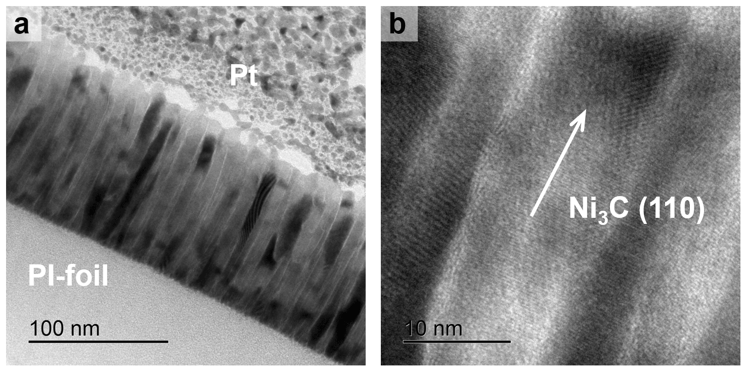
Figure 3Cross-section TEM bright field images of a layer of Ni90Cr10-C. (a) as-deposited (sample 2initial) (b) after heat treatment of 300 ∘C per 4 h (sample 2final) in high-resolution mode.
Our thorough TEM analysis does not reveal any structural differences between a Ni–C layer with a gauge factor of 18 and a chromium-containing Ni90Cr10-C layer with a gauge factor of 11. The XRD studies also show that both layers consist of nickel carbide Ni3C (or the indistinguishable hcp Ni). However, the peaks of Ni90Cr10-C films are always shifted to smaller 2θ values, i.e., to larger lattice spacings, compared to those of Ni–C. This suggests that Cr atoms partly replace Ni atoms, thereby widening the lattice. It is known that considerable amounts of chromium can be dissolved in the Ni-face centred cubic (fcc) lattice (Saltikov, 2003) as well as in the ternary system Ni–Cr–C (Velikanova et al., 1999). Thus, in the Ni3C system studied here, Ni is also replaced by Cr and the lattice is widened a little. In order to investigate the stability of Ni90Cr10-C films over a longer period of time, a long-term annealing of 8.5 d at a temperature of 240 ∘C, i.e., below the temperature of 300 ∘C, which is considered to be the optimum stabilization temperature for this material, was carried out. PI-foil pieces with Ni90Cr10-C films were removed from the furnace at the indicated times (see Fig. 4) and examined both by XRD and for their gauge factors by gluing the foil SG onto a four-point bending device. This investigation reveals a correlation between the strain sensitivity and the lattice plane spacing d101 of the Ni3C columns, measured at the 2θ position of the most intense XRD peak. A clear decrease and approach of the lattice plane spacing to the d101 literature value of 0.203 nm (He, 2010) is observed, accompanied by a concomitant increase of the gauge factor. From further measurements with these foil SGs, a re-increasing creep error is also measured. We interpret this relationship in such a way that chromium atoms escape from the column structure by diffusion, depleting it of chromium and returning it to a more or less pure Ni3C structure. As a result, the mechano-electrical properties associated with variant 1final are restored; i.e., the higher gauge factor and higher creep is returning. This long-term annealing below a certain stabilization temperature changes the originally more electrically stable chromium-containing column material and returns it back to the more unstable material with Ni–C properties.

Figure 4Evolution of the lattice plane spacing d101 and the gauge factor of Ni90Cr10-C layers annealed in air at 240 ∘C for a total duration of 8.5 d. (1) The gauge factors measured by four-point bending were converted to the values of the radius method and thus adjusted for the influence of transverse contraction. (2) The gauge factor in this series does not start at 11 (as in Table 1), but at about 9. This is attributed to slightly different coating parameters.
The question of why a chromium-containing material can nevertheless be permanently stabilized by annealing at an optimum temperature (according to Table 2) can be clarified with an element distribution study (EELS-EFTEM) carried out in the TEM on cross-section samples. Immediately after coating Ni90Cr10-C , i.e., in the as-deposited state, the elements Ni and Cr are equally distributed in the columns, while C is predominantly localized in the separation walls, as shown in the sequence of images in Fig. 5a. Optimum annealing (300 ∘C per 4 h) leaves the columns with graphite-like separation walls inside, while Cr diffuses to the outside boundaries, where it oxidizes to form a protective layer of chromium oxide (Fig. 5b). In this state, the sensor properties have an optimum, with a high gauge factor as well as low creep and drift values.
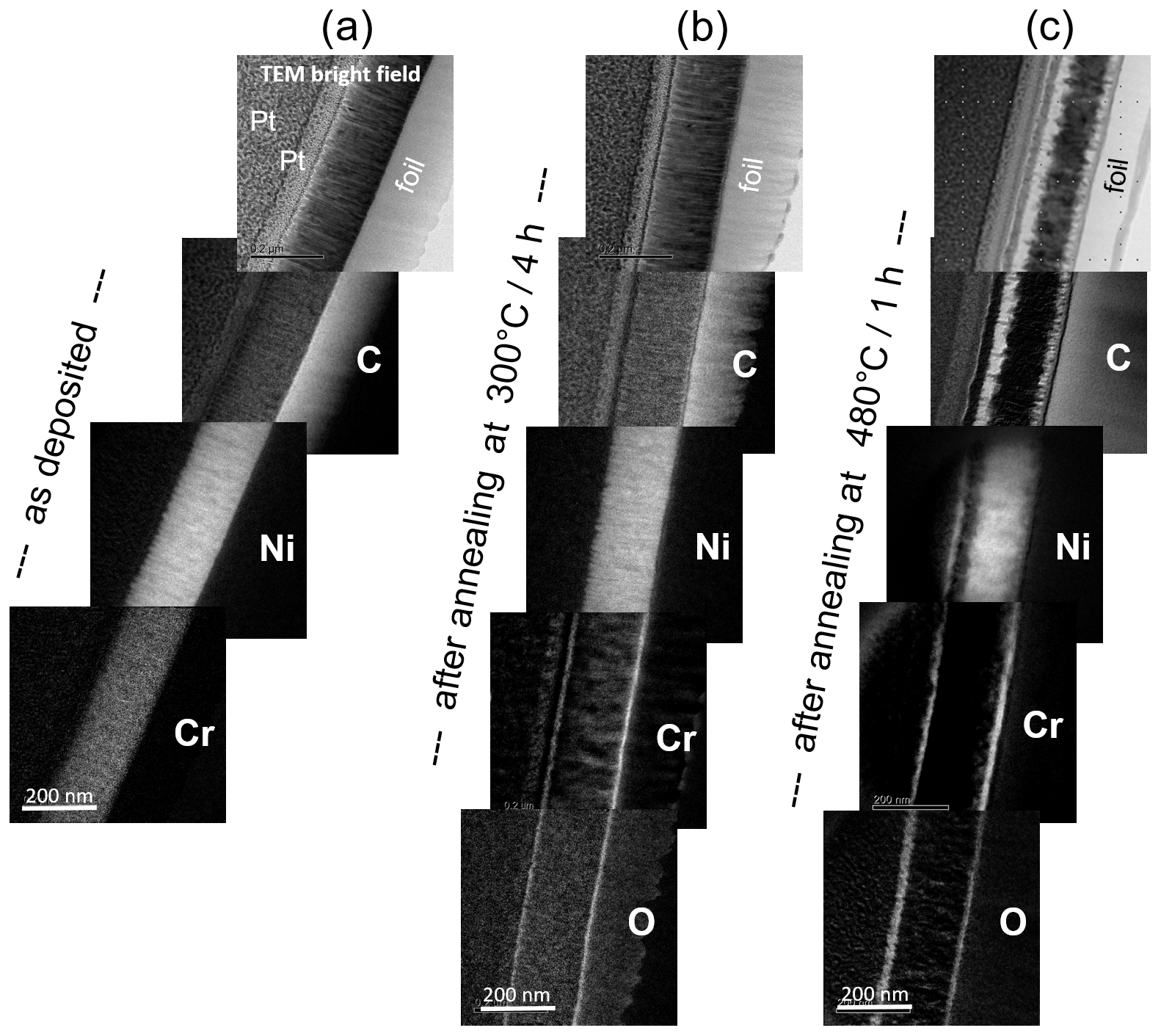
Figure 5Elemental distribution study (EELS-EFTEM) on layers of Ni90Cr10-C on PI foil. (a) as-deposited (b) after annealing at 300 ∘C per 4 h (c) after annealing at 480 ∘C per 1 h. The upper pictures of each row represent a bright field image of a cross-section of the layer. Below, the element maps of C, Ni, Cr, O are arranged so that the cross sections continue in a line. The indicated element signal is shown in white color and means that the element is present at these positions. The scale bars have a length of 200 nm.
If a much higher temperature is applied for annealing (480 ∘C per 1 h), additional segregation occurs (Fig. 5c) and the spatial distribution changes. Carbon is now also driven outward and a phase transformation of Ni3C to Ni-fcc (cubic phase of nickel) takes place inside. Now the layer consists of an inner zone of metallic nickel surrounded on both sides by carbon and terminated at the boundary on both sides by chromium-rich oxide sub-layers. Due to this segregation and transformation, the electrical properties of the complete layer are associated to a more or less metallic layer, and in fact, a purely metallic gauge factor of 2 and a positive TCR of about 1500 ppm K−1 are measured.
This makes it clear why optimum annealing results in a more stable sensor layer. Inside the film, the structure of the metal-containing columns with graphite-like separating walls is healed, while chromium oxide boundary layers simultaneously form protective layers. Whether such a chromium oxide layer also forms on the interface to the substrate depends on the oxygen permeability of the substrate material used. Polyimide film is permeable, while silicon or fused silica are not. Accordingly, a bottom chromium oxide layer forms on the substrate side of PI foil, but not on the other substrates. In any case, a chromium oxide layer is formed on the top free film surface. The results are described and summarized in the model sketches of Fig. 6.
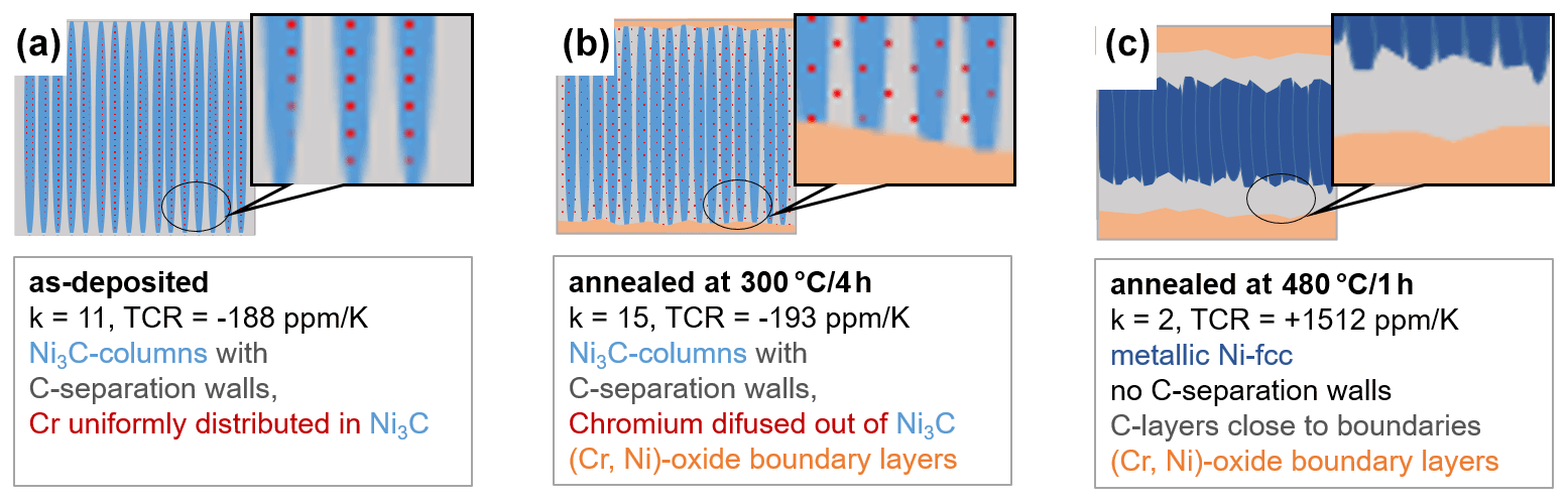
Figure 6Model sketches of Ni90Cr10-C films after different annealing treatments. (a) as-deposited (b) after annealing at 300 ∘C per 4 h (c) after annealing at 480 ∘C per 1 h. The electrical properties and structural microscopic features, derived from the TEM element distribution measurements, are noted in the boxes. Further explanations are given in the text.
An even better stabilization of the films is achieved by further increasing the chromium content, but at the expense of strain sensitivity. This is illustrated by the investigation of the Ni50Cr50-C material. After deposition, no crystalline fraction can be detected in this layer (sample 3initial). Only amorphous material is identified, both in XRD examination as well with TEM. However, a columnar structure of metal elements with intermediate regions of carbon is clearly visible in the TEM. In contrast to the previously described material, a double layer of chromium forms outside the column region already during deposition. This is attributed to the higher chromium content and outlined in the model sketch of Fig. 7a. After the subsequent, much higher optimum annealing temperature (350 ∘C per 5 h + 450 ∘C per 5 h), the material is not only still intact as a sensing layer, but is also extremely electrically stable (sample 3final). Annealing at such elevated temperatures causes various transformation and segregation processes, as sketched in Fig. 7b:
-
The columns crystallize to pure metallic Ni-fcc, the thermodynamically stable structure of nickel.
-
The carbon separation walls between the columns are preserved or become more pronounced.
-
Near-interface carbon layers form outside the columns, as already described for the lower chromium variant.
-
The film is again sealed on both sides by chromium oxide boundary sublayers.
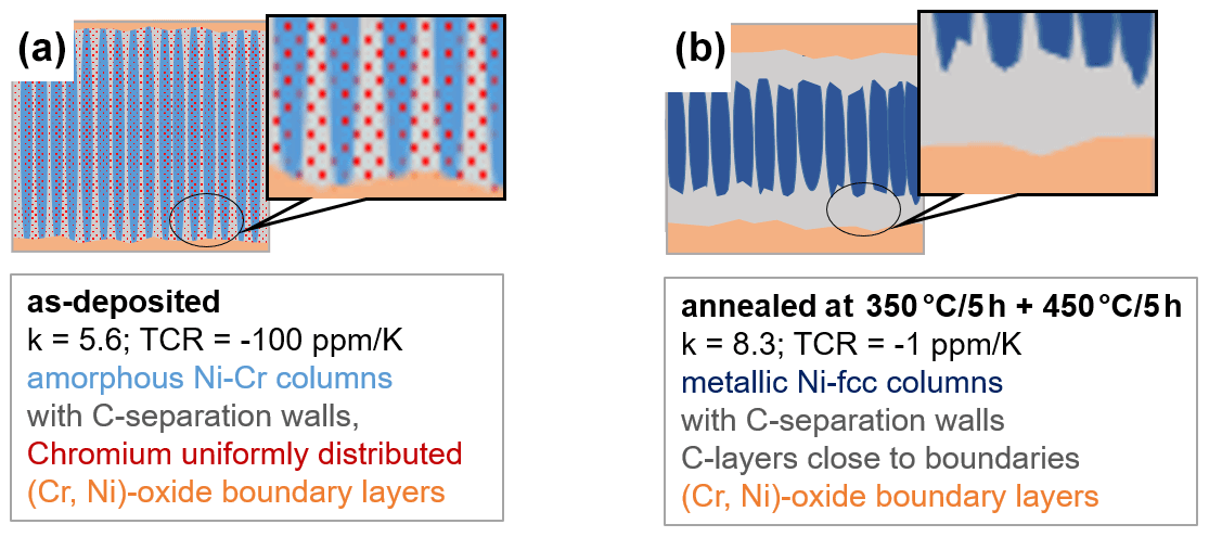
Figure 7Model sketches of films of Ni50Cr50-C. (a) as-deposited (b) after annealing at 350 ∘C per 5 h + 450 ∘C per 5 h. The electrical properties and structural microscopic features, derived from the TEM element distribution scans are noted.
The very high mechano-electrical stability of these films of Ni50Cr50-C annealed at 350 ∘C per 5 h + 450 ∘C per 5 h is manifested as follows. With a gauge factor of still 8, both creep and drift are lower than in any previously described variant with enhanced sensitivity (see sample 3final of Table 2). The success of this stabilization is visualized with measurements of the creep and drift parameters before and after the annealing process as shown in Fig. 8. Almost no disturbing instabilities remain.

Figure 8Creep measurements and drift values of Ni50Cr50-C films. (a) as-deposited (sample 3initial) (b) after annealing at 350 ∘C per 5 h + 450 ∘C per 5 h (sample 3final).
For the optimized Ni50Cr50-C strain gauges under the annealing conditions given in Table 2, we additionally performed a very long drift measurement (over 120 h) at the higher temperature of 125 ∘C (instead of 80 ∘C) in a tube furnace under atmospheric conditions. We obtained a resistance drift of only 0.3 ppm h−1, indicating exceptional stability. Such sensor layers could already be tested in an application for cylinder pressure sensors under harsh environmental conditions (Vollberg et al., 2022). The gauge factor is linearly dependent on strain as is also verified in this publication.
At this point we would like to draw attention to the nature of the chromium oxide compounds at the interfaces. Different oxides of chromium are known. Among them are CrO (chromium(II) oxide), which does not exist as bulk material but can be grown epitaxially as thin films on suitable monocrystalline substrates (Rogojanu et al., 2002); Cr2O3 (chromium(III) oxide), known as a very stable non-conducting passivation layer on stainless steel and also used as green pigments for corrosion protection; CrO2 (chromium(IV) oxide), which is electrically conductive and used as ferromagnetic tape emulsion; Cr2O5 (chromium(V) oxide), also conductive, being tested as cathode material for rechargeable batteries (Feng et al., 2016); and CrO3 (chromium(VI) oxide), a semiconducting toxic compound used in chrome plating. The question of which of the possible chromium oxide compounds are formed at the interfaces could be clarified with XRD measurements under grazing incidence. Unlike the expected Cr2O3, we could only find peaks of the very rare CrO compound, which are relatively clear to see. However, these peak positions coincide exactly with the nickel oxide NiO. Therefore, we cannot exclude the possibility that the interfaces consist of a mixture of CrO and NiO, which we named (Cr, Ni) oxides as marked in Table 2 and the Figs. 6 and 7. With higher and longer annealing we observed more and more difficulties to access the film resistance with low noise using measuring pins. Contact resistances indicate a non-conductive sublayer forming on the surface. By depositing an additional contact layer onto the pads, this difficulty could be overcome without affecting the sensor characteristics.
The series of investigations is completed by a Cr–C layer in which the entire nickel content is replaced by chromium. XPS analysis reveals a Cr content of 51.5 at. % and C of 47 at. % in the annealed layer. Chromium oxides can again be detected at the boundary interfaces, protecting the whole film. The corresponding resistivity of sample 4final (see Table 2) shows extremely good stability, at the complete expense of additional strain sensitivity with a gauge factors of 2.5, i.e., the almost purely geometrically determined metallic value.
3.3 Stabilization experiments with other elements
The stabilizing effect is probably due to the formation of dense chromium oxide boundary layers as shown in the results. The ability of chromium oxide to provide protection is known and for instance described for thin film strain gauges by Dyer et al. (1998). Therefore, coatings that do not have these protective layers should be significantly more unstable. To further support this argument, we introduced the elements tungsten and vanadium into the Ni–C sensor layer instead of chromium. However, the Ni85W15-C films prepared did not show a comparable good result, as the electrical parameters could not be sufficiently stabilized even though these films were annealed at 240 ∘C for 48 h. The gauge factor is about 14 in both the deposited and annealed state. In these layers, nickel-containing columnar structures separated by carbon walls can also be detected clearly. After annealing, a slight increase of the tungsten concentration at the surface is detected, but a lot of tungsten still rests in the inner layer. Thus, it is not possible to build up a dense protective oxide layers for electrical stabilization. The same holds true for the system nickel–vanadium (Ni93V7-C) that was also briefly tested. At last, instead of nickel–carbon, the system palladium–carbon, Pd–C was investigated. Beside Ni–C, Pd–C is the only alternative sensor film material with a significant enhancement of strain sensitivity as revealed in our previous study (Schultes et al., 2018). But in terms of stability Pd–C is very much different from the above discussed Ni–C. Layers of Pd–C show a very high drift already without mechanical load that could not be stabilized. So far, our investigations underline the necessity of adding chromium as a stabilizing element to Me–C sensor layers.
Columnar, highly strain-sensitive nickel–carbon films exhibit temporal instabilities, which are manifested by creep under load changes as well as by electrical drift of the resistor layers. Both phenomena increase with increasing measurement temperature. The investigations of this project clearly show how such sensor layers can be electrically stabilized. The increasing replacement of nickel by the element chromium causes a significant stabilization. The creep can be reduced to a rest of about 1 % and the drift to about 10 % of the initial values of Ni–C; the instabilities are thus hardly detectable in the stabilized systems. Thus, the so stabilized films are definitely usable for metrological precision applications. However, the increasingly improved electrical stability comes at the price of a loss of strain sensitivity, which drops to the pure geometrical value when nickel is completely replaced by chromium. A compromise while maintaining a sensitivity well above the standard value of 2 for coatings of Nix-Cr1−x-C is found in a range of x=0.5 to 0.9. Higher chromium contents allow the layers to be stabilized at higher annealing temperatures without destroying the columnar character of Ni3C with C separation walls and thus the cause of the elevated sensitivity. The stabilizing effect of chromium is revealed by microscopic physical analysis. The annealing process drives segregation processes in the layer material. While the layer interior is depleted of chromium and carbon, new boundary layers are formed. Carbon is located near the boundaries, while the layer is sealed off at the surface by chromium, which oxidizes in air and forms stable chromium oxide protective layers. High annealing temperatures heal the column structure of Ni3C or Ni-fcc and C separation walls inside, and the sensitivity increases accordingly. On the outside, chromium oxide boundary layers apparently form chemically very stable protective layers, which protect against further reactions and corrosion phenomena (Dyer, 1998). The formation of various chemical Cr–O bonds was also shown for non-hydrogenated nickel and chromium containing carbon films (Dovydaitis et al., 2021). This observed mechanism is reminiscent of the protective effect caused by the addition of chromium in the production of stainless steel (Hamada et al., 2010) and nickel-based alloys (Wang et al., 2021). Chromium forms a thin chromium oxide layer at the stainless steel surface if the Cr atoms are present in sufficient concentration and are not bonded as carbides. As is known, this increases the chemical and temperature resistance of steel.
In any case, the working hypothesis that slip and gliding processes in graphite-like carbon structures could lead to the observed resistance changes does not seem to be confirmed. Such slip or creep processes are known to occur in graphite-like materials when subjected to external forces and internal stresses. The assumption was that hard chromium carbides make it more difficult for the graphite-like planes, which form as C-separation layers around the nickel-containing columns, to move and slip, thus reducing the creep and drift values. However, since elemental distribution analysis proves that chromium migrates from the interior to the fringes, chromium carbide can hardly be present in the graphite-like separating walls. Instead, the protective boundary layers of chromium-rich oxides cause the electrical stabilization of the layers.
The question of which measures of layer preparation can eliminate the instabilities without reducing the strain sensitivity cannot be answered by the study, but the following direction can be deduced. High gauge factors are obtained in the low-chromium containing Ni–C material. The gauge factor can be further increased by more energy input during deposition, in the form of elevated substrate temperatures and substrate bias. On the other hand, chromium in the form of chromium oxide boundary layers is needed for stabilization. These two requirements could be separated by starting and ending the coating with a thin layer of chromium, but sputtering chromium-free Ni–C in between at the highest possible energy input. However, one of our past investigations has shown only low gauge factors with such a start layer of chromium. Another possibility is to continue working with Ni50Cr50-C material, sputtering it with more energy input to obtain a higher starting gauge factor and then annealing it as high as possible. At present, this appears to be the most promising option for achieving gauge factors >15 with excellent stability after a suitably high stabilization temperature.
Our analysis is useful for future applications in the field of pressure and force sensing, because our contribution allows us to show how metal-containing carbon layers need to be sputtered and thermally treated to obtain long-term stable sensor layers. For classical strain gauge-based transducers as well as for micro-electromechanical-system (MEMS) sensors, temperature-stable thin films properties are needed, which do not change during the long lifetime. The nickel- and chromium-containing carbon coatings described above are particularly suitable for this purpose because, in addition to their very stable resistance values, both their TCR and the temperature dependence of the gauge factor are adjustable and very low. These sensor layers stand alongside the likewise piezoresistive amorphous or diamond-like carbon coatings (Peiner et al., 2007) and a group of carbon-containing ceramic nanocomposites, such as those described in a recent review article (Ricohermoso et al., 2021). However, little is reported on their temperature dependencies of electrical resistance and it is feared that the putative high values cannot be compensated for, since no metal components are available for this purpose. Furthermore, to the authors' knowledge, the long-term stability of such films has not yet been reported.
This investigation clearly shows how highly strain-sensitive nickel-based carbon-containing sensor layers can be stabilized electrically. The partial replacement of nickel by chromium results in a significant stabilization. Creep and drift aftereffects can be reduced very effectively, but at the cost of strain sensitivity. A good compromise while maintaining sensitivities well above the standard value of 2 is identified for films with nickel : chromium ratios from 90 % : 10 % to 50 % : 50 %, stabilized by optimized temperature treatments. With more chromium the optimum annealing temperature is higher leading to better stabilization. The stabilizing effect of chromium is revealed by physical analysis. The annealing drives segregation processes in the coating material. While the interior of the layer is depleted of chromium and carbon, boundary sub-layers are formed. Carbon is enriched near the boundary, while the layer is sealed by chromium, which oxidizes in air and forms stable chromium oxide layers, which apparently represent chemically very stable protective layers against further reactions and corrosion like degradation.
By combining electrical sensor measurements with microscopic analysis methods such as electron microscopy and X-ray diffraction, the composition and structure of the thin films can be correlated with the electrical sensor properties. Thanks to the understanding of these structure-dependent sensor parameters, further improvements of sensor layers become possible. As a first result, the creep and drift errors have been greatly reduced. The optimized sensor coatings are now suitable for widespread use. The investigation shows how to eliminate the temporal aftereffects under load and temperature while maintaining a relative high sensitivity.
The underlying measurement data are not publicly available and can be requested from the authors if required.
All authors designed the experiments. MC performed and analyzed the depositions and the electrical measurements. AL performed the XRD measurements and MK the TEM specimen preparation and TEM analysis. All authors analyzed and discussed the results. GS wrote the manuscript with contributions of all authors. All authors approved the final version of the manuscript.
The contact author has declared that neither they nor their co-authors have any competing interests.
Publisher's note: Copernicus Publications remains neutral with regard to jurisdictional claims in published maps and institutional affiliations.
The authors kindly appreciate the support of all members of the Sensors and Thin Film Group at the htw saar – University of Applied Sciences.
This research has been supported by the Deutsche Forschungsgemeinschaft (grant nos. SCHU 1606/6-1 and KO 5371/1-1). The financial support is gratefully acknowledged.
This paper was edited by Bernhard Jakoby and reviewed by two anonymous referees.
Abrasonis, G., Kovacs, G. J., Ryves, L., Krause, M., Mücklich, A., Munnik, F., Oates, T. W. H., Bilek, M. M., and Möller, W.: blackboxPlease provide all authors abbreviated to last name comma initial(s).: Phase separation in carbon-nickel films during hyperthermal ion deposition, J. Appl. Phys., 105, 083518, https://doi.org/10.1063/1.3110187, 2009.
Bayer, B. C., Bosworth, D. A., Michaelis, F. B., Blume, R., Habler, G., Abart, R., Weatherup, R. S, Kidambi P. R., Baumberg, J. J., Knop-Gericke, A., Schloegl, R., Baehtz, C., Barber, Z., Meyer, J., and Hofmann, S.: In situ observations of phase transitions in metastable nickel (carbide)/carbon nanocomposites, J. Phys. Chem. C, 120, 22571–22584, 2016.
Cerino, M., Göttel, D., Probst, A. C., and Schultes, G.: Schichtwiderstand mit einem kohlenstoffhaltigen Widerstandsmaterial und Verfahren zu dessen Herstellung, Patent DE102015006057A1, 2015.
Dovydaitis, V., Marcinauskas, L., Ayala, P., Gnecco, E., Chimborazo, J., Zhairabany, H., and Zabels, R.: The influence of Cr and Ni doping on the microstructure of oxygen containing diamond-like carbon films, Vacuum, 191, 110351, https://doi.org/10.1016/j.vacuum.2021.110351, 2021.
Dyer, S. E., Gregory, O. J., and Cooke, J. D.: Improved passivating Cr2O3 scales for thin film high temperature PdCr strain gages, Thin Solid Films, 312, 331–340, 1998.
El Mel, A. A., Bouts, N., Grigore, E., Gautron, E., Granier, A., Angleraud, B., and Tessier, P. Y.: Shape control of nickel nanostructures incorporated in amorphous carbon films: From globular nanoparticles toward aligned nanowires, J. Appl. Phys., 111, 114309, https://doi.org/10.1063/1.4728164, 2012.
Feng, X. Y., Chien, P. H., Rose, A. M., Zheng, J., Hung, I., Gan, Z., and Hu, Y. Y.: Cr2O5 as new cathode for rechargeable sodium ion batteries, J. Solid State Chem., 242, 96–101, 2016.
Hamada, E., Yamada, K., Nagoshi, M., Makiishi, N., Sato, K., Ishii, T., Fukuda, K., Ishikawa, S., and Ujiro, T.: Direct imaging of native passive film on stainless steel by aberration corrected STEM, Corros. Sci., 52, 3851–3854, 2010.
He, L.: Hexagonal close-packed nickel or Ni3C?, J. Magn. Magn. Mater., 322, 1991–1993, 2010.
Heckmann, U., Bandorf, R., Petersen, M., Gwozdz, V., and Brauer, G.: Matching of maximum gauge factor and TCR zero crossing of Me–DLC, in: 2011 IEEE Sensors, Limerick, Ireland, 472–475, 28–31 October 2011, https://doi.org/10.1109/ICSENS.2011.6126973, 2011.
Jansson, U. and Lewin, E.: Sputter deposition of transition-metal carbide films – A critical review from a chemical perspective, Thin Solid Films, 536, 1–24, 2013.
Jiang, C. W., Ni, I. C., and Tzeng, S. D.: Nearly isotropic piezoresistive response due to charge detour conduction in nanoparticle thin films, Sci. Rep.-UK, 5, 11939, https://doi.org/10.1038/srep11939, 2015.
Karapepas, C., Nestler, D., Wett, D., and Wagner, G.: Annealing effects of high sensitive thin strain gauges consisting of nickel carbon nanocomposites, J. Reinf. Plast. Comp., 37, 1378–1384, 2018.
Koppert, R., Uhlig, S., Schmid-Engel, H., Göttel, D., Probst, A. C., Schultes, G., and Werner, U.: Structural and physical properties of highly piezoresistive nickel containing hydrogenated carbon thin films, Diam. Relat. Mater., 25, 50–58, 2012.
Mathis, M., Vollberg, D., Langosch, M., Göttel, D., Lellig, A., and Schultes, G.: Novel method to reduce the transverse sensitivity of granular thin film strain gauges by modification of strain transfer, J. Sens. Sens. Syst., 9, 219–226, https://doi.org/10.5194/jsss-9-219-2020, 2020.
Mathis, M., Vollberg, D., Langosch, M., Göttel, D., Lellig, A., and Schultes, G.: Creep adjustment of strain gauges based on granular NiCr-carbon thin films, J. Sens. Sens. Syst., 10, 53–61, https://doi.org/10.5194/jsss-10-53-2021, 2021.
Peiner, E., Tibrewala, A., Bandorf, R., Lüthje, H., Doering, L., and Limmer, W.: Diamond-like carbon for MEMS, J. Micromech. Microeng., 17, S83, 2007.
Petersen, M., Bandorf, R., Bräuer, G., and Klages, C.-P.: Diamond-like carbon films as piezoresistors in highly sensitive force sensors, Diam. Relat. Mater., 26, 50–54, https://doi.org/10.1016/j.diamond.2012.04.004, 2012.
Ricohermoso III, E., Rosenburg, F., Klug, F., Nicoloso, N., Schlaak, H. F., Riedel, R., and Ionescu, E.: Piezoresistive carbon-containing ceramic nanocomposites – a review, Open Ceramics, 5, 100057, https://doi.org/10.1016/j.oceram.2021.100057, 2021.
Rogojanu, O. C., Sawatzky, G. A., and Tjeng, L. H.: Stabilizing CrO by epitaxial growth, Doctor of Philosophy, Groningen, https://research.rug.nl/files/3045848/thesis.pdf (last access: 25 February 2022), 2002.
Saltikov, P.: Hochtemperatur-Thermochemie im System Al-Cr-Ni-O, Dissertation, Universität Stuttgart, https://doi.org/10.18419/opus-6521, 2003.
Schultes, G., Frey, P., Goettel, D., and Freitag-Weber, O.: Strain sensitivity of nickel-containing amorphous hydrogenated carbon () thin films prepared by rf sputtering using substrate bias conditions, Diam. Relat. Mater., 15, 80–89, 2006.
Schultes, G., Schmid-Engel, H., Schwebke, S., and Werner, U.: Granular metal–carbon nanocomposites as piezoresistive sensor films – Part 1: Experimental results and morphology, J. Sens. Sens. Syst., 7, 1–11, https://doi.org/10.5194/jsss-7-1-2018, 2018.
Schwebke, S., Werner, U., and Schultes, G.: Granular metal–carbon nanocomposites as piezoresistive sensor films – Part 2: Modeling longitudinal and transverse strain sensitivity, J. Sens. Sens. Syst., 7, 69–78, https://doi.org/10.5194/jsss-7-69-2018, 2018a.
Schwebke, S., Winter, S., Koch, M., and Schultes, G.: Piezoresistive granular metal thin films of platinum–boron nitride and platinum–alumina at higher strain levels, J. Appl. Phys., 124, 235308, https://doi.org/10.1063/1.5054972, 2018b.
Tamulevičius, S., Meškinis, Š., Tamulevičius, T., and Rubahn, H. G.: Diamond like carbon nanocomposites with embedded metallic nanoparticles, Rep. Prog. Phys., 81, 024501, https://doi.org/10.1088/1361-6633/aa966f, 2018.
Uhlig, S., Struis, R., Schmid-Engel, H., Bock, J., Probst, A. C., Freitag-Weber, O., and Schultes, G.: Piezoresistive thin films containing hcp-Ni or Ni3C investigated by XRD, EXAFS, and wavelet analysis, Diam. Relat. Mater., 34, 25–35, 2013.
Velikanova, T. Y., Bondar, A. A., and Grytsiv, A. V.: The chromium-nickel-carbon (Cr-Ni-C) phase diagram, J. Phase Equilib., 20, 125, 1999.
Vollberg, D., Gibson, P., Schultes, G., Groh, H.-W., and Heinze, T.: Smart in-cylinder pressure sensor for closed-loop combustion control, J. Sens. Sens. Syst., 11, 1–13, https://doi.org/10.5194/jsss-11-1-2022, 2022.
Wang, Z., Carrière, C., Seyeux, A., Zanna, S., Mercier, D., and Marcus, P.: XPS and ToF-SIMS Investigation of Native Oxides and Passive Films Formed on Nickel Alloys Containing Chromium and Molybdenum, J. Electrochem. Soc., 168, 041503, https://doi.org/10.1149/1945-7111/abf308, 2021.