the Creative Commons Attribution 4.0 License.
the Creative Commons Attribution 4.0 License.
 | 12 Apr 2023
Compact silicon-based attenuated total reflection (ATR) sensor module for liquid analysis
Armin Lambrecht
Carsten Bolwien
Hendrik Fuhr
Gerd Sulz
Annett Isserstedt-Trinke
André Magi
Steffen Biermann
Jürgen Wöllenstein
Infrared attenuated total reflection (ATR) spectroscopy is a common laboratory technique for the analysis of highly absorbing liquids and solids, and a variety of ATR accessories for laboratory FTIR spectrometers are available. However, ATR spectroscopy is rarely found in industrial processes, where compact, robust, and cost-effective sensors for continuous operation are required. Here, narrowband photometers are more appropriate than FTIR instruments. We show the concept and implementation of a compact Si-based ATR module with a four-channel microelectromechanical systems (MEMS) detector. Measurements of liquid mixtures demonstrate the suitability for applications in the chemical industry. Apart from sapphire (for wavelengths below 5 µm) and diamond (extending to the far-infrared region), most materials for ATR elements do not have either high enough infrared transmission or sufficient mechanical and chemical stability to be exposed to process fluids, abrasive components, or aggressive cleaning agents. However, using diamond coatings on Si improves the stability of the sensor surface. In addition, by proper choice of incidence angle and coating thickness, an enhancement of the ATR absorbance is theoretically expected and demonstrated by first experiments using a compact sensor module with a diamond-coated Si ATR element.
- Article
(2470 KB) - Full-text XML
- BibTeX
- EndNote


Infrared attenuated total reflection (ATR) spectroscopy is a common technique for the analysis of highly absorbing liquid or solid samples. When radiation in an optical material is totally reflected at an interface with a material of a lower index of refraction, part of the wave penetrates into the sample. The penetration depth of this evanescent wave, i.e., the probed sample thickness, is approximately equal to the radiation wavelength λs in the sample (Harrick, 1965, 1987). In the mid-infrared (MIR) range ( µm), this corresponds to only a few micrometers. In the laboratory, ATR has widespread applications, e.g., in medical diagnostics (Heise et al., 2001; Lambrecht et al., 2006), food quality analysis (Su and Sun, 2019), the beverage industry (Anton Paar, 2022; Centec, 2022), water contamination monitoring (Lu et al., 2013), determination of moisture in transformer and lubrication oil (Sim and Jeffrey Kimura, 2019), pharmaceutical process analytics (Helmdach et al., 2013), and monitoring of rubber polymerization (Dubé and Li, 2010).
Most materials for MIR ATR spectroscopy do not have either high enough infrared transmission or sufficient mechanical and chemical stability to be exposed to process fluids, abrasive components, or aggressive cleaning agents. Up to a wavelength of 5 µm, sapphire is a suitable and established material (Anton Paar, 2022; Centec, 2022; Lambrecht et al., 2020). For longer wavelengths, diamond is the usual choice. However, because of the high costs, only very small diamond elements, e.g., tiny crystals at the tip of fiber probes, are generally employed (art photonics GmbH, 2022; IFS GmbH, 2023). These diamond crystals only allow a few ATR reflections, so the sensitivity is reduced compared to planar sensors with larger ATR elements. However, rugged probes with a planar diamond crystal allowing multiple ATR reflections are also available and have been successfully used for process analytics in a laboratory environment (Koch et al., 2015; Steinbach et al., 2020; Gasser et al., 2018).
ATR crystals, e.g., Si, Ge, and ZnSe, may be used for the longer-wavelength MIR range. But these materials are not sufficiently robust for use in industrial processes to be exposed to process fluids, abrasive components, and aggressive cleaning-in-place (CIP) agents (Pike Technologies, Inc., 2022). For applications in, e.g., chemical and food industries, sensors have to withstand mechanical scrubbing, hot water vapor, and acids and bases.
In previous work (Arndt et al., 2021), we have investigated nanocrystalline diamond (NCD) coatings on Si ATR elements. With these coatings, a sufficient robustness of the ATR elements against CIP agents was observed. In general, one would expect a reduction in the sensitivity of a coated ATR element compared to an uncoated crystal. However, theoretical and experimental results indicate that by a proper choice of angle of incidence, coating thickness, and wavelength, an enhancement of the absorbance can be achieved. These results are outlined in Sect. 2.
Compared to a laboratory, industrial processes require compact, robust, and cost-effective sensors for continuous operation. Here, narrowband photometers are more appropriate than FTIR instruments. Harnessing microelectromechanical systems (MEMS) technologies and packaging techniques already established for infrared detectors and emitters, a compact sensor device can be realized. A concept of a miniaturized and highly integrated MEMS ATR sensor based on Si wafer processing was proposed and investigated by de Graaf et al. (2008). However, this concept has only a limited radiation throughput, which is too low for sensitive ATR measurements. In Sect. 3 we describe a hybrid packaging concept which enables the incorporation of state-of-the-art MEMS thermal emitters and optimized thermopile detectors. Based on this concept, we fabricated two compact ATR sensors with Si-ATR elements, one uncoated and one protected with an NCD coating.
In Sect. 4 we report first measurements with these sensors using solutions of acetonitrile (AC) and of the BASF product Basonat HI100 (trimerized hexamethylene diisocyanate (HDI)) in propylene carbonate (PC), which we have used previously (Lambrecht et al., 2020; Arndt et al., 2021). Isocyanates are important base chemicals for many applications. We observe for the first time an enhancement of the sensitivity by an NCD coating in a compact Si-based ATR sensor. Finally, we discuss the results and give an outlook.1
If radiation is internally reflected at an interface of two materials with refractive indices n1 and n2 (n1>n2), the wave is totally reflected at the interface if the angle of incidence α is higher than the critical angle αc. It is defined as follows, where n1 and n2 are the real parts of the refractive indices of ATR crystal and sample, respectively.
Within the ATR crystal with refractive index n1, a standing wave is formed, and because of the boundary conditions, the electromagnetic field decays exponentially into the sample. This field is called the evanescent field.
The penetration depth of the evanescent wave is in the range of the wavelength (λ) in the sample. The wavelength-dependent absorption of the evanescent wave leads to an attenuation of the reflected beam. By measuring the spectral dependence of the reflected beam intensity, an ATR spectrum is obtained. In analogy to transmission spectroscopy, this is expressed by the absorbance A:
where R describes the polarization-dependent reflection factor which can be calculated using the Fresnel equations (Milosevic, 2012). A is dimensionless. However, in spectroscopy, absorbance units (denoted AU) and milli-absorbance units (denoted mAU) are commonly used. Throughout this paper, we use this convention.
Figure 1a shows the theoretically calculated, angle-dependent absorbances for different ATR crystal materials and water at the strong absorption band at 3.03 µm. If an ATR element with multiple reflections is used, the absorbance increases proportionally to the number of reflections.
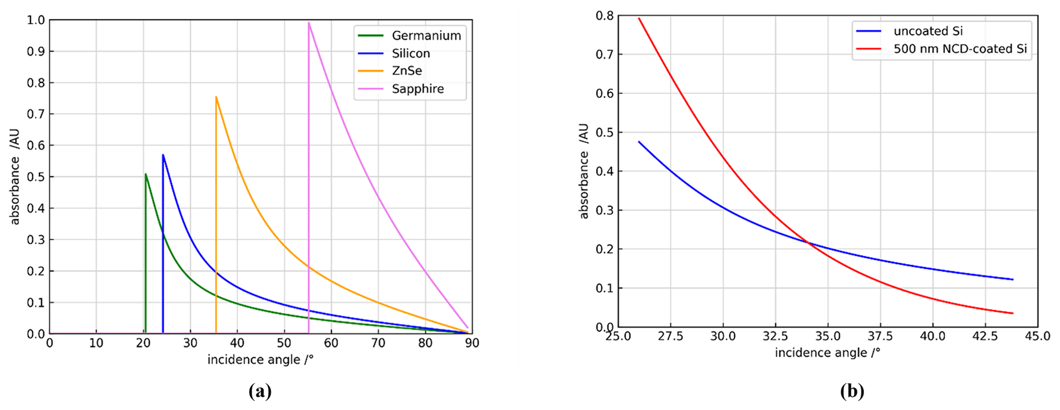
Figure 1(a) Theoretical absorbance of water at 3.03 µm for the ATR materials germanium, silicon, zinc selenide, and sapphire. (b) Dependence of the water absorbance at 3.03 µm on the angle of incidence for uncoated Si and NCD-coated Si with a thickness of 500 nm. Calculations according to Arndt et al. (2021).
In Arndt et al. (2021) the theory was extended for coated ATR crystals and applied to the special case of Si ATR elements coated by a film of nanocrystalline diamond (NCD). It was shown that the ATR effect is strongly influenced by the covering layer. The coating leads to an amplification by a factor of absorbancecoated / absorbanceuncoated for angles smaller than 33∘ (Fig. 1b). As the angles increase, the decrease in the absorbance of the coated system is stronger than for the uncoated element. Experiments using uncoated and NCD-coated Si hemispheres qualitatively confirmed the theoretical results. Further details, e.g., the influence of the coating thickness and spectral dependence of the amplification, can be found in the given reference.
The basic idea for a compact and cost-effective ATR sensor is to harness established packaging technologies such as MEMS infrared detectors and emitters. Similar to infrared windows for detectors, the ATR element may be soldered into the cap of a hermetically sealed housing which contains the radiation source and the infrared detectors and some electronics.
A concept of a miniaturized and highly integrated MEMS ATR sensor was previously proposed and investigated (de Graaf et al., 2008). However, this concept has only a limited radiation throughput, which is too low for sensitive ATR measurements. Here, we used a hybrid packaging concept which enables the incorporation of state-of-the-art MEMS thermal emitters and thermopile detectors.
An important component of the sensor is the ATR element. In a first step we decided to use Si with its readily established packaging technologies. However, the surface of the Si element facing the process media has to be coated to withstand mechanical wear and aggressive chemical cleaning agents. In a second step, this approach may be extended to similar materials like Ge, also with appropriate coating.
3.1 Preparation and characterization of nanocrystalline diamond films on silicon
Silicon ATR elements (37.5 mm × 10 mm × 1.5 mm) were obtained from Korth Kristalle GmbH, Altenholz, Germany. Several samples were coated with nanocrystalline diamond (NCD) films using a hot filament chemical vapor deposition (HFCVD) process at GFD GmbH, Ulm, Germany. Typical HFCVD process parameters at GFD GmbH, Ulm, Germany. Typical HFCVD process parameters using CH4 and H2 as main reaction gases were substrate temperatures of 750 to 900 ∘C, filament temperatures of 1900 to 2200 ∘C, chamber pressures between 1 and 20 mbar, and growth rates of 50 to 400 nm h−1. Further details on the HFCVD process can be found in the literature, e.g., in Wang et al. (2004).
For process applications, the coating on a Si ATR surface must not have any defects. For that reason, exemplary tests were performed by GFD GmbH: visually defect-free NCD-coated Si samples were exposed to concentrated KOH, which is an established etching solution for Si. After rinsing and drying, the NCD coating was removed by an O2 plasma etching process. The formerly coated Si surface was then inspected for the occurrence of any etch pits by optical and scanning electron beam microscopy. In the case of pinholes in the NCD coating, such etch pits at the interface would have been formed by KOH intrusion. However, for NCD films with a thickness greater than 300 nm, no etch pits were observed, indicating that the original NCD coating was free of pinholes. Additionally, the suitability of NCD-coated Si elements for applications in the beverage industry was investigated by CENTEC GmbH, Maintal, Germany. Uncoated and NCD-coated Si elements were exposed to 5 % NaOH solutions at 80 ∘C for 200 h, 3 % HNO3 solutions at 40 ∘C for 200 h, a soft drink (cola) at 15 ∘C for 400 h, and beer at 5 ∘C for 400 h. Additionally, the samples were exposed to hot water at temperatures up to 100 ∘C for 100 h. Subsequent visual inspection showed that the coated sides of the samples were not affected by the agents. FTIR transmission spectra taken before and after the treatment of the coated samples did not show a difference. In comparison, uncoated Si surfaces were not stable.
3.2 Optical concept and simulation
The original idea of the project was to use established Si wafer processing for the ATR module. To obtain the wedged crystal face for coupling (in and out) of the infrared radiation, an anisotropic etching process was planned (see Fig. 2a). In subsequent steps, one side of the wafer would be coated by a diamond film, followed by metallization of joints; finally, by dicing of the wafer, the elements are obtained, ready for assembly. By anisotropic etching, a wedge angle of β=54.74∘ is obtained.
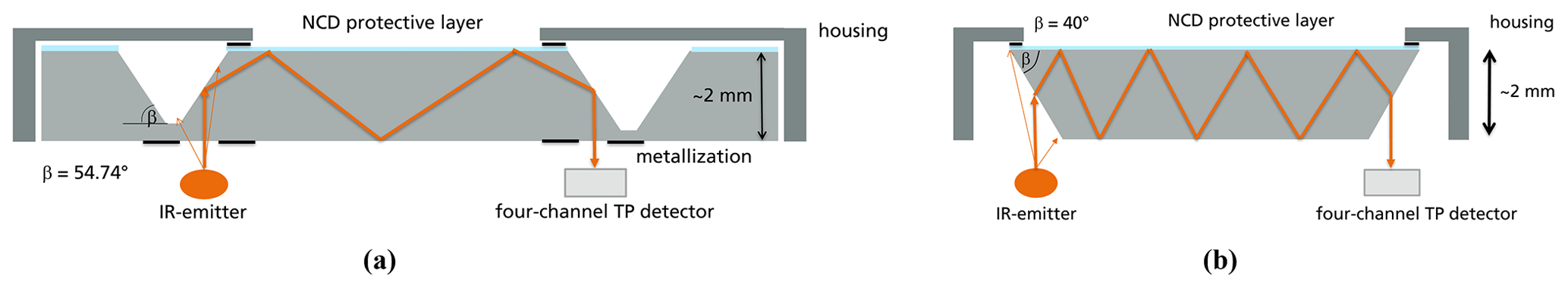
The radiation of a thermal emitter impinges perpendicularly from below. After a series of reflections, the radiation exits again perpendicularly at the bottom of the ATR element. For the IR source, an array of four individual thermal emitters was chosen to fully illuminate the ATR element and the linear detector array which consists of four thermopile detectors with individually selected narrowband pass filters.
However, a closer look at the optics shows that only large angles of incidence at the sample face, far off the critical angle of Si (see Fig. 1a) and far off a possible angle for an expected amplification by a diamond coating according to Sect. 2, can be achieved by this concept. With β=54.74∘, an angle of incidence α=70.52∘ is obtained. As shown in Arndt et al. (2021), this would result in a considerable attenuation of the absorbance compared to an uncoated Si ATR element. In contrast, amplification of the absorbance would require a wedge angle β≥73.5∘, which makes in-coupling of thermal radiation very difficult for ATR crystals with a thickness of less than 2 mm.
Thus, we decided to take mechanically cut and polished Si crystals with a wedge angle of β=40∘ and use those in an inverse geometry (Fig. 2b). For Si, this would yield an angle of incidence at the sample face of α=30∘, theoretically resulting in a significant amplification by a diamond coating of suitable thickness. Furthermore, this configuration would also be fitting for Ge crystals with 40∘ wedges, resulting in a 31∘ angle of incidence.
With these Si crystals, nominally 22 ATR reflections and a corresponding high sensitivity are expected. Practically, this is considerably reduced by the divergence of the radiation source. However, it demonstrates the high gain in sensitivity which could be achieved by using high-index ATR materials, compared to, for example, sapphire.
The setup in Fig. 2b still has the advantage of perpendicular optical radiation coupling from below. Substantial reflection losses at the in-coupling face are expected for high refractive index materials such as Si and Ge if no antireflection coating is used. However, for unpolarized thermal radiation sources usually employed in ATR sensors, the total reflectances for 0 and 40∘ incidence angles at the air–Si interface are equal and have a value of 30 %.
Both configurations in Fig. 2a and b were investigated using the ray tracing simulation software Zemax OpticStudio 16 (Zemax Europe, Ltd., Essex, UK). The simulation clearly proved the advantages of the concept in Fig. 2b for ATR elements of Si and Ge.
3.3 Concepts for sensor electronics and packaging
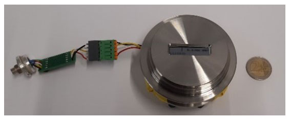
The ATR sensor consists of a hermetically sealed ATR sensor module with thermal emitters, detectors, and two electronics boards adapted to it. In Fig. 3a an exploded schematic view of the ATR sensor module is shown.

Figure 3(a) Exploded schematic view of the ATR sensor module assembly. (b) Side view of the sensor with both electronics driver boards connected to the hermetically tight ATR sensor module.
In the elongated package, the ATR crystal is soldered directly into the housing lid. This cover is later laser-welded onto the housing base. These two joining technologies guarantee a hermetic, long-term, stable seal and therefore increase the stability of the system with demanding environmental requirements. To raise the radiation power, an emitter array consisting of four elements is provided. The overlying beam stop prevents stray radiation in the housing. At the radiation exit face of the ATR crystal, a line array of four thermopiles with specific infrared narrow-bandpass filters (see Table 1) is positioned.
Table 1Spectral filters in front of the thermopile detectors: center wavelength, full width at half maximum (FWHM), and corresponding application.

For temperature compensation, a thermistor is provided, which is placed near the detectors. All components are located on low-temperature cofired ceramics (LTCC) wiring carrier, which is designed for thermopiles with a specific preamplifier stage for each of the four measurement channels. The housing offers the possibility to control the inner atmosphere by backfilling it with inert gas or setting a pre-vacuum. To increase the sensitivity of the thermopile chips, the package is backfilled via a copper tube with an inert gas having a low thermal conductivity. By using krypton, a sensitivity gain by a factor of 1.7 is achieved. After the gas-filling process, the copper tube is sealed hermetically by squeeze cold welding and a soldering process.
For the measurements two ATR modules were manufactured: one with an uncoated Si crystal and one Si crystal with a 500 nm NCD coating.
In order to integrate and adapt the circuit board to the size of the module, a two-part concept was chosen (Fig. 3b). The first printed circuit board was designed as a pure analog electronics board which contains all amplifiers for the analog signals. On this board, the ATR module is connected directly via a special 72-pin socket. As a result, it is possible to check different modules with one electronics board. On the second printed circuit board, the digital functions, the emitter driver stages, and the microprocessor are placed. Via a serial interface, the module can be parameterized, and measured values are transmitted. It is possible to read out the sensor signals with a high time resolution and to process them on a personal computer. Furthermore, the amplification of the voltage signals and the emitter power can be adjusted.
The detector module can be integrated into a Varivent flange (Fig. 4), which is frequently used in the beverage industry. A possible sensor application is the determination of the dissolved CO2 concentrations in beverages.
Apart from applications in the beverage industry, another promising application of the sensor is concentration determination of isocyanate solutions. Isocyanates are the base chemicals of polyurethane materials and are produced in high volumes worldwide. As in previous work (Lambrecht et al., 2020; Arndt et al., 2021), we used a solution of the BASF product Basonat HI100 (trimerized hexamethylene diisocyanate, HDI) in propylene carbonate (PC) as an example for an isocyanate solution. Later experiments were performed with solutions of acetonitrile (AC) in propylene carbonate (PC) as an alternative to the toxic isocyanates with similar spectroscopic properties. Even for CO2 quantification in the beverage industry, AC in PC (denoted ACPC) is a good model system and much easier to handle than pressurized dissolved CO2. Acetonitrile has a strong absorption at 4.44 µm.
All measurements were performed at room temperature. The signals of the four thermopile detectors were continuously recorded at a measurement interval of 2 s. The sample was alternated between air (A), solvent (PC), and the sample liquid (Basonat in PC and AC in PC, respectively). The absorbance A was evaluated according to
4.1 Sensor module with an uncoated Si ATR element
In a first experiment, a 1 % solution of Basonat (BA) in PC (denoted BAPC) was used as a sample (Fig. 5). The concentration changes between pure solvent and sample are clearly visible. For the PC steps, only a small drift is observed. However, the absorbance values for the air measurements (marked as A in the figure) show some variations. Probably, the cleaning of the sensor surface is difficult for the sticky BA solution. From the steps, the individual average absorbance values APC and AACPC, the corresponding change in absorbance Δ, the standard deviations σPC and σACPC, and the corresponding Allan deviations for 1 min integration time σAllan(1 min) are determined and listed in Table 2. For the calculation, the third PC step and the third BAPC step are used. As a result, Basonat concentrations in PC can be measured down to 100 ppm with the sensor module.
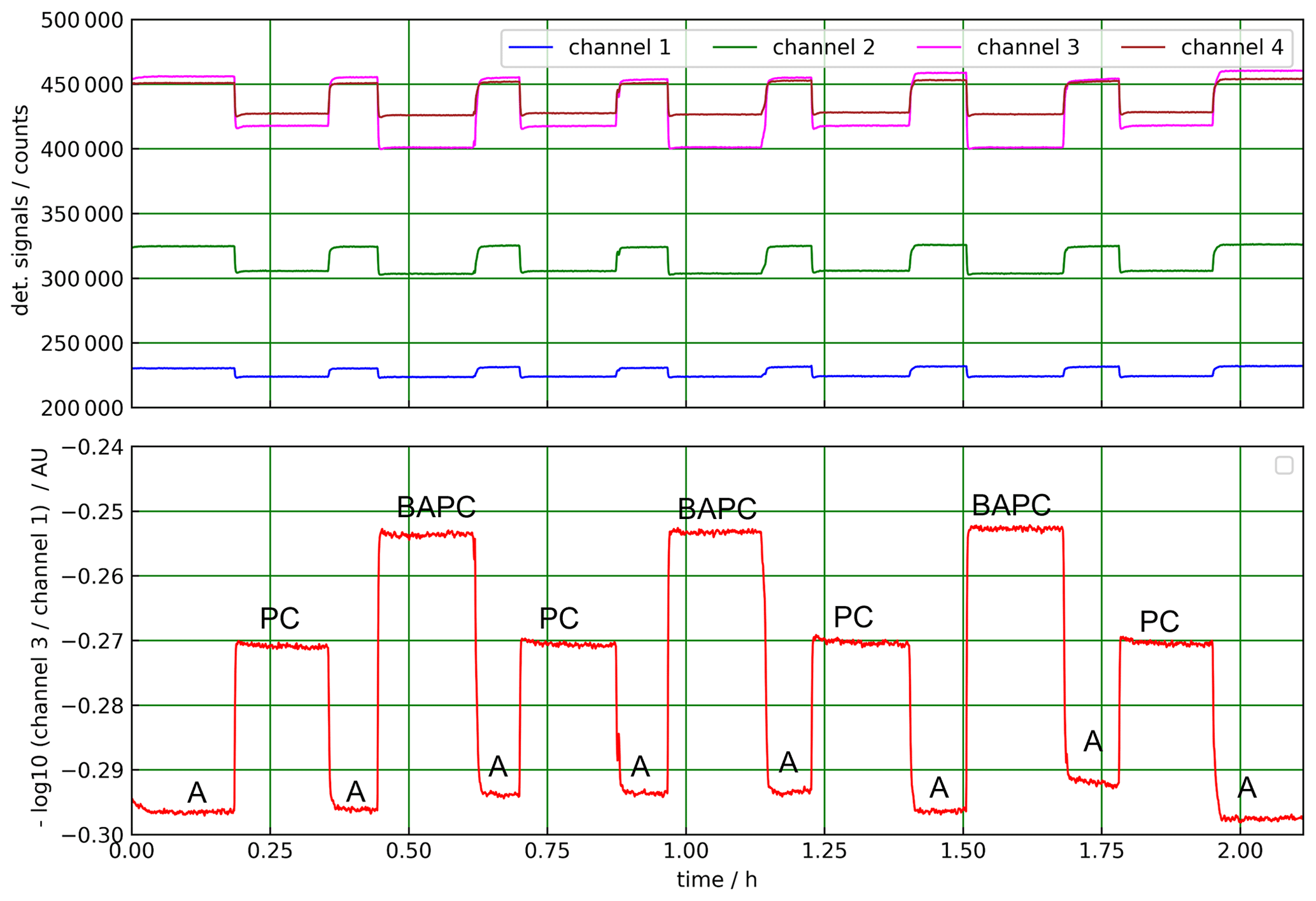
Figure 5ATR measurement with an uncoated Si ATR element. The ATR surface was alternately covered with solvent (PC) and a 1 % solution of Basonat in PC (BAPC). After each step, the surface was cleaned, and a measurement with ambient air (A) was performed.
Table 2Performance results of ATR measurements with uncoated and NCD-coated ATR elements.
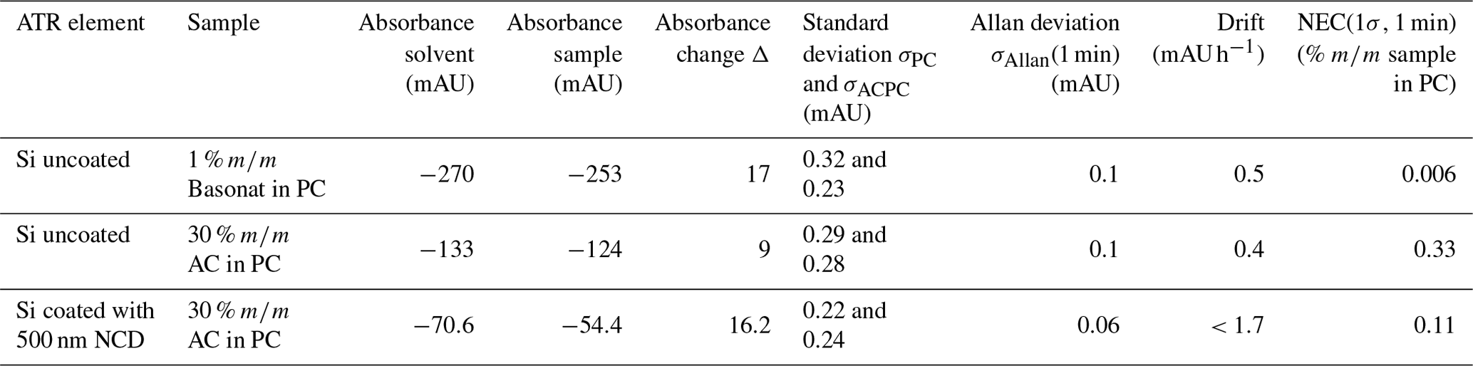
The next experiment was performed with PC as a solvent and a 30 % solution of AC in PC (Fig. 6). The steps caused by the sample changes are well reproduced over the total measurement duration of more than 2 h. The intermittent air value (marked as A) is reproducible as well and ensures proper cleaning of the ATR surface in contrast to Fig. 5. The data from Fig. 6 are listed in Table 2. For the calculations, the third PC step and the second ACPC step are selected. An estimation of the drift is also included. The low signal drift enables an integration time of 1 min. From the data, a noise equivalent concentration NEC(1σ,1 min) is obtained, demonstrating the measurement of AC concentrations in PC below 1 % with the sensor module.
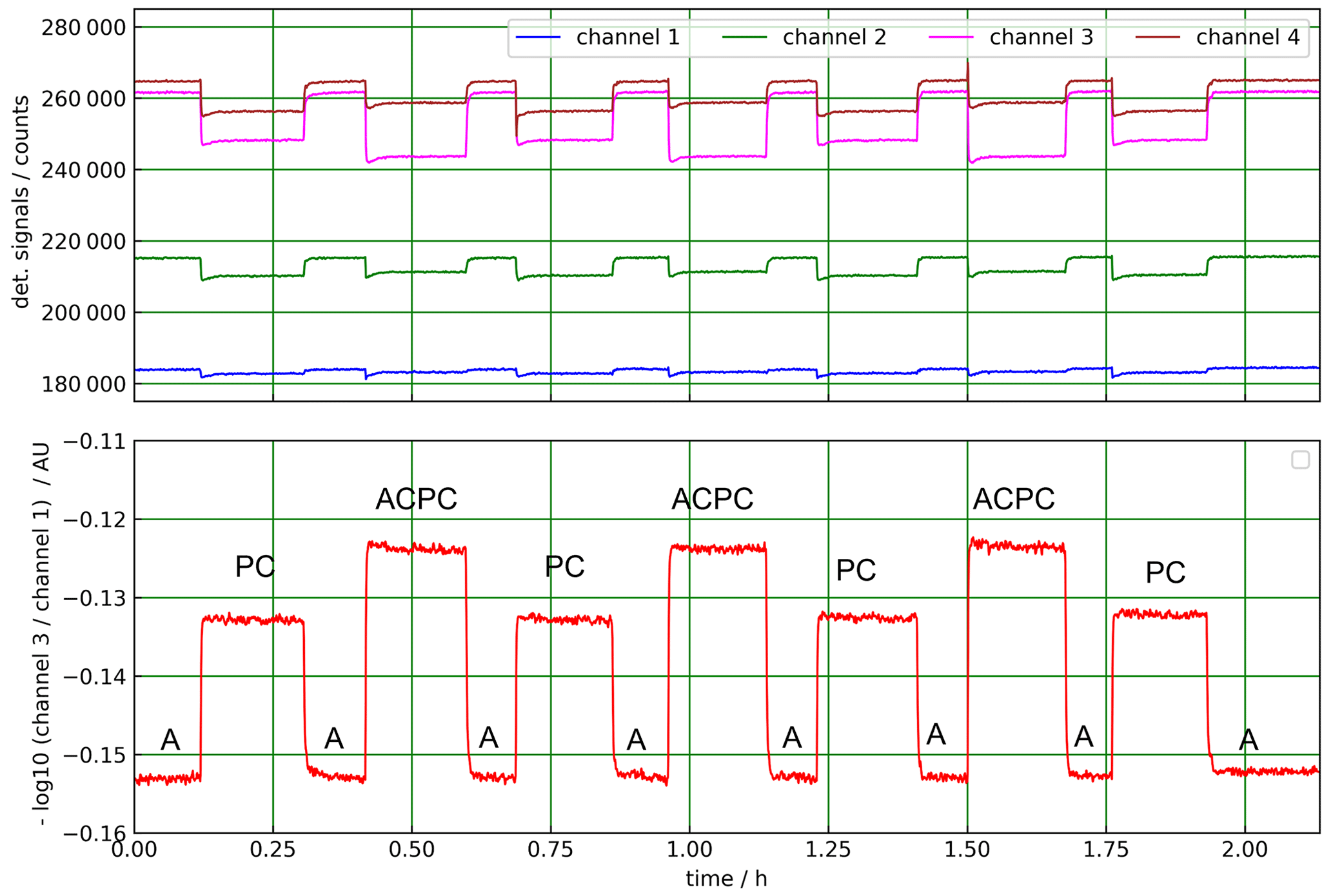
Figure 6ATR measurement with an uncoated Si ATR element. The ATR surface was alternately covered with solvent (PC) and a 30 % solution of AC in PC (ACPC). After each step, the surface was cleaned, and a measurement with ambient air (A) was performed.
4.2 Sensor modules with an NCD-coated Si ATR element
The third measurement was performed using a sensor module with an NCD-coated ATR element (see Fig. 7). The resulting data are also listed in Table 2. For the calculations, the fifth PC step and the fourth ACPC step are selected, which last longer than the previous steps. The measurement in Fig. 7 shows a stronger and slowly decreasing signal drift compared to Fig. 6. This might be caused by an initial temperature difference between the sensor and the sample liquids, which is less pronounced in the measurements in Fig. 6.
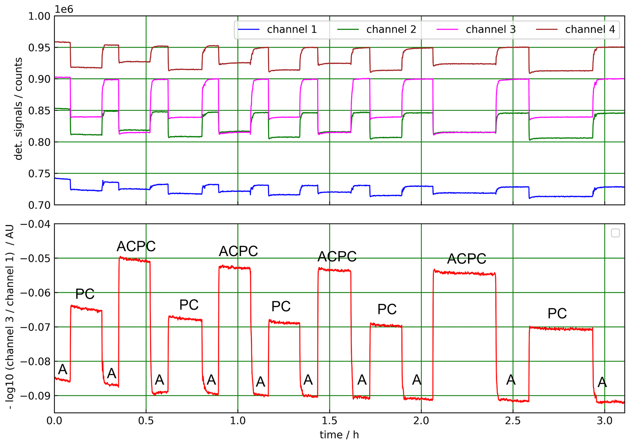
Figure 7ATR measurement using a Si ATR element coated with 500 nm NCD. The ATR surface was alternately covered with solvent (PC) and a 30 % solution of AC in PC (ACPC). After each step, the surface was cleaned, and a measurement with ambient air (A) was performed.
However, the main result of this measurement is an increased absorbance change for the sensor with the NCD-coated ATR element. The absorbance change is increased by a factor of 1.8 compared to the sensor with an uncoated Si element. Additionally, the absorbance noise is reduced for the coated element. Both factors add up to an increase in the signal-to-noise ratio (SNR) of the sensor along with a reduced NEC by a factor of 3 for the coated device.
The NEC values in Table 2 can be compared with previous photometric measurements (Lambrecht et al., 2020; Theuer et al., 2015). There, for BA in PC, an NEC(1σ,1 min) of 91 ppm () was determined using a sapphire ATR element. Our result in Table 2 agrees fairly well with this value. A further increase in the sensitivity for BA in PC is expected for diamond-coated Si ATR elements. From the data in Table 2, an NEC of 20 ppm () can be estimated. Hence, Si-based compact ATR sensors seem to be well suited for the determination of isocyanate concentrations at 100 ppm and above.
Furthermore, the measurement of BA in PC in Fig. 5 demonstrates the importance of cleaning. Obviously, residuals of a previous measurement were not always completely removed between the steps. For an ATR process sensor, complete and reproducible cleaning is essential, and the ATR surface has to withstand the required mechanical and chemical cleaning processes. This could be achieved by diamond coating. For automatic sensor operation and cleaning processes, additional condition monitoring of the ATR surface would be useful to ensure reliable operation.
The main result of this work is the experimental observation of an absorbance enhancement by a factor of 1.8 for an NCD-coated Si element compared to an uncoated Si crystal in a compact ATR sensor module. Recently, variable angle spectroscopy measurements with a 390 nm NCD-coated Si hemisphere and water at 3.03 µm have shown an enhancement factor of 1.4 for an incidence angle of 30∘ (Arndt et al., 2021). Compared to this value and to the theoretical value of 1.4 (from Fig. 1b), the observed enhancement factor is too large.
However, when results from two different sensor devices are compared, some uncertainties cannot be avoided. For example, the relative positions of light sources, detectors, and ATR elements may vary due to assembling tolerances. The angle of incidence and beam divergence may slightly differ from one device to the other. Our packaging concept (see Sect. 3) enables efficient and reproducible manufacturing of ATR sensors in similar quantities as MEMS infrared detectors. Hence, we expect a more accurate experimental determination of the enhancement factor when more devices and measurements are available.
To summarize, a compact Si-based ATR sensor module for liquid concentration measurements was developed. Similar to infrared detectors, the module housing is hermetically sealed. Processing and packaging steps are well established, and production could be rapidly scaled up to a substantial volume. Diamond-coated Si ATR elements are resistant against mechanical and chemical cleaning agents. For solutions of the isocyanate Basonat in propylene carbonate, a sensitivity of 100 ppm () is achieved. With coated Si ATR elements, an absorbance enhancement of 1.8 and a reduction of the NEC by a factor of 3 were observed compared to uncoated Si elements. Additionally, with Si the spectral range of the sensor is greatly enhanced in comparison to sapphire. Hence, more applications can be addressed by merely selecting other filters than those chosen in Table 1.
Generally, thermal and mechanical constraints of such compact modules do not allow inline use in demanding process applications. Some of these restrictions can be overcome by modifications without sacrificing the compact and cost-effective package. But there are many other applications left for such ATR sensors, which are currently performed with process FTIR spectrometers, e.g., quality control of lubricating oil (Wagner, 2023) or milk analysis (Foss, 2023). The compact sensor modules can be applied for fast at-line analysis and may also be incorporated into handheld instruments for fast and effective quality control of, for example, delivered raw materials.
Diamond-like carbon (DLC) coatings could be an alternative to the NCD films on Si ATR crystals (Suasnavas et al., 2019). DLC is an established protective coating for Ge infrared optics. DLC-coated Ge ATR elements will offer a broader spectral range and access to the MIR fingerprint range, which is important for selective sensor applications.
The underlying measurement data may be requested from the authors if required.
Conceptualization: GS, CB, SB; sensor design, packaging concept, and sensor assembly: AIT, AM, SB; optical simulation: CB, GS; measurements: HF; methodology: GS, CB, AL; data analysis: CB, AL; writing: AL; critical reading and revision of the manuscript: JW.
The contact author has declared that none of the authors has any competing interests.
Publisher's note: Copernicus Publications remains neutral with regard to jurisdictional claims in published maps and institutional affiliations.
This article is part of the special issue “Sensors and Measurement Systems 2022”. It is a result of the “Sensoren und Messsysteme 2022, 21. ITG/GMA-Fachtagung”, Nuremberg, Germany, 10–11 May 2022.
We gratefully acknowledge the support of our project partners GFD GmbH for supplying the NCD coatings and characterization and CENTEC GmbH for investigations on the chemical resistance of the NCD coatings on Si in cleaning agents.
This research has been supported by the Bundesministerium für Bildung und Forschung (BMBF) (grant no. FKZ 13N14577).
This paper was edited by Bernhard Jakoby and reviewed by two anonymous referees.
Anton Paar: Carbo 520 Optical, https://www.anton-paar.com/us-en/products/details/carbo-520-optical/, last access: 26 July 2022.
Arndt, N., Bolwien, C., Sulz, G., Kühnemann, F., and Lambrecht, A.: Diamond-Coated Silicon ATR Elements for Process Analytics, Sensors, 21, 6442, https://doi.org/10.3390/s21196442, 2021.
art photonics GmbH: Fiber Optic ATR-Probes, https://artphotonics.com/product/fiber-optic-atr-probes/, last access: 26 July 2022.
Centec: CARBOTEC NIR, https://www.centec.de/sensors/electronics-semiconductor/carbotec-nir/, last access: 26 July 2022.
de Graaf, G., der Vlist, W., and Wolffenbuttel, R. F.: Design and fabrication steps for a MEMS-based infrared spectrometer using evanescent wave sensing, Sensor. Actuat. A-Phys., 142, 211–216, https://doi.org/10.1016/j.sna.2007.09.009, 2008.
Dubé, M. A. and Li, L.: In-Line Monitoring of SBR Emulsion Polymerization Using ATR-FTIR Spectroscopy, Polym.-Plast. Technol., 49, 648–656, https://doi.org/10.1080/03602551003664909, 2010.
Foss: MilkoScan™ FT3, https://www.fossanalytics.com/en/products/milkoscan-ft3#Brochures_and_Papers, last access: 11 April 2023.
Gasser, C., Kilgus, J., Harasek, M., Lendl, B., and Brandstetter, M.: Enhanced mid-infrared multi-bounce ATR spectroscopy for online detection of hydrogen peroxide using a supercontinuum laser, Opt. Express, 26, 12169–12179, https://doi.org/10.1364/OE.26.012169, 2018.
Harrick, N. J.: Electric Field Strengths at Totally Reflecting Interfaces, J. Opt. Soc. Am., 55, 851–857, https://doi.org/10.1364/JOSA.55.000851, 1965.
Harrick, N. J.: Internal reflection spectroscopy, 3rd Edn., Harrick Scientific Corporation, Ossining, NY, 327 pp., ISBN 0-933946-13-9, 1987.
Heise, H. M., Voigt, G., Lampen, P., Kupper, L., Rudloff, S., and Werner, G.: Multivariate Calibration for the Determination of Analytes in Urine Using Mid-Infrared Attenuated Total Reflection Spectroscopy, Appl. Spectrosc., 55, 434–443, https://doi.org/10.1366/0003702011951948, 2001.
Helmdach, L., Feth, M. P., Minnich, C., and Ulrich, J.: Application of ATR-MIR spectroscopy in the pilot plant-Scope and limitations using the example of Paracetamol crystallizations, Chemical Engineering and Processing: Process Intensification, 70, 184–197, https://doi.org/10.1016/j.cep.2013.04.003, 2013.
IFS GmbH: MIR Fiber Probes with Diamond ATR FTIR Technology, https://ifs-aachen.de/, last access: 11 April 2023.
Isserstedt-Trinke, A., Lambrecht, A., Bolwien, C., Fuhr, H., Sulz, G., Magi, A., Biermann, S., and Wöllenstein, J.: Kompaktes ATR Sensormodul für die Flüssigkeitsanalyse, in: Sensoren und Messsysteme: Beiträge der 21. ITG/GMA-Fachtagung 10.–11. Mai 2022, Nürnberg, edited by: Reindl, L. M. and Wöllenstein, J., VDE VERLAG GmbH, Berlin, Offenbach, 275–276, ISBN 978-3-8007-5835-7, 2022.
Koch, C., Brandstetter, M., Wechselberger, P., Lorantfy, B., Plata, M. R., Radel, S., Herwig, C., and Lendl, B.: Ultrasound-Enhanced Attenuated Total Reflection Mid-infrared Spectroscopy In-Line Probe: Acquisition of Cell Spectra in a Bioreactor, Anal. Chem., 87, 2314–2320, https://doi.org/10.1021/ac504126v, 2015.
Lambrecht, A., Beyer, T., Hebestreit, K., Mischler, R., and Petrich, W.: Continuous glucose monitoring by means of fiber-based, mid-infrared laser spectroscopy, Appl. Spectrosc., 60, 729–736, 2006.
Lambrecht, A., Bolwien, C., Erb, J., Fuhr, H., and Sulz, G.: Cylindrical IR-ATR Sensors for Process Analytics, Sensors, 20, 2917, https://doi.org/10.3390/s20102917, 2020.
Lu, R., Mizaikoff, B., Li, W.-W., Qian, C., Katzir, A., Raichlin, Y., Sheng, G.-P., and Yu, H.-Q.: Determination of Chlorinated Hydrocarbons in Water Using Highly Sensitive Mid-Infrared Sensor Technology, Sci. Rep.-UK, 3, 2525, https://doi.org/10.1038/srep02525, 2013.
Milosevic, M.: Internal reflection and ATR spectroscopy, Chemical analysis, in: vol. 176, Wiley, Hoboken, NJ, 239 pp., ISBN 978-0-470-27832-1, 2012.
Pike Technologies, Inc.: Crystal Selection for ATR, https://www.piketech.com/atr-crystal-selection/, last access: 26 July 2022.
Sim, S. F. and Jeffrey Kimura, A. L.: Partial Least Squares (PLS) Integrated Fourier Transform Infrared (FTIR) Approach for Prediction of Moisture in Transformer Oil and Lubricating Oil, J. Spectrosc., 2019, 5916506, https://doi.org/10.1155/2019/5916506, 2019.
Steinbach, J. C., Schneider, M., Hauler, O., Lorenz, G., Rebner, K., and Kandelbauer, A.: A Process Analytical Concept for In-Line FTIR Monitoring of Polysiloxane Formation, Polymers, 12, 2473, https://doi.org/10.3390/polym12112473, 2020.
Su, W.-H. and Sun, D.-W.: Mid-infrared (MIR) Spectroscopy for Quality Analysis of Liquid Foods, Food Eng. Rev., 11, 142–158, https://doi.org/10.1007/s12393-019-09191-2, 2019.
Suasnavas, C. V., Makeev, M. O., Osipkov, A. S., Solano, N. B., Shupenev, A. E., and Mikhalev, P. A.: Relationship between hardness and optical properties of diamond-like carbon coatings, IOP Conf. Ser.-Mat. Sci., 675, 12051, https://doi.org/10.1088/1757-899X/675/1/012051, 2019.
Theuer, M., Hennig, S., Ferstl, W., Konz, W., and Lambrecht, A.: ATR photometer for the detection of isocyanate concentrations in process applications, tm - Technisches Messen, 82, 16–23, https://doi.org/10.1515/teme-2014-0036, 2015.
Wagner, C.: Used-oil Analysis Using a Portable FTIR Spectrometer, https://www.petro-online.com/article/analytical-instrumentation/11/eralytics-gmbh/used-oil-analysis-usingnbspa-portable-ftir-spectrometer/1728, last access: 11 April 2023.
Wang, T., Xin, H. W., Zhang, Z. M., Dai, Y. B., and Shen, H. S.: The fabrication of nanocrystalline diamond films using hot filament CVD, Diam. Relat. Mater., 13, 6–13, https://doi.org/10.1016/j.diamond.2003.08.014, 2004.
Part of our work is also shortly described in a recent German conference contribution (Isserstedt-Trinke et al. 2022).