the Creative Commons Attribution 4.0 License.
the Creative Commons Attribution 4.0 License.
 | 25 Aug 2023
Analysis of thermal-offset drift of a high-resolution current probe using a planar Hall resistance sensor
NamYoung Lee
Jaesoo Kim
DaeSung Lee
We developed a pin-type current probe with high sensitivity, targeting electrical-probing printed circuit boards (PCBs). The developed sensor showed good enough characteristics, with 1 mA resolution on current measurements and up to 1 MHz operating frequency for analyzing highly integrated PCBs. During its characterization, however, we experienced a monotonously varying output signal in the time range of a few tens of minutes. We modeled it as the thermal-offset drift, being caused by Joule heating during sensor operation, and showed several solutions for reducing the offset by modifying the planar Hall resistance (PHR) layout and electric operation conditions and applying sensor circuitry with pulse width modulation.
- Article
(2723 KB) - Full-text XML
- BibTeX
- EndNote


For various applications in modern medical, industrial, and home appliances and in smart mobile devices with high functionality and miniaturized features, high-spec integrated-circuit (IC) chips such as application-specific integrated circuits (ASICs) and digital signal processors (DSPs) are integrated into a high-end printed circuit board (PCB) with a sub-millimeter fine pitch. As the complexity and precision of electronic circuits increase, accurate measurement technology becomes more critical.
Multi-meters, oscilloscopes, spectrum analyzers, etc. are generally used to measure the real-time voltage waveform and frequency component and to analyze the circuit characteristics or failure mode by touching the voltage probe to the measurement point during the operation of the electronic circuits. However, detecting voltage fluctuations through signal measurements can be difficult in many cases with circuit defects. For example, there may be instances where voltage fluctuations caused by defects are absorbed or mitigated by impedance components such as capacitors or inductors in the surrounding circuit. Additionally, it can be challenging to detect defects through voltage waveforms in situations such as minute disconnections in the signal line or when floating occurs within the circuit.
Therefore, other metrologies like X-ray transmission (Ueda et al., 2021; Roh et al., 2003), infrared imaging (Zhang et al., 2014; Huang and Wu, 2010), or eddy current measurement (Koggalage et al., 2005; Chomsuwan et al., 2007) have been additionally applied for the analysis. However, these kinds of methods also have limits for overall analyses because they are partially helpful for finding some physical defects such as disconnections or shorts. Fundamentally, current waveform measurement during the operation of electronic devices needs to be analyzed for fast and efficient troubleshooting.
Currently, however, most commercialized current sensors can measure the current flow only when a signal line is inserted into a clamp-shaped probe. To monitor the current waveform of the line on the PCB using this sensor, it needs to disconnect the PCB pattern and re-connect with wires to insert them into the clamp. Unlike a voltage probe, this inevitably damages the PCB and is inconvenient for measuring multiple points. Therefore, developing a probe-type current sensor capable of measuring currents in real time by simply contacting or bringing the probe into close contact with the measurement point without damaging the PCBs is required. Although some probe-type current sensors have recently been released, with probe tip sizes of a few millimeters and a minimum current resolution of about 10 mA, they are still not satisfactory for analyzing high-end PCBs with sub-millimeter fine pitch sizes.
In this paper, we present the development of a pin-type current probe featuring a high-sensitivity magnetic-field sensor. The probe was designed to measure the current waveform of high-end printed circuit boards (PCBs) with sub-millimeter fine pitch at a minimum resolution of less than 1 mA (Fig. 1). The magnetic sensor applied here could be manufactured with a smaller size than several hundred micrometers using a thin-film PHR (planar Hall resistance) with high magnetic resolution of less than 0.01 µT, and a low-noise PHR-to-volt converter was developed. We will report the electric characteristics of the prototype samples.
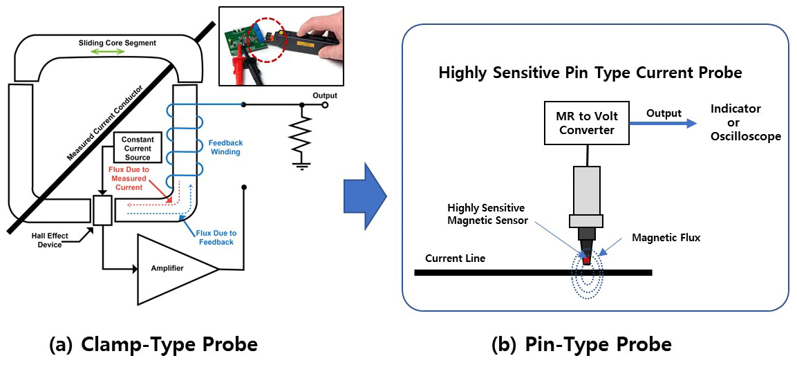
Figure 1Comparison of the two types of current probes. (a) Clamp-type probe – to measure the current, it needs to create a wire by modifying the PCB line and inserting it into the clamp. Inserted photograph from the Keysight website (https://www.keysight.com/kr/ko/lib/resources/selection-guides/oscilloscope-probes.html, last access: 21 August 2023). (b) Pin-type probe – the current is measured by directly sensing the magnetic field from a line of PCBs by simply bringing the probe into contact with the point.
2.1 Design of the PHR magnetic-field sensor
2.1.1 The principles of the PHR magnetic-field sensor
The PHR magnetic sensor uses the asymmetric magneto-resistance (AMR) material, whose resistivity has a different value depending on whether the current direction is parallel or perpendicular to the magnetization direction. The resistance of the magneto-resistive body varies depending on the angle between its magnetization and the current direction. When the magnetization rotates from the current direction, an electric-field component perpendicular to the direction is generated, and planar Hall voltage can be measured in the direction perpendicular to the current (Hansen and Rizzi, 2017).
In this study, the PHR structure, which is composed of NiFe–Cu–IrMn triple layers, was used to form the magneto-resistance material (Elzwawy et al., 2019; Sinha et al., 2013), and the PHR signal was enhanced by arranging the four PHR resistors in the form of a Wheatstone bridge. The initial magnetization is formed in the lower direction in Fig. 2, which is called the easy axis. The four resistors are arranged so that the current flows at the angle of ±45∘ to the easy axis, and the output signal becomes zero due to the symmetry of the Wheatstone bridge in the absence of an external magnetic field. When the direction of magnetization is rotated under the influence of an external magnetic field, however, a mismatch occurs between the four resistors due to the AMR effect, and the output signal proportional to the external magnetic field is generated.
If the four resistors in the Wheatstone bridge are ideally identical, there is no offset of the output signal (signal between B and D in Fig. 2 – VB−D) in the absence of a magnetic signal. However, if a mismatch between four resistors occurs due to loading effects in the manufacturing process, such as exposure, etching, or thin-film deposition, or if the easy axis (direction of initial magnetization Mo) is distorted in the direction of the horizontal axis, output signal offset may occur. Although the circuit function can remove the output offset itself, it can cause a thermal-offset drift due to Joule heating in the sensor operation mode (refer to Sect. 4).
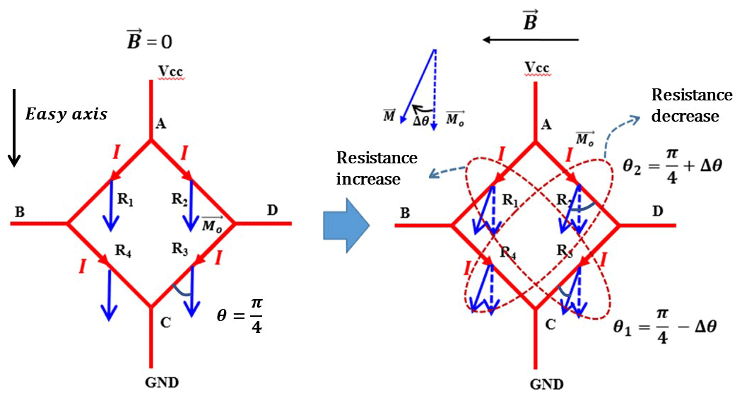
Figure 2PHR working principle of Wheatstone bridge structure. An external magnetic field (B) rotates the magnetization, generating the output signal proportional to the field.
2.1.2 Chip design of the PHR magnetic sensor
The Wheatstone bridge of the magnetic sensor is designed in a rhombus shape in which the power voltage is applied to the vertical axis, and the signal output is generated on the horizontal axis. In order to maximize the magneto-resistance value, a densely repeated pattern was drawn on a limited area of each quadrant (Figs. 3 and 4).
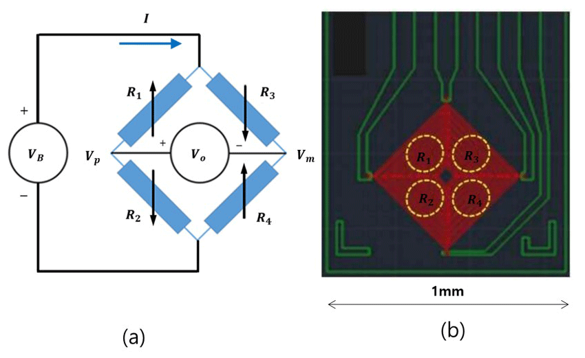
Figure 3PHR working principle of Wheatstone bridge structure. (a) Schematic circuit. (b) PHR sensor layout with a width of about 500 µm.
2.2 Manufacturing of the PHR magnetic-field sensor
The PHR magnetic sensor was fabricated with the following steps: thermal oxidation on a 4′′ silicon wafer, sputtering deposition of the magnetic thin film, Al signal line process, and passivation oxide deposition. The magnetic thin film is composed of three metal layers of NiFe–Cu–IrMn, in which the exchange interaction between NiFe and IrMn works through the Cu layer (Elzwawy et al., 2019; Sinha et al., 2013; Zhao et al., 2015; Spizzo et al., 2017).
2.3 Manufacturing of the pin-type current sensor probe
The diced PHR magnetic sensor chip from the fabricated wafer was attached to the PCB, wire bonded, and then assembled into a case manufactured by a 3D printer. Figure 4 shows the prototype current sensor probe, which has the circuit functions to amplify the sensor signal and control a sensor output offset and sensitivity.
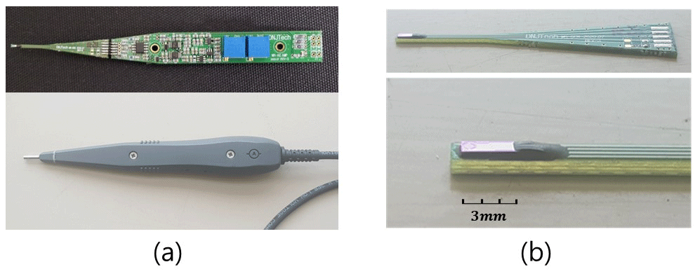
Figure 4(a) Assembled pin-type current probe and (b) enlarged sensor PCB of the current probe to which the PHR chip was attached and wire bonded.
3.1 Measurement system
The manufactured current probe can be connected to an indicator that displays the sensor output or to an oscilloscope for monitoring a current wave pattern (Fig. 5a). The indicator includes an analog–digital convert function to display the magnetic-field intensity or current flow value in a digital output. The indicator included a function to set a coefficient to convert the measured magnetic-field value to the current value. Performing a calibration process for each measurement environment could determine the conversion coefficient.
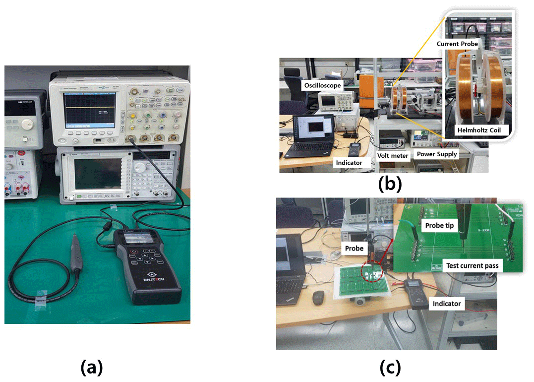
Figure 5Measurement systems. (a) Current probe and indicator. (b) Magnetic-field measurement setup using Helmholtz coil. (c) Current flow measurement setup using test PCB current line.
Figure 5b shows the experimental setup for measuring the magnetic-field-sensing performance. We used a Helmholtz coil that generated a magnetic field, a direct-current (DC) power supply, and a digital multimeter with high sensitivity for the measurement. The sensitivity of the magnetic field was measured by placing the current probe vertically at the center of the Helmholtz coil and detecting the generated magnetic field with a precision of 0.01 µT or less.
Figure 5c shows the experimental setup for measuring the current-sensing performance. In principle, it measures the strength of the magnetic field generated by a current. However, the signal intensity changes greatly depending on the distance and direction of the PCB current line from the probe. Therefore, to verify the consistent performance of the magnetic-field sensing, the probe's direction was set to be perpendicular to the current line, and the probe position was precisely adjusted to maintain the gap of 1 mm from the line.
3.2 Main characteristics of the current probe
Figure 6 is the result of repeating the measurements 10 times with intervals of about 0.01 µT to test the magnetic-field detection performance statistically. Based on this result, the null hypothesis (H0) and the alternative hypothesis (HA) were set as outlined below, and Student's t test was performed on two groups (0.049 and 0.057 µT groups) which showed the worst variances (Table 1).
-
H0 hypothesizes that there is no statistical difference between the two groups.
-
HA hypothesizes that there is a significant difference between the two groups.
As a result of the t test, the p value of the null hypothesis Ho is , which can be ignored entirely, compared to the significance level of α=0.05, which corresponds to the confidence level of 95 %. Therefore, the null hypothesis is rejected, and the alternative hypothesis that the magnetic-field resolution of 0.008 µT or less is significant can be adopted. In this study, although the results of only two groups are shown, the other eight groups also confirmed consistent results.
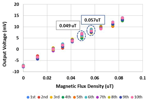
Figure 6Measurement result of magnetic-field-sensing resolution of 0.008 µT or less. The initial offset of about 7 mV in this figure was from the calibration error in the prototype current probe. Although it includes an internal offset calibration function controlled by a variable resistor, the variable resistor is difficult to control precisely. The offset calibration function may have an error in the millivolt (mV) region equivalent to the signal level of about 0.01 µT.
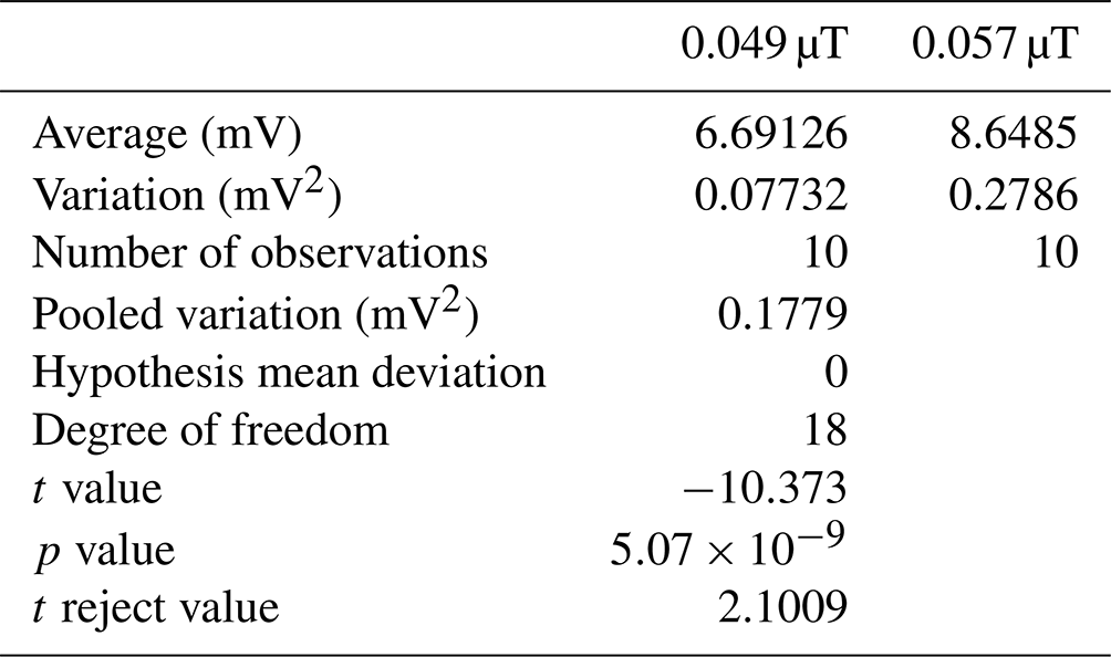
Figure 7 is the result of repeating the measurements 10 times with intervals of 1 mA to test the current detection performance statistically. Based on this result, the null hypothesis (H0) and the alternative hypothesis (HA) were set as outlined below, and Student's t test was also performed on two groups (7 and 8 mA groups) which showed the worst variances (Table 2).
-
H0 hypothesizes that there is no statistical difference between the two groups.
-
HA hypothesizes that there is a significant difference between the two groups.
As a result of t test, the p value of the null hypothesis H0 is 0.0018, which can be ignored entirely, compared to the significance level of α=0.05. Therefore, the null hypothesis is rejected, and the alternative hypothesis that the current-sensing resolution of 1 mA or less is significant can be adopted. Although the results of only two groups are shown, the other eight groups also confirmed consistent results.
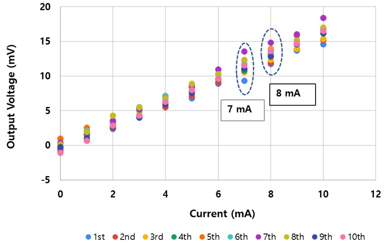
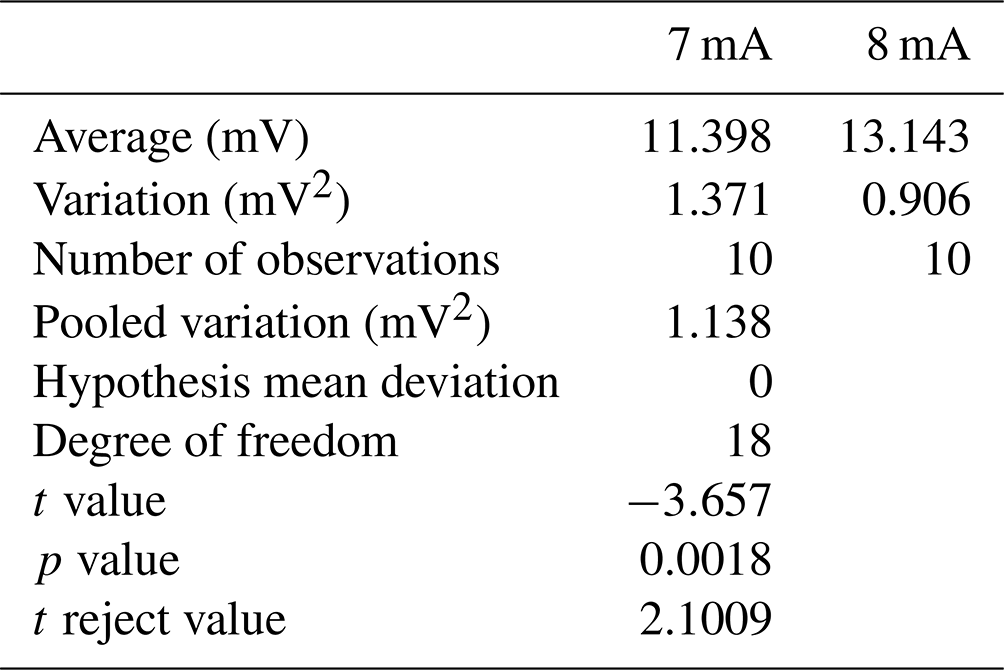
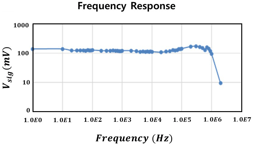
Figure 8 shows the frequency characteristics of the current probe. It can be seen that the operating characteristics are well maintained up to 1 MHz.
3.3 Thermal-offset drift issue of the current probe
During the characterization of the samples in Sect. 3.2, monotonous signal drift occurred during the initial operational stage just after the probes were turned on. Although the amplitude and the period differ from sample to sample, they all show the same pattern in which the output signal gradually drifts in time and becomes saturated within a few tens of minutes after starting its operation (Fig. 9). The amplitude of the drift offset could vary depending on the mismatch between the four resistors as the mismatch level might differ from sample to sample.
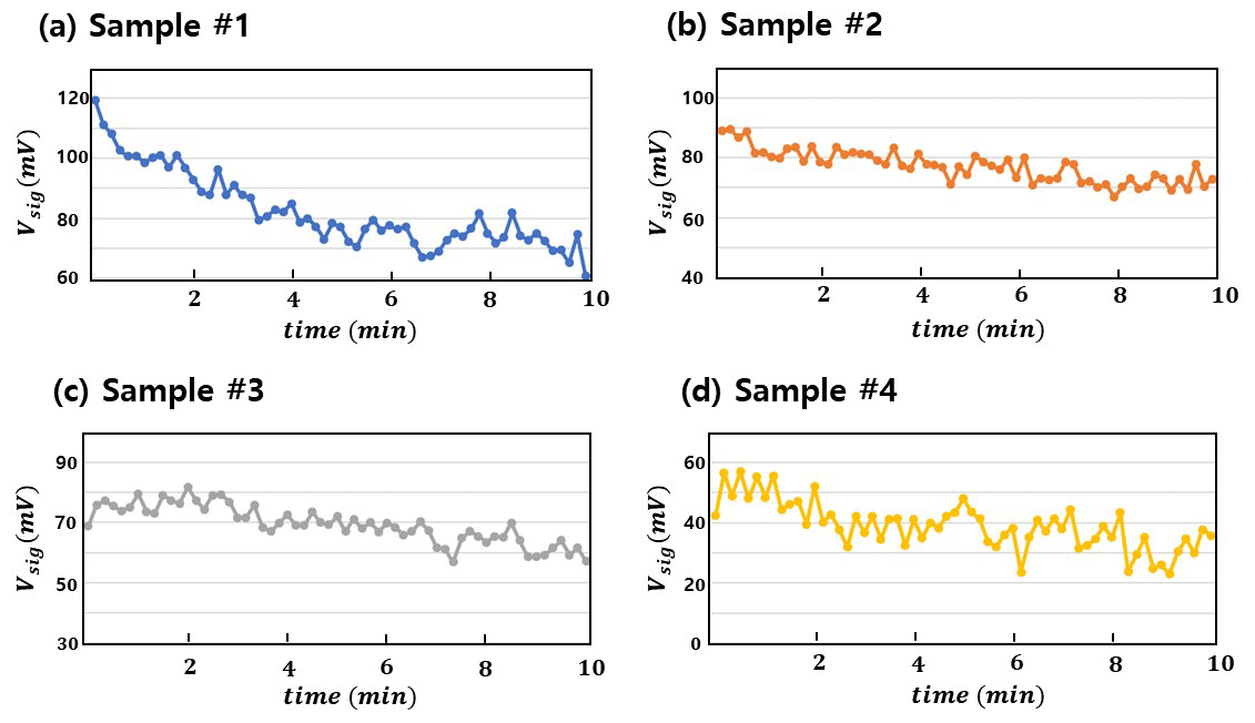
Figure 9Monotonously changing output signal drift at the initial turn-on stage of the current probe. The PHR resistance values are in 83±016 kΩ, and the sensor power VB=5 V.
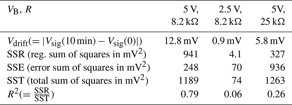
The leading causes of signal drift would likely be the changes in resistance due to Joule heating during the operation of the probe. Since Joule heating is essentially generated by electric power , we examined the effects on the signal drift according to the sensor power VB and the resistance value of the PHR sensor (Figs. 3 and 10). To quantitatively analyze this, we executed a regression analysis in Fig. 10 and summarized the results in Table 3. The offset drift (Vdrift), defined as the signal drift during the initial 10 min, decreased with an increase in resistance and a decrease in VB. When the resistance was increased to 25 kΩ, a slight drift of 5.8 mV occurred. However, for this sample, the determination coefficient (R2) of the regression is significantly lower than the baseline (8.2 kΩ), and the statistical significance of the drift is considered to be lower.
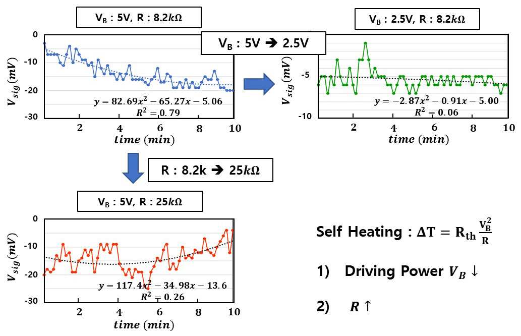
Figure 10Signal drift investigation with the changes of the sensor power VB and the PHR resistance values. Offset drift was reduced when VB was decreased and when the resistance values were increased.
Therefore, the signal drift can be interpreted as a phenomenon in which Joule heating increases the temperature at the sensor part as the sensor power is supplied, and the mismatch of the four PHR resistors intensifies according to the temperature-coefficient-of-resistance (TCR) effect. As a result, the monotonously changing signal drift appears to be the thermal-offset drift phenomenon caused by Joule heating at the PHR resistors.
Table 3Regression results of Joule-heating evaluation in Fig. 10.
The prototype current probe achieved the desired development target, but the thermal-offset drift occurred over the first few tens of minutes after starting its operation. Furthermore, since it is beyond the resolution limit of the probe, it needs to be improved. This chapter will theoretically identify the causes of thermal-offset drift and discuss the improvement plans.
The signal drift can originate from an ambient-temperature increase or Joule heating from the sensor operation. This phenomenon can be categorized into two cases. The first is the case where the temperature of the four PHR resistors rises uniformly due to an ambient-temperature increase or Joule heating (Sect. 4.1), and the other is the case where the temperature rises differently for each resistor because the amount of Joule heating is different with the resistance value (Sect. 4.2).
4.1 Uniform temperature increase (ΔT) in four resistors in the Wheatstone bridge
When the power VB is supplied to the sensor, the voltage signal of Vp node in Fig. 3 is as below:
If ambient temperature is changed by ΔT, the change of R1 and R2 is
where α is TCR.
Then, the change of the signal node voltage of Vp is as below:
In the same method,
In conclusion, there is no signal drift with a uniform temperature increase because the resistance ratio remains constant. Due to this effect, the sensors of a Wheatstone bridge structure can significantly suppress the typical temperature-dependent offset drift phenomenon. However, an offset drift can occur if there is a mismatch in the temperatures of the four resistors due to the difference in their values. This will be considered in the next section.
4.2 Different temperature increases in four resistors due to the mismatch between four PHR resistors
If the four PHR resistors in Fig. 3 are ideally identical, there is no offset of the output signal (Vo) in the absence of an external magnetic field. However, since there may be many variations in the manufacturing processes, an initial mismatch between the four resistors inevitably occurs. Depending on this initial mismatch, the output offset may exist under no external magnetic field, and this can cause thermal-offset drift. In the following, we will theoretically evaluate the possibility.
The signal drift can originate from Joule heating, occurring due to sensor operation and causing the mismatch increase due to the TCR effect. Depending on the resistance value, the amount of Joule heating in each resistor will be different, and the amount of temperature increase will also be different for each resistor. First, consider the mismatch between R1 and R2 at the node of Vp in Fig. 3:
where ϵ+ is the mismatch parameter between R1 and R2, considered to be infinitesimally small as follows:
At the initial stage of the sensor operating, since the same current I flows through R1 and R2, the signal voltage at the Vp node is divided according to the ratio of the resistance values, as below:
As the operating time elapses, Joule heating at the two resistors is released, and temperature increases as below:
where P1 and P2 are the power consumptions of R1 and R2, respectively; Rth is the thermal resistance of the sensor; and ΔT1 and ΔT2 are the temperature increases of R1 and R2, respectively.
Due to the Joule-heating difference as a result of the mismatch of the resistance values, the temperature difference, proportional to the mismatch parameter ϵ+, may occur. Due to this difference, the resistance mismatch becomes more distorted, as below:
where α is TCR.
By substituting the results of Eqs. (5) and (8) into Eq. (9), the changed mismatch according to the sensor operation is obtained by the first-order perturbation, as below:
where ΔT2 can be interpreted to be an overall temperature increase ΔT considering the infinitesimal mismatch.
Using the result of Eq. (10), the signal voltage of the Vp node drifts due to the different Joule heating between R1 and R2 during the sensor operation.
As a result, the signal drift may be as high as the last term in Eq. (11) during the sensor operation. If the temperature gradually increases due to Joule heating during the sensor operation, the signal drift may occur until the temperature is saturated after a few tens of minutes.
The signal voltage of the node of Vm in Fig. 3 can be obtained using the same method as below:
and
4.3 Solutions for thermal-offset drift
The phenomenon of temperature drift in Wheatstone-bridge-type current sensors has been reported in much of the literature (Vopalensky and Platil, 2012; Ramírez Muñoz et al., 2006; Kwiatkowski and Tumanski, 1986). For example, in the study by Vopalensky and Platil (2012), the authors investigated the differences in the temperature coefficient of signal offset and sensitivity when changing the sensor's power supply from a constant voltage source to a constant current source. Another technique reported in Ramírez Muñoz et al. (2006) involved compensating for the temperature coefficient of sensitivity by connecting a circuit based on a generalized impedance converter to the Wheatstone bridge. While these studies primarily analyzed the effects of overall temperature variations in the Wheatstone sensor, this report focuses on analyzing temperature differences in each resistance caused by the mismatch of resistance values within the Wheatstone bridge, which is considered to be the cause of thermal-offset drift.
According to the result of Eq. (11), we suggest the following three kinds of methods to improve the thermal-offset drift:
- 1.
reducing the mismatch ϵ itself
- 2.
reducing ΔT by applying pulse width modulation (PWM) on signal power
- 3.
lowering signal power VB.
Since the third method adjusts VB and can reduce the sensitivity of the magnetic sensor, we will mainly discuss (1) and (2) of the above solutions.
4.3.1 Actions for reducing the mismatch ϵ
1. Binning test to screen out the mismatching failure
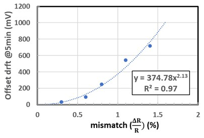
After setting the mismatch specifications of the overall mismatch to be less than 0.2 %, a binning test was performed to select the best-matched samples, which were used for manufacturing the prototypes. We confirmed that the samples with smaller mismatches showed better thermal-offset drift characteristics in Fig. 11. With the above criteria, the thermal-offset drift is estimated to be less than about 20 mV.
2. Sensor layout optimization for reducing the mismatch
The mismatch ϵ is fundamentally provoked by the process-loading effects, mainly in the lithography process and in the etch process for manufacturing the sensors. For example, the non-uniformity of plasma density in the etch process may cause the variation of the critical dimension (CD) for each pattern location (Plummer et al., 2020; Ki et al., 2000). In addition, it can deteriorate the mismatch of the four resistors and deepen the thermal-drift offset. This issue can be mitigated by splitting the layout of the four resistors and arranging them in a cross-intersecting manner to reduce the mismatch of each resistor, which will be the content of a future publication.
4.3.2 Reducing ΔT by applying pulse width modulation (PWM) to signal power
The third method to improve the thermal-offset drift is to suppress the temperature increase ΔT caused by the Joule heating. If the sensor power VB is lowered, the Joule heating is reduced, and ΔT is suppressed. However, the method may not be preferable because it can also deteriorate the sensitivity of the sensor output signal.
In this study, we introduce a method that uses the pulse width modulation (PWM) algorithm to supply sensor power VB. The PWM algorithm controls the sensor power VB that is to be supplied during the on-time (ton) of the sensor when it is measuring the signal and disconnected during the off-time (toff) of the sensor. Since the sensor power is supplied only during the ton time in this method, we expect that the average Joule heating will be reduced, and the thermal-offset drift can be improved.
Figure 12 shows the result of the PWM evaluation by reducing the duty ratio, defined by , from 100 % to 20 %. For the duty ratio of 20 % compared to 100 %, thermal-offset drift is dramatically reduced down to about (Table 4).
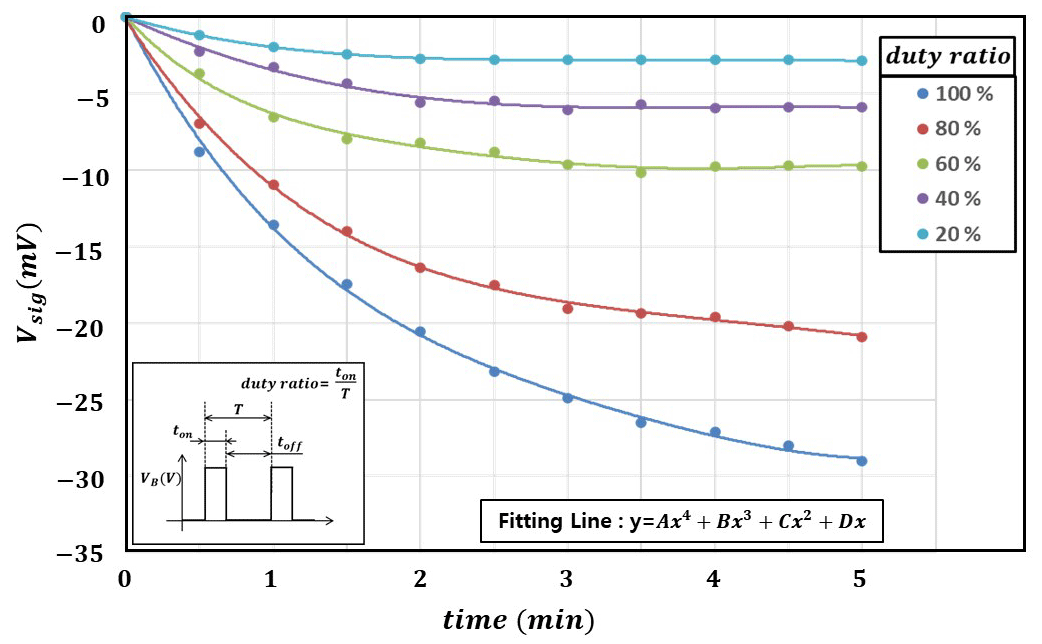
Figure 12PWM algorithm effect on reducing the thermal-offset drift. The thermal-offset drift is much more suppressed with the lower duty ratio.
Table 4Suppression of thermal-drift offset at 5 min as duty ratio decreases.
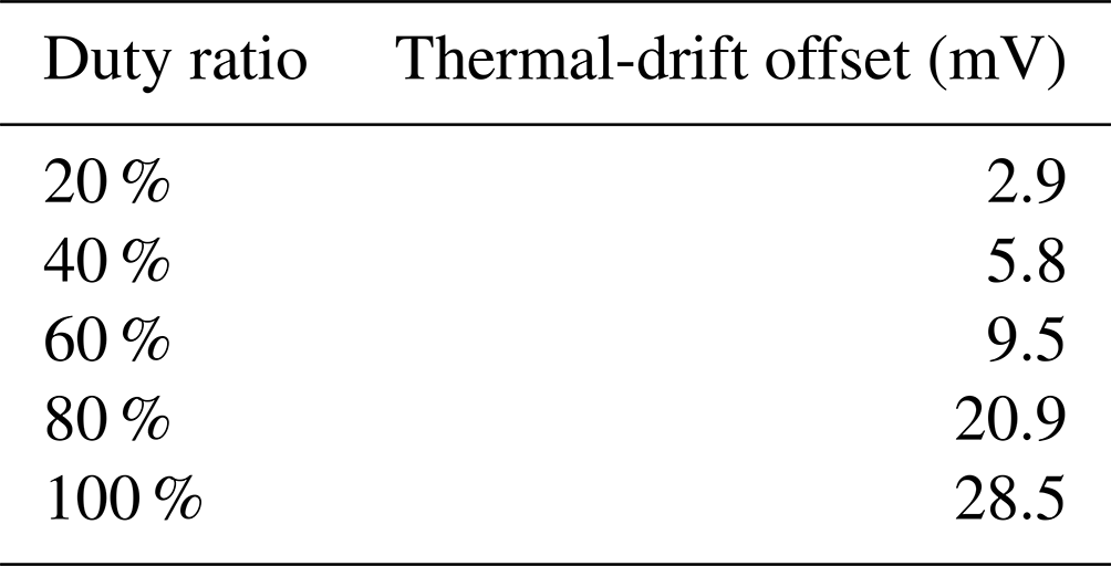
Satisfactory results have yet to be obtained when reducing the duty ratio to less than 20 %. However, we are in the process of improving the algorithm and have the plan to evaluate the measurement stability for a duty ratio of down to 1 %, and this will be reported in the future.
We developed a pin-type current probe with high sensitivity using PHR thin film, which is manufactured in a 4′′ Si wafer process. The developed sensor showed good-enough characteristics for analyzing highly integrated PCBs with 1 mA resolution on current measurements and up to 1 MHz operating frequency. During its characterization, however, we experienced a monotonously varying output signal in the time range of a few tens of minutes. We modeled this as the thermal-offset drift being caused by the mismatch between the four PHR resistors, suggested three methods to improve the offset, and reported some up-to-date evaluation results. Although the mismatch should be minimized, it cannot be completely eliminated due to fundamental process variations. Therefore, various methods other than those proposed in this study should be evaluated to suppress the thermal-offset drift. For example, there may be a method of reducing the thermal resistance value from the sensor to the outside. The results of these other methods might be reported through future studies.
All the data in this paper were generated by the authors and are available upon request.
NL conceived of the presented idea, developed the theory, and performed the data evaluations. JK verified the theory and data analysis, and DL supervised the sample preparation and findings of this work. All authors discussed the results and contributed to the final paper.
The contact author has declared that none of the authors has any competing interests.
Publisher’s note: Copernicus Publications remains neutral with regard to jurisdictional claims in published maps and institutional affiliations.
The authors gratefully acknowledge the financial support of the Ministry of MOTIE and the Ministry of SMEs and Startups, the Republic of Korea.
This work was supported by the Ministry of MOTIE and the Ministry of SMEs and Startups, the Republic of Korea (project nos. 20011264 and S2748201).
This paper was edited by Andreas Schütze and reviewed by two anonymous referees.
Chomsuwan, K., Yamada, S., and Iwahara, M.: Bare PCB inspection system with SV-GMR sensor Eddy-current testing probe, IEEE Sens. J., 7, 890–896, 2007.
Elzwawy, A., Kim, S. J., Talantsev, A., and Kim, C. G.: Equisensitive adjustment of planar Hall effect sensor's operating field range by material and thickness variation of active layers, J. Phys. D Appl. Phys., 52, 285001(1)–285001(19), 2019.
Hansen, M. F. and Rizzi, G.: Exchange-Biased AMR Bridges for Magnetic Field Sensing and Biosensing, IEEE T. Magn., 53, 1–11, 2017.
Huang, Y. and Wu, J. W.: Infrared thermal image segmentations employing the multilayer level set method for non-destructive evaluation of layered structures, NDT&E Int., 43, 34–44, 2010.
Ki, W. T., Yang, S. H., Moon, S. Y., Choi, S. W., Han, W. S., and Sohn, J. M.: A new correction method for dry etch loading effect in photomask fabrication, in: 2000 International Microprocesses and Nanotechnology Conference, Tokyo, Japan, 11–13 July 2000, IEEE, Sect. no. 11C-2-5, https://doi.org/10.1109/IMNC.2000.872613, 2000.
Koggalage, R., Chomsuwan, K., Yamada, S., Iwahara, M., and Abeyratne, U. R.: Giant magnetoresistance based Eddy-current sensor for High-speed PCB defect detection, in: Proceedings of the International Conference on Information and Automation, Colombo, Sri Lanka, 15–18 December 2005, University of Moratuwa, 170–175, 2005.
Kwiatkowski, W. and Tumanski, S.: The permalloy magnetoresistive sensors – properties and applications, J. Phys. E Sci. Instrum., 19, 502–515, 1986.
Plummer, J. D., Deal, M., and Griffin, P. B.: Silicon VLSI Technology: Fundamentals, Practice and Modeling, Chap. 10, US Ed, Pearson College Div., ISBN 0130850373, 2020.
Ramírez Muñoz, D., Sánchez Moreno, J., Casans Berga, S., Castro Montero, E., Reig Escrivà, C., and Navarro Antón, A. E.: Temperature compensation of Wheatstone bridge magnetoresistive sensors based on generalized impedence converter with input reference current, Rev. Sci. Instrum., 77, 105202, https://doi.org/10.1063/1.2358696, 2006.
Roh, Y. J., Park, W. S., and Cho, H.: Correcting image distortion in the X-ray digital tomosynthesis system for PCB solder joint inspection, Image Vision Comput., 21, 1063–1075, 2003.
Sinha, B., Hung, T. Q., Ramulu, T. S., Oh, S., Kim, K. W., Kim, D. Y., Terky, F., and Kim, C. G.: Planar Hall resistance ring sensor based on NiFe/Cu/IrMn trilayer structure, J. Appl. Phys., 113, 063903(1)–063903(5), 2013.
Spizzo, F., Tamisari, M., Chinni, F., Bonfiglioli, E., and Del Bianco, L.: Interface adjustment and exchange coupling in the IrMn/NiFe system, J. Magn. Magn. Mater., 421, 234–240, 2017.
Ueda, T., Oki, T., and Koyanaka, S.: An automated assessment method for integrated circuit chip detachment from printed circuit board by multistep binarization and template matching of X-ray transmission images, J. Mater. Cycles Waste, 23, 315–322, 2021.
Vopalensky, M. and Platil, A.: Temperature Drift of Offset and Sensitivity in Full-Bridge Magnetoresistive Sensors, IEEE T. Magn., 49, 136–139, 2012.
Zhang, J. Y., Xu, W., Zhang, W., Meng, X., and Zhang, Y.: A novel compression algorithm for infrared thermal image sequence based on K-means method, Infrared Phys. Techn., 64, 18–25, 2014.
Zhao, Z. D., Li, M. H., Kang, P., Zhao, C. J., Zhang, J. Y., Zhou, L. J., Zhao, Y. C., Jiang, S. L., and Yu, G. H.: The influence of ultrathin Cu interlayer in NiFe/IrMn interface onrotation of the magnetic moments, Appl. Surf. Sci., 332, 710–715, 2015.