the Creative Commons Attribution 4.0 License.
the Creative Commons Attribution 4.0 License.
 | 06 Feb 2025
Effects of potassium sodium niobate (KNN) thickness on biaxial non-resonant microelectromechanical systems (MEMS) mirror performance
Christel Dieppedale
Antoine Hamelin
Romain Liechti
Gwenael Le Rhun
This work presents the results obtained with potassium sodium niobate (KNN) biaxial non-resonant microelectromechanical systems (MEMS) mirrors manufactured on a 200 mm silicon substrate. These MEMS mirrors feature various reflector dimensions for the squared shape, ranging from 0.5 × 0.5 to 2 × 2 mm2, and incorporate sputtered potassium sodium niobate ((K0.35Na0.65)NbO3) thin-film piezo-motors from Sumitomo Chemical, with thicknesses varying from 0.5 to 1.5 µm. A comparison of the mirror's performance and static deformation as a function of KNN thickness will be presented and discussed. The results obtained with these non-resonant mirrors, all fabricated using a collective 200 mm silicon manufacturing process, exhibit the following: (a) an arm deformation of 50 to 80 µm corresponding to an estimated tensile residual stress of approximately 120 MPa in the KNN layer, (b) the same level of performance for the 0.5 µm thick lead zirconate titanate (PZT) and KNN at 10 V, and (c) an optical angle up to 8.5° at 40 V for the 2 × 2 mm2 mirror design with 1.5 µm thick KNN. These results indicate that the MEMS mirrors fabricated with the KNN lead-free piezoelectric material offer state-of-the-art performances and open potential applications in a wide range of fields from light detection and ranging (lidar) systems to biomedical applications, thanks to the full biocompatibility of the KNN material.
- Article
(2352 KB) - Full-text XML
- BibTeX
- EndNote


Microelectromechanical systems (MEMS) mirrors are widely used in a variety of applications due to their compact size, affordability, and minimal power consumption compared to traditional mechanical scanning systems (Holmstrom et al., 2014). These applications include projection display systems for augmented reality (AR) and virtual reality (VR) smart glasses (Urey et al., 2013), biological imaging (Liu et al., 2014), and light detection and ranging (lidar) systems (Wang et al., 2020) (among others). Piezoelectric actuation is emerging as a promising choice, offering significant advantages such as high force, low voltage requirements, high-frequency capability, and fast response times. For such applications, lead zirconate titanate (PZT) has been recognized as the leading piezoelectric material, distinguished by its competitive electromechanical coupling and high piezoelectric coefficient (Tsaur et al., 2002).
In the field of long-range lidar applications, we have previously developed 2D MEMS mirrors incorporating PZT piezoelectric actuators on 200 mm silicon wafers, taking advantage of VLSI (very-large-scale integration) technology (Mollard et al., 2023). This method enables a collective and monolithic approach, thereby reducing costs. We carried out tests on different mirror diameters, including reflector diameters of 0.5 × 0.5, 1 × 1, and 2 × 2 mm2, corresponding to footprints of 2.5 × 2.5, 4 × 4, and 8 × 8 mm2, respectively. These biaxial mirrors are designed for non-resonant operation and feature a symmetrical configuration with four suspended actuators. However, the environmental impact of the lead present in the PZT is raising serious concerns, both for the environment and for human health (Panda, 2009). Consequently, legislation has been enacted in numerous countries to prohibit the use of lead with some temporary exceptions (Tsinaraki et al., 2020). To replace PZT actuators, various families of lead-free piezoelectric materials are being developed (Aspe et al., 2018; Barbatoa et al., 2021; Gu-Stoppel et al., 2020). Among these, potassium sodium niobate (KNN) emerges as particularly promising due to its elevated Curie temperature and high piezoelectric coefficient. Moreover, KNN materials exhibit excellent biocompatibility with cells, showcasing significant potential for biomedical applications (Gaukås et al., 2020). We have previously demonstrated the first KNN biaxial non-resonant MEMS mirrors (Kuentz et al., 2024), manufactured on a 200 mm silicon substrate, integrating a 1 µm sputtered potassium sodium niobate ((K0.35Na0.65)NbO3) thin film from Sumitomo Chemical. The KNN film and electrodes exhibit good performances with high piezoelectric coefficient and permittivity, whereas optical angles of up to 6.3° at 200 Hz frequency for the 2 × 2 mm2 mirrors have been obtained. These results are the state of the art compared to the results previously obtained.
In this paper, we present the performance obtained using different thicknesses for the KNN motor, namely 0.5, 1, and 1.5 µm, all deposited by Sumitomo Chemical (Shibata et al., 2022). These mirrors are fabricated on a 200 mm silicon substrate. Firstly, we examine the mirror deformation and deduce an approximate value of the internal stress of KNN. Secondly, we present a comparison of mirror performance between KNN and PZT at a thickness of 0.5 µm, followed by a performance comparison of mirrors using KNN motors of 0.5, 1, and 1.5 µm. We will also discuss the results and compare them with analytical models.
The fabrication of the 2D mirror was carried out on a (100) 200 mm silicon-on-insulator (SOI) substrate, featuring a 20 µm thick silicon layer, a 1 µm thick buried oxide layer, and a 725 µm thick silicon handle wafer. Subsequently, KNN films with a composition of (K0.35Na0.65)NbO3 and thicknesses of 0.5, 1, and 1.5 µm were deposited onto these platinized 200 mm SOI wafers via sputtering by Sumitomo Chemical, following a previously documented process (Shibata et al., 2022). After the KNN deposition covered with RuO2 / Pt bilayer electrode materials, the layer stack was arranged from bottom to top as follows: Si (725 µm) / SiO2 (1 µm) / Si (20 µm) / SiO2 (500 nm) / ZnO (25 nm) / Pt (200 nm) / KNN (0.5, 1, or 1.5 µm) / RuO2 (30 nm) / Pt (100 nm). The KNN-based wafers were then processed in the MEMS clean room at CEA-LETI utilizing a generic mask set comprising nine lithographic levels. The technological process is fully described in Kuentz et al. (2024). Figure 1 illustrates a schematic cross-section view of the layer stack, while Fig. 2 displays a picture of a full 200 mm wafer and a top view of a 1 µm thick KNN MEMS mirror at the completion of this process.
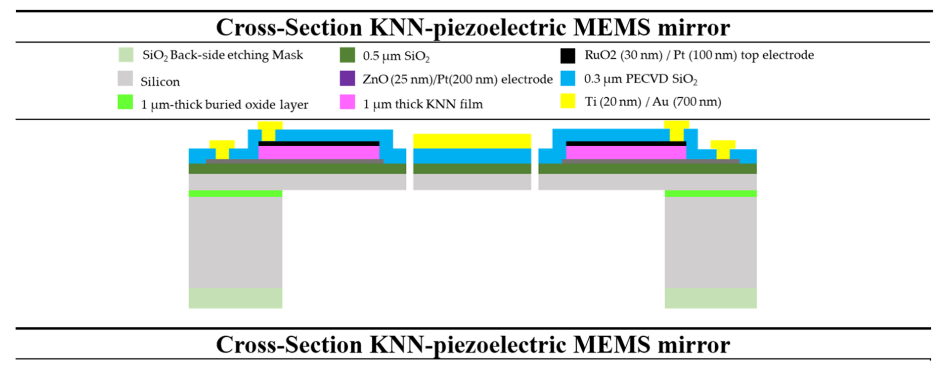
Figure 1Cross-section of KNN piezoelectric MEMS mirror (note that PECVD represents plasma-enhanced chemical vapor deposition).
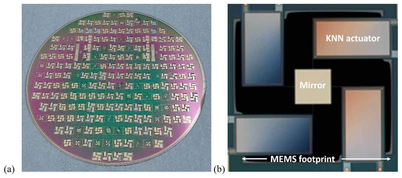
Figure 2The 200 mm silicon wafer of the KNN MEMS mirror (a) and the top view of the MEMS mirror (b).
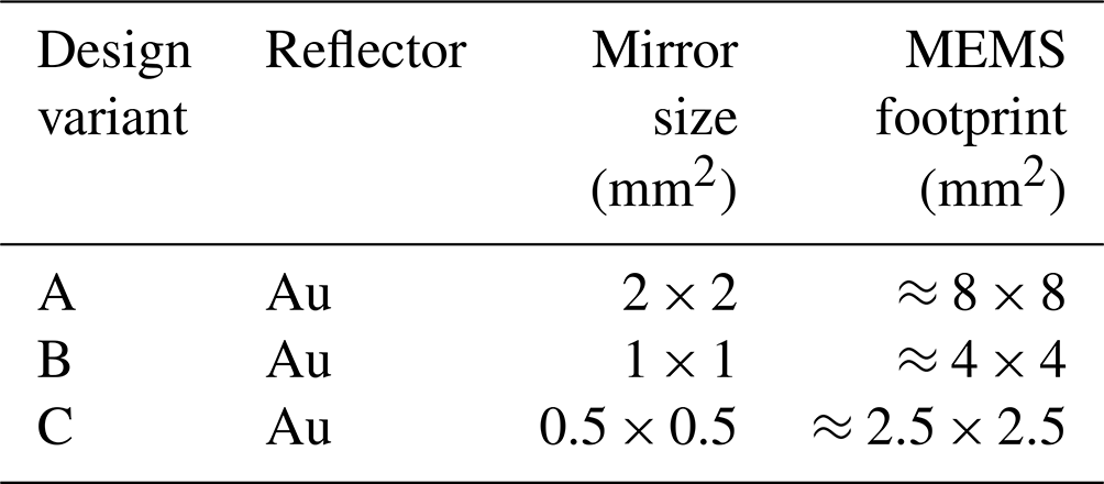
Dielectric and piezoelectric characterizations of fully integrated capacitors across entire wafers have been previously documented (Kuentz et al., 2024) for 1 and 1.9 µm thick KNN, yielding the following performance characteristics. The 1 µm KNN piezoelectric material demonstrates a high permittivity (ε) of approximately 1200 and an indirect piezoelectric coefficient (d31), extracted from cantilever deflection values, near 130 pm V−1. Three mirror designs were studied with the main specifications provided in Table 1.
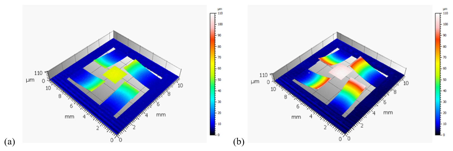
Figure 3Mirror deformation along the Z axis near ambient temperature (30 °C) – design variant A with 0.5 µm (a) and 1 µm thick KNN (b); no driving voltage.
Residual stresses within the multilayer stack could result in the KNN mirror being not perfectly flat. Knowledge of the mirror arm deformation appears to be a key parameter as it defines the initial Z position shift, without polarization, of the mirror. This point can be key to the alignment of the laser and the detector at the system level. Furthermore, in the case of a non-symmetrical mirror, e.g. with different arm lengths, the deflection may vary, causing an initial tilt of the mirror. Typically, post-manufacture, either a concave or convex distortion in the mirror and beam is observed. The mirror's Z deformation was assessed utilizing an Altisurf 520 tool from Altimet (France). Figure 3 provides an overview of the mirror's deformation along the Z axis at 30 °C and under atmospheric pressure. No voltage was applied during the measurement. The analysis includes two design variants, with KNN thicknesses of 0.5 and 1 µm. This Z deflection reaches a value of 50 µm (δ0.5 µm) with a KNN thickness of 0.5 µm and increases to 80 µm (δ1 µm) when the KNN thickness is doubled to 1 µm.
Figure 4 shows the evolution of the Z deflection of the mirror arms as a function of KNN thickness. This evolution is compared with published analytical models of multilayers (Hsueh, 2002; Defaÿ, 2011), where the radius of curvature of a multilayer beam can be estimated using the following formula:
where αi and αs represent the thermal expansion coefficients of the film (i) and substrate (s), respectively. and represent their biaxial elastic moduli, ϑi and ϑs represent the Poisson ratios, and ΔT is the temperatures difference between deposition and operation. ti (0.5 µm or 1 µm) and ts (20 µm) refer to the thickness of the layer (i) and substrate (s), respectively. This equation is a first-order approximation that excludes terms with orders higher than ti. This omission is consistent with the ti layer thicknesses being at least 20-fold thinner than the substrate thickness ts. These models also fail to consider any bending moment exerted on the actuators. However, this assumption does not hold true in our case, as the cantilevers are connected to the mirror. Nonetheless, it provides a preliminary estimation of the anticipated deformation.
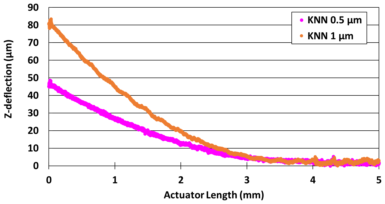
Figure 4The Z deflection of the KNN actuator with 0.5 and 1 µm thick KNN – design variant A.
A direct calculation of the radius of curvature, using Eq. (1), is not possible, because all the multilayer characteristics (especially Ei and αi) are not precisely known. However, as reported in Shibata et al. (2009), we could use the evolution of the Z deflection of the KNN actuator, with 0.5 and 1 µm thick KNN, reported in Fig. 4, to estimate the residual stress of KNN.
Considering that the residual stress for the KNN layer is the same with the 0.5 and 1 µm depositions, we can write
where r0.5 µm and r1 µm are the radii of curvature with 0.5 and 1 µm thick KNN, and tKNN is the 0.5 µm thick KNN added between the two multilayers present in Fig. 4.
Additionally, as reported in Hsueh (2002), the thermal stress between a film (i) and a substrate (s) is
In a first approach (Defaÿ, 2011), the radius of curvature (r) of the KNN actuator can be deduced from its maximum Z deflection (δ), knowing the length of the KNN cantilever (L = 3.93 m in our case):
And Eq. (2) can be written as follows:
As mentioned in Dahl-Hansen et al. (2018), assuming to be 236 GPa (with Esi=170 GPa and ϑsi=0.28), we calculate a tensile stress of 123 MPa for the KNN layer. This value surpasses the 53 MPa reported in Shibata et al. (2022) but remains coherent when considering the approximations made. Additionally, this tensile value is comparable to those previously published for the PZT material (Damjanovic, 1998), which indicates a deformation of the same order at equivalent thickness. This approximate value of the residual stress in KNN, obtained from experimental measurements, will enable us to simulate and predict the expected deformation of other MEMS mirrors incorporating KNN. Additional measurements need to be done in future to confirm these results.
Following the study on residual stress, the performances in terms of 2D scan figures were evaluated on the KNN components at 30 °C and under atmospheric pressure. Characterizations were conducted using a sinusoidal waveform of 200 Hz for the fast axis and a 4 Hz ramp for the slow axis, with an experimental set-up previously presented (Mollard et al., 2023). These frequencies were selected to prevent the excitation of the rotational mode, ensuring a significant distance from the previously measured resonance frequency. The 2D scanning figures are illustrated with 50 points within a 200 Hz period (f). The horizontal (x) and vertical (y) axes represent the fast and slow axes, respectively.
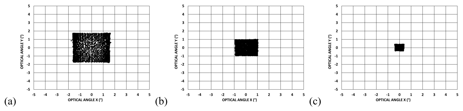
Figure 5The 2D scanning representation of the 0.5 µm thick KNN MEMS mirror (10 V, 200 Hz fast/horizontal axis, and 4 Hz ramp slow/vertical axis), with (a) design variant A, (b) design variant B, and (c) design variant C.
Table 2Comparison of θe, fe, and figure of merit (FoM), measured in this work for design variants A, B, and C with the 0.5 µm thick KNN and PZT (voltage of 10 V).
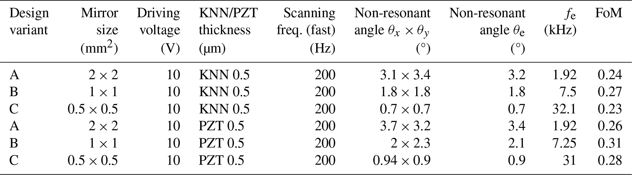
The results for design variants A to C with a 0.5 µm thick KNN are presented in Fig. 5. The maximum voltage across the KNN is constrained, in a first step, to 10 V, with for the fast sinusoidal axis. This voltage restriction arises from some capacitive breakdown observed in the 0.5 µm thick KNN actuator at higher voltage levels. Investigating the causes and occurrences of such breakdown needs to be explored in both integrated material or mirror design. Notably, no such issues were encountered with the 1 and 1.5 µm thick KNN layers. The optical angles θx and θy for the three mirror designs are detailed in Table 2, and compared with the corresponding values obtained under identical conditions using a 0.5 µm thick PZT layer. The measurements of θx and θy are conducted at y=0 and x=0, respectively, with an uncertainty of ±0.2° attributable to experimental set-up variations.
In Table 2, these results are compared with previously reported data (Wang et al., 2020) using a figure of merit (FoM) that integrates the key-parameters. The FoM is defined as , with θe (rad) the effective optical scanning angular field of view, de (mm) the effective dimension of the mirror and fe (kHz) the effective resonant frequency of the MEMS mirror. The values computed for the FoM are presented alongside previous results obtained with 2D non-resonant scanning MEMS mirrors utilizing various actuation motors such as electrostatic, electromagnetic, thermal and piezoelectric. Table 2 and Fig. 6 clearly demonstrate that the results, obtained for the same mirror design and silicon thickness, using 0.5 µm thick KNN and PZT, exhibit similar performance levels. Albeit a slight increase in field of view (FoV) for the PZT (between 10 % to 20 %), the differences are not substantial. This difference could be attributed to the indirect piezoelectric coefficient (d31) with a mean value near 130 pm V−1 for the KNN layer (Kuentz et al., 2024) and 150 pm V−1 for the PZT in our case (Mollard et al., 2023). It has to be noticed that higher value of d31 has been reported for PZT depending on process (Abergel et al., 2012).
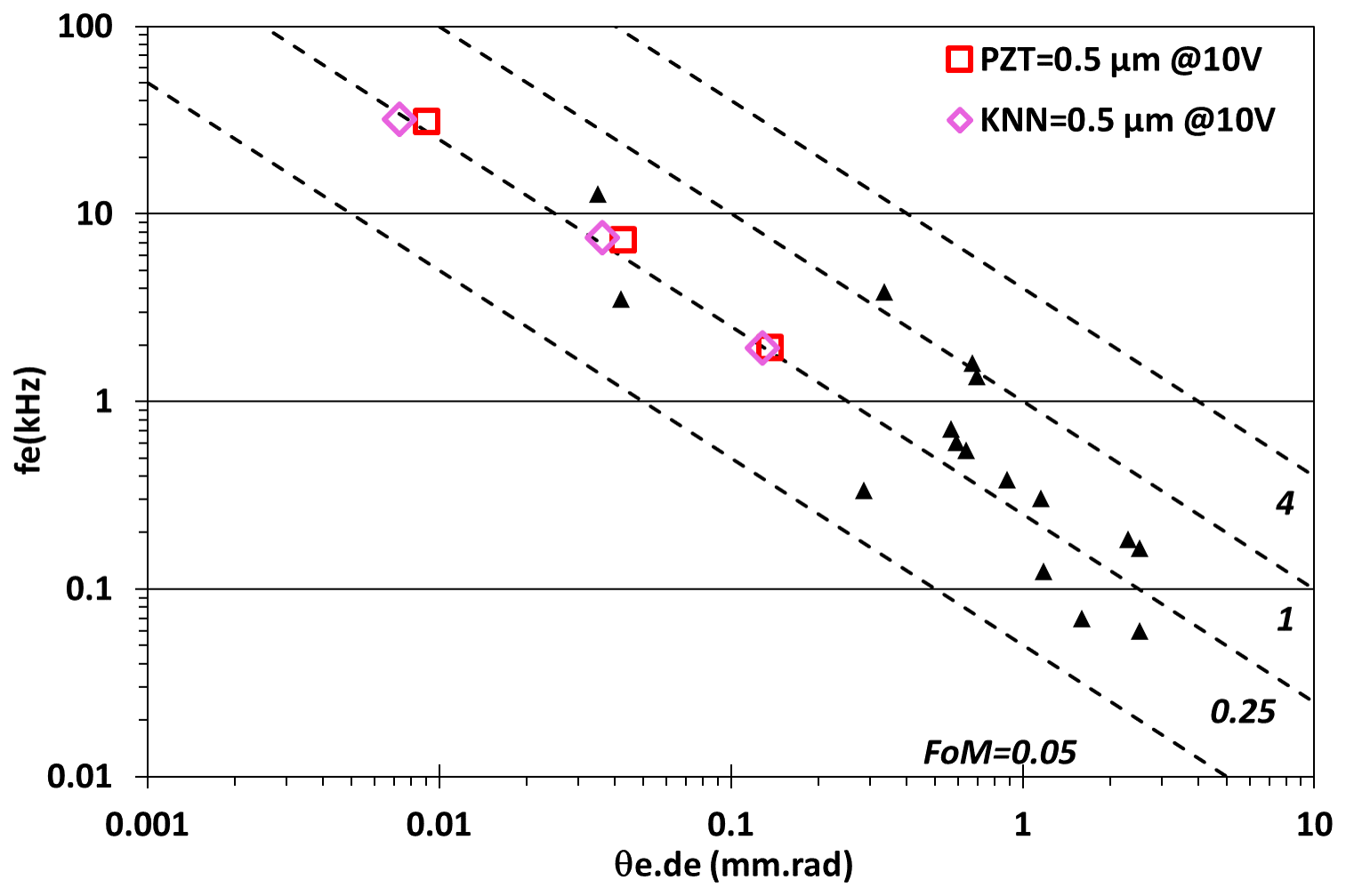
Figure 6FoM values previously reported in Wang et al. (2020) (black triangles) and this work for the 0.5 µm thick PZT (red squares) and as pink diamonds for the 0.5 µm thick KNN.
Table 3Comparison of θe, fe, and FoM, measured in this work for design variants A, B, and C with the 1 µm thick KNN (20 V voltage) and the 1.5 µm thick KNN (30 V voltage).
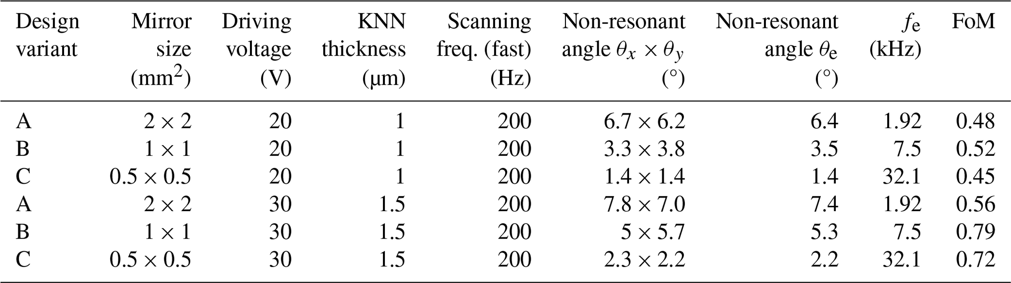
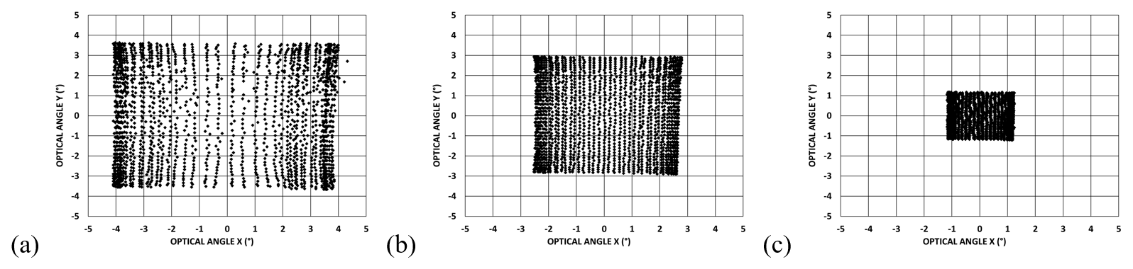
Figure 7The 2D scanning representation of the 1.5 µm thick KNN MEMS mirror (20 V voltage, 200 Hz fast/horizontal axis, and 4 Hz ramp slow/vertical axis), with (a) design variant A, (b) design variant B, and (c) design variant C.
However, if we compare these results with previous data, they do not rank among the best, largely because of the limitations imposed by the driving voltage. To pursue this, additional tests have been conducted with higher driving voltages on thicker KNN layers, i.e. 1 and 1.5 µm thick. In a first approach, the deflection of the mirror results from the movement of the KNN actuators, which are directly related to the effective transverse piezoelectric coefficient e31,f. The piezoelectric stress (σP) can be expressed as (Dahl-Hansen et al., 2018), where Ez is the transverse electric field (V m−1), i.e. the driving voltage (V) divided by KNN actuator thickness. A performance comparison between the different KNN thicknesses has been conducted using identical transverse electric field, Ez =200 kV cm−1 inside the KNN layer, achieved by adapting the driving voltage. The results are presented in Fig. 7 and Table 3 and are compared with previously reported results in Fig. 8.

Figure 8FoM values previously reported in Wang et al. (2020) (black triangles) and this work – pink diamonds for the 0.5 µm thick PZT (10 V voltage), blue diamonds for the 1 µm thick KNN (20 V voltage), and red diamonds for the 1.5 µm thick KNN (30 V voltage).
As shown, a clear increase in mirror performance is observed when increasing KNN thickness (and so driving voltage). No capacitive breakdown is observed when using 1 or 1.5 µm thick KNN. Results obtained with 1 and 1.5 µm show state-of-the-art results with an FoM value near 0.8 in the best case for a limited 30 V driving voltage.
These results have to be compared via existing analytical models, as presented in Liechti et al. (2024). The simulation model used to predict the behaviour of biaxial MEMS mirrors is based on a lumped element formulation. This model has been previously used to predict the behaviour of PZT 2D MEMS mirrors. In the model, the mirror is considered a longitudinal assembly of three deformable beams, as depicted in Fig. 9. The length along x is normalized over the total length L such that .
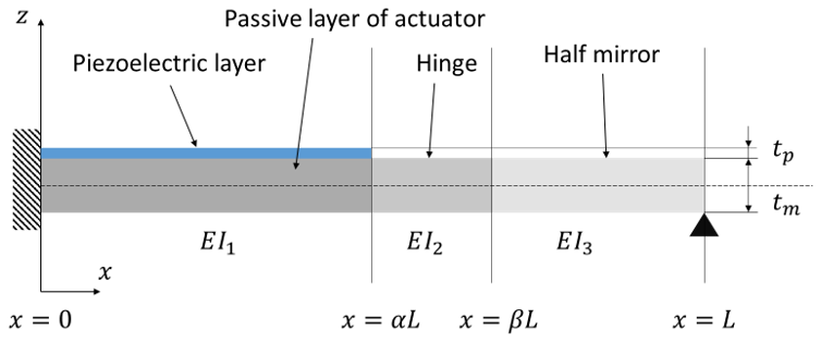
Figure 9Schematic representation of the assembly of beams, representing half of one axis of the mirror; adapted from Liechti et al. (2024).
The first beam consists of an assembly of a passive layer, representing the silicon layer, and an active layer, representing the piezoelectric layer. An equivalent Young's modulus and moment of inertia are calculated to simulate the actuator beam as a single equivalent beam. The action of the piezoelectric layer is simulated as a longitudinal force multiplied by the distance from the middle of the piezoelectric layer to the neutral line. Effects of other layers, such as the electrodes, are neglected. The second beam represents the hinge, and the third beam represents the mirror, whose Young's modulus multiplied by the moment of inertia is far larger than that of the other beams, i.e., EI1≪EI3 and EI2≪EI3. The displacements of each section of the beams are then written as
where M1 refers to the piezoelectric layer, M2 to the hinge, and M3 to the half mirror. By imposing no displacement and no rotation at x=0 and a free rotation with no displacement at x=L (the end of the assembly, representing the centre of the mirror), an explicit expression can be derived for δ0, i.e. the free displacement of the edge of the mirror at x=βL, and is written as
This displacement is then converted to a rotation angle of the mirror. More details are available in Liechti et al. (2024).
As shown in Fig. 10, we obtained a good correlation between the measured and simulated data for design variants A to C using a similar transverse field of Ez = 200 kV cm−1. However, we note that the simulation tends to overestimate performance in the case of design variant A, i.e. for the larger-diameter mirror.
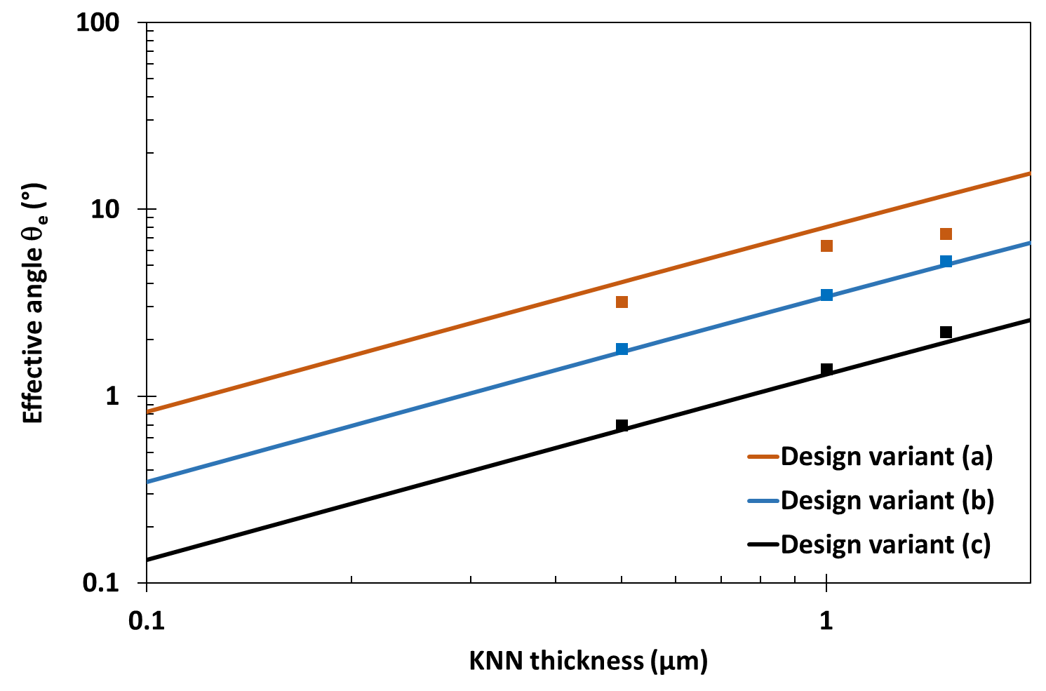
Figure 10Comparison of θe between measured (black square) and simulated data (lines) for design variants A, B, and C with Ez = 200 kV cm−1.
Table 4Comparison of θe, fe, and FoM, measured in this work for design variant A with 0.5, 1, and 1.5 µm thick KNN at voltages of 10 and 20 V.
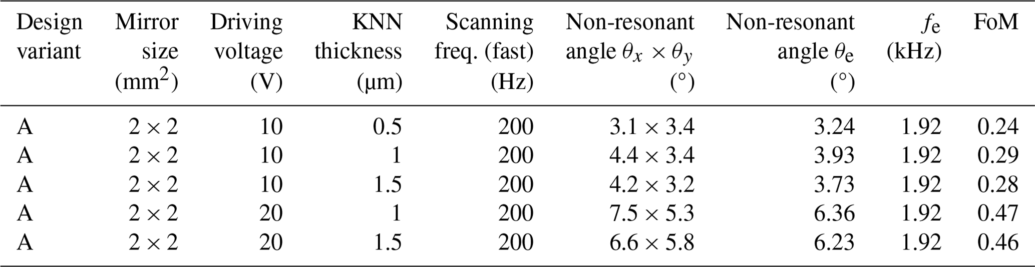
Additionally, Table 4 and Fig. 11 show the evolution of θe (°) for design variant A, i.e. a square mirror of 2 × 2 mm2, as a function of KNN thickness at supply voltages of 10 and 20 V.
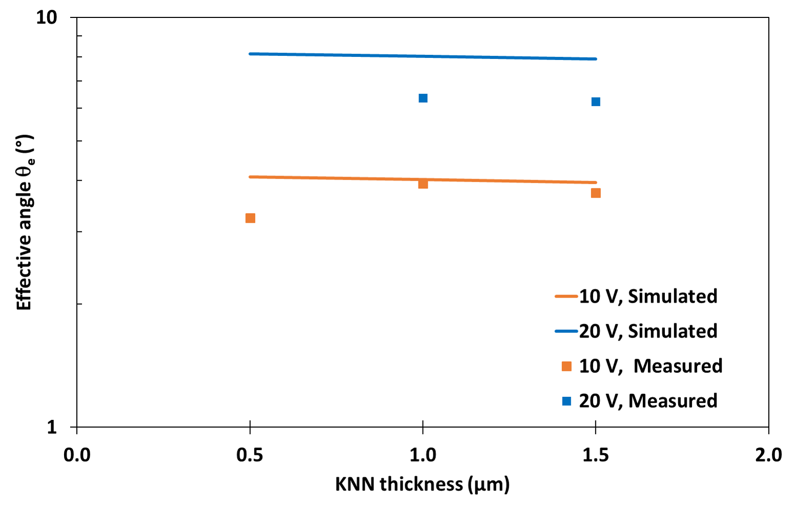
Figure 11Evolution of θe with KNN thickness measured and simulated data at 10 and 20 V – design variant A.
Different points can be highlighted. Firstly, experimental and simulated data clearly show that increasing the KNN thickness at the same voltage induces a limited decrease in the optical angle. Secondly, the performances are slightly lower for the 0.5 µm thickness at 10 V than predicted by the simulation. Finally, the performances of the mirrors at 20 V are overall lower than expected. Doubling the voltage results in a between 60 % to 70 % increase in the θe angle, not a doubling, highlighting the limitation of the model. Further studies are needed to investigate these points.
Table 5θe, fe, and FoM, measured in this work for design variant A with 1.5 µm thick KNN at a voltage of 40 V.
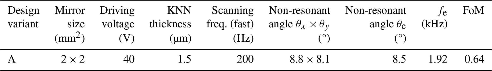
The last characterization involved increasing the driving voltage to the maximum one achievable with our experimental set-up, i.e. 40 V. This test has been done with the 1.5 µm thick KNN and design variant A. The results, presented in Table 5 and Fig. 12, show that an angle of 8.5° was achieved, corresponding to a FoM of 0.64. These results represent clear state-of-the-art performances compared to the best results previously obtained with a non-resonant biaxial mirror.
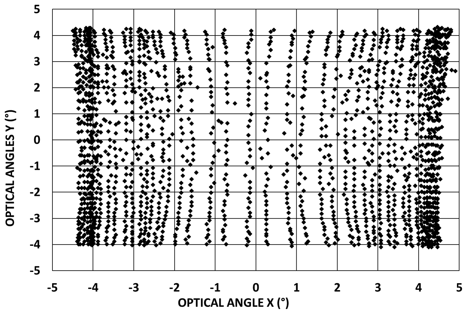
Figure 12The 2D scanning representation of the 1.5 µm thick KNN MEMS mirror – design variant A (40 V, 200 Hz fast/horizontal axis, and 4 Hz ramp slow/vertical axis).
This work reports on the performance of KNN biaxial non-resonant MEMS mirrors manufactured on a 200 mm silicon substrate. Three KNN thicknesses, ranging from 0.5 to 1.5 µm, were studied on the mirror with reflector diameters ranging from 0.5 × 0.5 to 2 × 2 mm2. Firstly, Z deformation measurements, performed on MEMS mirrors with 0.5 and 1 µm thick KNN motors, enabled the estimation of the residual stress in the KNN layer to be approximately 120 MPa, which is consistent with previously published values. Secondly, a comparison of the performance of the 2 × 2 mm2 mirrors, using the FoM = criteria, was conducted with both 0.5 µm thick PZT and KNN piezoelectric motors. It showed that both types of piezoelectric layers achieved similar performance levels at 10 V. It should be noted that some capacitive breakdown was observed on the KNN mirrors, which was not encountered with the thicker KNN layers. Further studies on the ageing of the KNN motor should be conducted and compared with existing research. Thirdly, a comparison of mirror performance based on the thickness of the KNN motor was carried out, showing consistent performance levels at identical driving voltages. As predicted by first-order analytical models, the driving voltage emerged as the primary factor influencing mirror performance. Advanced analytical models need to be developed to better fit the mirror's behaviour. Finally, the driving voltage was increased to 40 V, with the 1.5 µm thick KNN, achieving an optical angle of 8.5° and a FoM of 0.64, which is comparable to results obtained in previously published data. Additional measurements must be conducted at higher voltages to define the voltage limit as a function of thickness. This study thus highlights the development of lead-free KNN mirrors fabricated using 200 mm silicon technology, opening up applications in fields such as biomedical applications and other areas where the use of lead-based piezoelectric materials could be a limitation.
All the codes are not publicly available but can be made available upon reasonable request to the corresponding author.
All the measurement data are not publicly available but can be made available upon reasonable request to the corresponding author.
LM: conceptualization, methodology, investigation, writing (original draft), writing (review and editing), project administration, visualization. CD: investigation, writing (review and editing). AH: validation, investigation, writing (review and editing). GLR: investigation, writing (review and editing). RL: investigation, writing (review and editing)
The contact author has declared that none of the authors has any competing interests.
Publisher's note: Copernicus Publications remains neutral with regard to jurisdictional claims made in the text, published maps, institutional affiliations, or any other geographical representation in this paper. While Copernicus Publications makes every effort to include appropriate place names, the final responsibility lies with the authors.
The authors are thankful to Sumitomo Chemical for depositing KNN films with electrodes on the SOI wafers.
This work is part of the IPCEI Microelectronics and Connectivity project and was supported by French public authorities within the frame of France 2030.
This paper was edited by Michael Kraft and reviewed by two anonymous referees.
Abergel, J., Allain, M., Michaud, H., Cueff, M., Ricart, T., Dieppedale, C., Le Rhun, G., Faralli, D., Fanget, S., and Defay, E.: Optimized gradient-free PZT thin films for micro-actuators, in: 2012 IEEE International Ultrasonics Symposium, 2012 IEEE International Ultrasonics Symposium, 7–10 October 2012, Dresden, Germany, 972–974, https://doi.org/10.1109/ULTSYM.2012.0243, 2012.
Aspe, B., Cissé, F., Castel, X., Demange, V., Députier, S., Ollivier, S., Bouquet, V., Joanny, L., Sauleau, R., and Guilloux-Viry, M.: KxNa1−xNbO3 perovskite thin films grown by pulsed laser deposition on R-plane sapphire for tunable microwave devices, J. Mater. Sci., 53, 13042–13052, https://doi.org/10.1007/s10853-018-2593-9, 2018.
Barbatoa, P. S., Casuscellib, V., Apreaa, P., Scaldaferrib, R., Pedacib, I., and Caputoa, D.: Green production of lead-free bzt-bct thin films for applications in mems devices, Chem. Engineer. Trans., 84, 97–102, 2021.
Dahl-Hansen, R. P., Tybell, T., and Tyholdt, F.: Performance and reliability of PZT-based piezoelectric micromirrors operated in realistic environments, in: 2018 IEEE ISAF-FMA-AMF-AMEC-PFM Joint Conference (IFAAP), 2018 IEEE ISAF-FMA-AMF-AMEC-PFM Joint Conference (IFAAP), 27 May–1 June 2018, Hiroshima, Japan, 1–4, https://doi.org/10.1109/ISAF.2018.8463243, 2018.
Damjanovic, D.: Ferroelectric, dielectric and piezoelectric properties of ferroelectric thin films and ceramics, Rep. Prog. Phys., 61, 1267, https://doi.org/10.1088/0034-4885/61/9/002, 1998.
Defaÿ, E. (Ed.): Integration of ferroelectric and piezoelectric thin films: concepts and applications for microsystems, ISTE, Wiley, London, Hoboken, NJ, 404 pp., ISBN 9781118616604, ISBN 9781118616635, ISBN 9781848212398, ISBN 9781118616758, 2011.
Gaukås, N. H., Huynh, Q.-S., Pratap, A. A., Einarsrud, M.-A., Grande, T., Holsinger, R. M. D., and Glaum, J.: In Vitro Biocompatibility of Piezoelectric K0.5Na0.5NbO3 Thin Films on Platinized Silicon Substrates, ACS Applied Bio Materials, 3, 8714–8721, https://doi.org/10.1021/acsabm.0c01111, 2020.
Gu-Stoppel, S., Lisec, T., Fichtner, S., Funck, N., Claus, M., Wagner, B., and Lofink, F.: AlScN based MEMS quasi-static mirror matrix with large tilting angle and high linearity, Sensor. Actuat. A-Phys., 312, 112107, https://doi.org/10.1016/j.sna.2020.112107, 2020.
Holmstrom, S. T. S., Baran, U., and Urey, H.: MEMS Laser Scanners: A Review, J. Microelectromech. S., 23, 259–275, https://doi.org/10.1109/JMEMS.2013.2295470, 2014.
Hsueh, C.-H.: Modeling of elastic deformation of multilayers due to residual stresses and external bending, J. Appl. Phys., 91, 9652–9656, https://doi.org/10.1063/1.1478137, 2002.
Kuentz, H., Dieppedale, C., Mollard, L., Liechti, R., Campo, A., Hamelin, A., Demange, V., Poulain, C., Guilloux-Viry, M., and Le Rhun, G.: KNN lead-free technology on 200 mm Si wafer for piezoelectric actuator applications, Sensor. Actuat. A-Phys., 372, 115370, https://doi.org/10.1016/j.sna.2024.115370, 2024.
Liechti, R., Hamelin, A., Dieppedale, C., and Mollard, L.: A Lumped Element model for biaxial MEMS scanners, in: 2024 25th International Conference on Thermal, Mechanical and Multi-Physics Simulation and Experiments in Microelectronics and Microsystems (EuroSimE), 7–10 April 2024, Catania, Italy, 1–8, https://doi.org/10.1109/EuroSimE60745.2024.10491449, 2024.
Liu, L., Wang, E., Zhang, X., Liang, W., Li, X., and Xie, H.: MEMS-based 3D confocal scanning microendoscope using MEMS scanners for both lateral and axial scan, Sensor. Actuat. A-Phys., 215, 89–95, https://doi.org/10.1016/j.sna.2013.09.035, 2014.
Mollard, L., Riu, J., Royo, S., Dieppedale, C., Hamelin, A., Koumela, A., Verdot, T., Frey, L., Le Rhun, G., Castellan, G., and Licitra, C.: Biaxial Piezoelectric MEMS Mirrors with Low Absorption Coating for 1550 nm Long-Range LIDAR, Micromachines, 14, 1019, https://doi.org/10.3390/mi14051019, 2023.
Panda, P. K.: Review: environmental friendly lead-free piezoelectric materials, J. Mater. Sci., 44, 5049–5062, https://doi.org/10.1007/s10853-009-3643-0, 2009.
Shibata, K., Suenaga, K., Nomoto, A., and Mishima, T.: Curie Temperature, Biaxial Elastic Modulus, and Thermal Expansion Coefficient of (K,Na)NbO3 Piezoelectric Thin Films, Jpn. J. Appl. Phys., 48, 121408, https://doi.org/10.1143/JJAP.48.121408, 2009.
Shibata, K., Watanabe, K., Kuroda, T., and Osada, T.: KNN lead-free piezoelectric films grown by sputtering, Appl. Phys. Lett., 121, 092901, https://doi.org/10.1063/5.0104583, 2022.
Tsaur, J., Zhang, L., Maeda, R., and Matsumoto, S.: 2D micro scanner actuated by sol-gel derived double layered PZT, in: Technical Digest. MEMS 2002 IEEE International Conference, Fifteenth IEEE International Conference on Micro Electro Mechanical Systems, 24–24 January 2002, Las Vegas, NV, USA, Cat. No. 02CH37266, 548–551, https://doi.org/10.1109/MEMSYS.2002.984330, 2002.
Tsinaraki, C., Mitton, I., Dalla Benetta, A., Micheli, M., Kotsev, A., Minghini, M., Hernandez, L., Spinelli, F., and Schade, S.: Analysing mobile apps that emerged to fight the COVID-19 crisis, European Commission, Ispra, JRC 123209, 2020.
Urey, H., Holmstrom, S., Baran, U., Aksit, K., Hedili, M. K., and Eides, O.: MEMS scanners and emerging 3D and interactive augmented reality display applications, in: 2013 Transducers & Eurosensors XXVII: The 17th International Conference on Solid-State Sensors, Actuators and Microsystems (TRANSDUCERS & EUROSENSORS XXVII), 16–20 June 2013, Barcelona, Spain, 2485–2488, https://doi.org/10.1109/Transducers.2013.6627310, 2013.
Wang, D., Watkins, C., and Xie, H.: MEMS Mirrors for LiDAR: A Review, Micromachines, 11, 456, https://doi.org/10.3390/mi11050456, 2020.