the Creative Commons Attribution 4.0 License.
the Creative Commons Attribution 4.0 License.
 | 27 May 2025
Tailored measurement setup for the contactless characterization of MEMS resonators at the wafer level
Michael Schneider
Paul Fulmek
Georg Pfusterschmied
Ulrich Schmid
Statistical analysis of microelectromechanical system (MEMS) resonator devices in an early stage of device fabrication is challenging since actuation and sensing of the frequency-dependent response characteristics are often impossible before electrical connections are established. Photo-thermal actuation and optical readout using laser Doppler vibrometry (LDV) are powerful techniques to overcome this problem, enabling a fast, contactless device characterization and thus generating a high amount of data for statistical analysis. This paper reports on a tailored measurement setup for the contactless characterization of pure, monocrystalline silicon MEMS resonators at the wafer level. The presented system combines a precision stage for the movement in all three dimensions, a lightweight vacuum chamber, a laser diode for actuation, and a laser Doppler vibrometer. Details on the hardware and software solutions are discussed, and the high potential of the described setup is demonstrated by measuring hundreds of devices fabricated on one silicon-on-insulator (SOI) wafer. First tests show that thickness variations in the silicon device layer influence the resonance frequency of devices across the wafer and that different loss mechanisms dominate different out-of-plane modes in plate-shaped MEMS resonators.
- Article
(6518 KB) - Full-text XML
- BibTeX
- EndNote


During the fabrication process of microelectromechanical systems (MEMSs), intolerance in device geometries and material properties are inevitable, independent of their application field. This is due to the use of challenging batch-compatible fabrication steps, e.g., thin film deposition, lithography, and etching. In this context, the differences between the manufactured device and the intended specifications may fall within acceptable limits, or if not, the device may fail to meet the required standards and thus will be rejected. Within the fabrication process, the moment of identifying and rejecting devices based on tolerance requirements needs to be as early as possible to save costs and time. This is especially true for the large-volume production of silicon MEMS devices at the wafer level, where the field of statistical metrology gained increasing importance since the 1990s (see Duane and James, 1996). But in small production series as well as academia, limited time and financial resources make extensive manual studies on hundreds of devices on one single wafer impossible. Consequently, in scientific studies (e.g., Pfusterschmied et al., 2016, 2020; Clark et al., 2005; Gaidarzhy et al., 2007; Tao et al., 2014), only one or few devices are measured, so no statistical analysis of the measurement results can be performed. Other studies, like Pfusterschmied et al. (2019), need to use a lot of mathematical effort to do statistics for a low number of measurements, hence limiting the analysis of the actual device concept. Even in the scientific field, the investigation of MEMS devices at the wafer level is highly relevant as it simplifies data collection and enables profound interpretations of the experimental results. For that purpose, a fast, contactless, and non-destructive measurement technique for resonantly operating MEMS devices is laser Doppler vibrometry (LDV) (see Rothberg et al., 2017). Preliminary work on the automation of LDV measurement on devices at the wafer level was done Gennat et al. (2013) and Kurth et al. (2007). Here, a combination of LDV and a semi-automatic probe station allows for fast resonance-frequency measurements of a large number of devices in a reasonable amount of time. The devices are actuated capacitively with contact needles from the probe station.
The measurement setup presented in this work extends the previously mentioned approach by adding a vacuum chamber and the photo-thermal actuation principle via a laser diode. Doing so, the devices under test (DuTs) can be studied without vacuum packaging and without parasitic viscous losses, which is especially relevant for any chip-scale high-Q applications. In contrast to electrostatic, electromagnetic, and piezoelectric actuation and sensing principles (see Algamili et al., 2021), the bare resonator can be studied since no additional layers are needed, even when the resonator material is non-conductive. The photo-thermal actuation enables a unique contactless device characterization at the wafer level and the step-by-step monitoring of MEMS during the fabrication process.
This paper aims to introduce a time-efficient, contactless device characterization setup which allows a statistical analysis of MEMS resonators at the wafer level. Even more, this work evaluates the setup on single-side clamped plate-shaped MEMS resonators with different geometries made of single-crystalline silicon (SCSi). The high amount of measurement data is demonstrated by a scan of different resonance modes of 460 devices on a 4′′ wafer.
Single-side clamped plate-shaped MEMS resonators are fabricated from the device layer of a silicon-on-insulator (SOI) 4′′ wafer. The device layer is 〈 100 〉-oriented phosphorus doped silicon with a thickness of 2 ± 0.5 µm. A 500 nm thick buried oxide layer between the device and wafer handle is used as an etch stop for the Bosch process when the device layer as well as the handle layer are micromachined. Dry etching with the Bosch process is performed in an Oxford Plasmalab 100 deep reactive-ion etcher (DRIE). Figure 1a shows an optical micrograph of different resonators on the wafer labeled by their width (W) and length (L) as the geometry changes for 300 devices. Exemplarily, a 330 µm wide and 200 µm long resonator is shown in Fig. 1b. Additionally, 160 plate-shaped MEMS resonators with the very same geometry of 200 µm width and 330 µm length are fabricated on the same wafer.
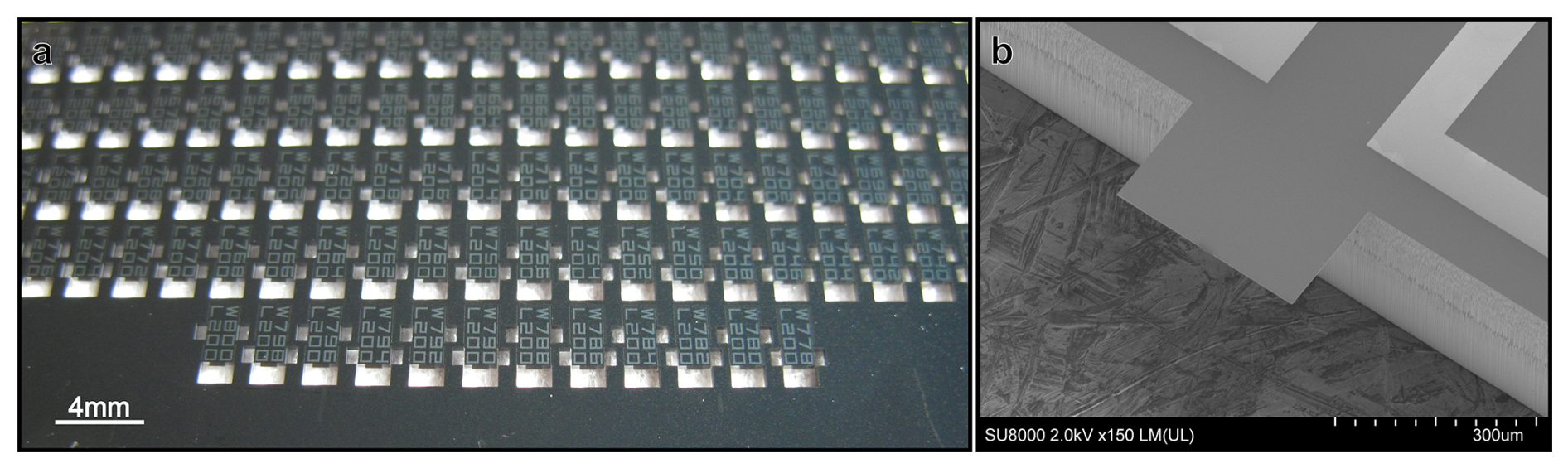
Figure 1(a) Optical micrograph of single-side clamped plate-shaped MEMS resonators with different geometries. Every device is labeled according to its width (W) and length (L) in micrometers. (b) SEM image of a 330 µm wide and 200 µm long resonator.
The devices are actuated photo-thermally using a ThorLabs laser diode with a wavelength of 635 nm and a typical optical output power of 2.5 mW (model LPS-635-FC). The mechanical response of the resonator is measured optically with a Micro System Analyzer (MSA) 500 from Polytec GmbH with a vertical scanning head and an adjustable measurement laser with a wavelength of 633 nm. The scanning head is equipped with a bright field objective with a zoom factor of 10 and a corresponding field of view of 0.9 mm × 0.67 mm. Additionally, to the measurement laser, the optical fiber of the actuation laser diode is mechanically integrated into the scanning head of the MSA, making a precise manual adjustment of the actuation position possible. After converting the optical signal to an electrical signal in the vibrometer controller of the MSA, the internal MSA signal analyzer or an external lock-in amplifier (Zurich Instruments HF2LI) is used to process the data. The external lock-in amplifier increases the flexibility of the setup as well as the measurement precision.
MEMS device characterization is performed under vacuum conditions to avoid dominating gas damping. A Pfeiffer rotary vane pump (DUO 3 M) is placed below the table and connected to the chamber with a flexible tube (inner diameter 25 mm). For quality factor determination, pressure levels of about mbar ensure that gas damping has less impact, as reported by Schiwietz et al. (2023), and Kulygin et al. (2008).
3.1 Measurement setup
The measurement setup schematically shown in Fig. 2 and as a photograph in Fig. 3 consists of several key elements described subsequently. The LDV scanning head and an XYZ stage are mounted to the same vibration-damped table. The XYZ stage is assembled from a vertical (X-VSR20A) and two horizontal (X-LSM100A and X-LSM150A) stages by Zaber, controlled via a script due to a serial connection to a PC. Mounted to the X stage, a custom-built vacuum chamber can be positioned very precisely below the scanning head of the LDV setup. The vacuum chamber is designed to fit wafers with a diameter of 100 mm or smaller snippets and is sealed with a coated glass window optimized for low reflectance in the range of 425 to 675 nm. Four ports in the vacuum chamber ensure reliable connections of the vacuum pump, pressure gauge, and electrical connections, respectively. The electrical signal is processed by the vibrometer controller of the MSA and analyzed by either the internal MSA signal analyzer or an external lock-in amplifier. Furthermore, the driving frequency and amplitude of the actuation laser can be adjusted with both the MSA signal generator and the lock-in amplifier.
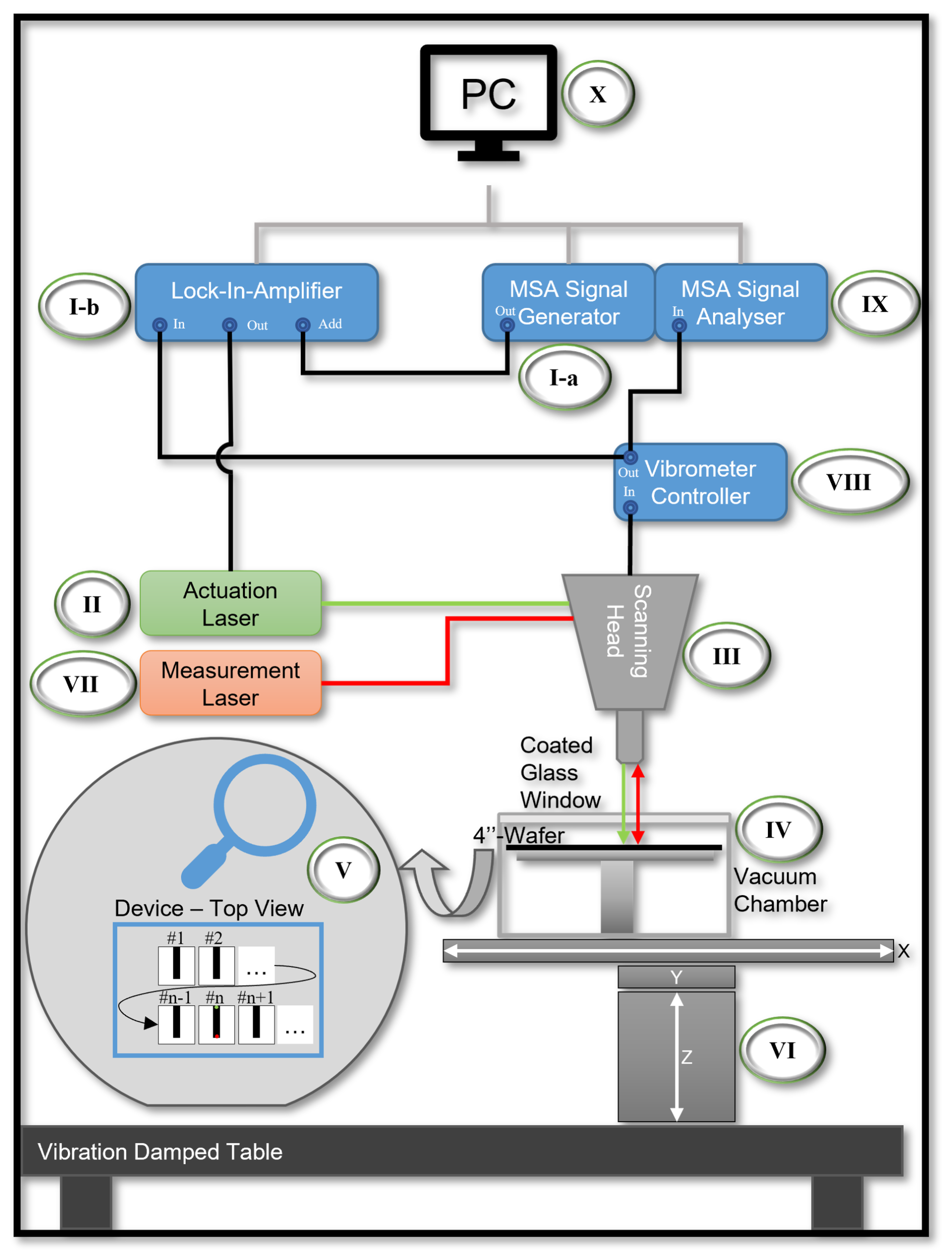
Figure 2Schematic of the LDV measurement setup. The labeled parts follow the information processing, starting at the MSA signal generator (I-a) and the lock-in amplifier (I-b), generating the driving signal for the actuation laser (II). The fiber of the diode laser is mechanically integrated into the scanning head (III) so that the light goes through the lens, and the coated glass window goes into the vacuum chamber (IV) and actuates the DuT (V). The positioning of the device below the microscope is performed with the XYZ stage (VI). Furthermore, the response characteristics of each resonator are measured using the measurement laser (VII) and processed by the vibrometer controller (VIII). Detailed analysis of the resonance properties of the device is performed by the MSA signal analyzer (IX) and the lock-in amplifier (I-b), both connected to a PC (X).
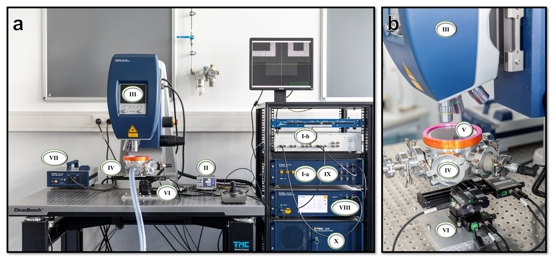
Figure 3Photographs of the tailored, LDV-based measurement setup from different view angles in panels (a) and (b). The components labeled with Latin numbers from I to X are described in the caption of Fig. 2.
The workflow is illustrated in Fig. 4, starting from the fabrication of MEMS resonator devices with out-of-plane resonance modes (A1) via the placing of the wafer in the vacuum chamber (A2) with the additional needed pre-adjustment of the microscope settings (A3) and the setup of the reference coordinate system, including the number of devices to be measured (A4). Subsequently, to these manual steps, the algorithm proceeds for every device of interest by automatically performing a rough lateral positioning (B1) followed by the auto-focus (B2) and the contour detection of the actual resonator geometry (B3). This enables the exact positioning of the resonator anchor region relative to the position of the actuation laser (B4) and, consequently, the exact positioning of the measurement laser at the location of interest. Since plate resonators show a high amplitude at the corners of the resonator independent of the out-of-plane eigenfrequency, the measurement laser is moved to one of the corners to start the wide-band frequency measurement (B5). Next, a peak detection is performed in the measured frequency spectrum (B6). If resonance peaks are found, the algorithm changes the control of the actuation laser to the lock-in amplifier, enabling a precise narrow-band frequency sweep around the corresponding peak frequency (C1) from which the mode-specific quality factor is extracted by fitting a Lorentzian function to the data. Optionally, scan points can be defined across the resonator (D1), and an area scan can be performed (D2).
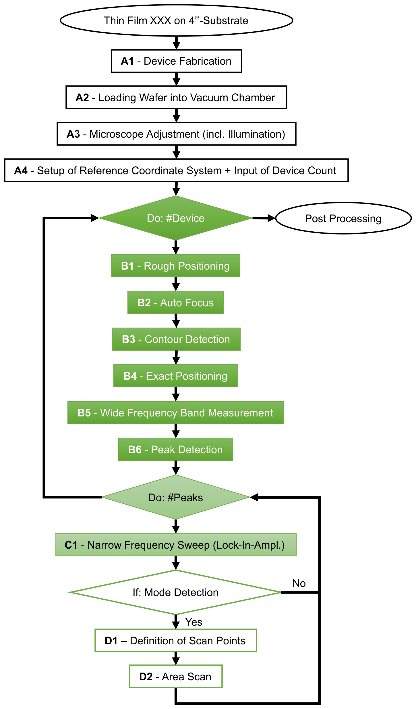
Figure 4Process flow for the analysis of MEMS resonator devices with respect to out-of-plane resonance modes. The devices are fabricated from a thin film of interest (A1) at the wafer level. Subsequently, the wafer must be loaded into the vacuum chamber (A2), and the microscope needs to be adjusted (A3). Before starting an automated measurement cycle, the user must set up a reference coordinate system and choose the number of devices measured (A4). The algorithm performs a loop for the number of devices with the following steps: rough positioning – auto focus – contour detection – exact positioning – wide frequency band measurement – peak detection (B1–B6). For every found peak, a narrow-band frequency sweep is performed using a lock-in amplifier (C1), and if activated, scan points on the resonator are defined, and an area scan for the mode shape analysis is performed (D1 and D2).
The position of the resonators is precisely known from the design of the lithography mask. Nevertheless, several steps are needed to get a sharp microscope image of the resonator in the correct position for the photo-thermal actuation. First, the system moves to the resonator position laterally on the wafer, according to the mask design (rough positioning B1). Anyhow, related to imperfections in the resonator fabrication, stress in the thin film, or tolerances in the stage movement, the resonator might not be in the focal point, and the correct lateral position might be off by up to tens of micrometers, as shown in Fig. 5a. Second, an auto-focusing step (B2), as illustrated in Fig. 5b, is performed to get the maximal signal level of the LDV detector and sharp resonator edges to perform the final exact positioning (B4) of the resonator relative to the actuation laser. This feedback loop leads to the precise positioning of each individual device under the microscope of the MSA scanning head and an accurate photo-thermal actuation within a few micrometers, as shown in Fig. 5c. The exact positioning is done with contour detection (B3) by an image recognition tool. Hence, the position of the measurement laser can be set close to the corner of the resonator, also with micrometer accuracy. Subsequently, wide-band frequency measurements (B5) are performed, containing the resonance modes of interest. An example measurement is shown in Fig. 6. The data show a range from 50 to 500 kHz and are the basis for the decision regarding whether a found peak corresponds to an actual resonance mode or originates from parasitic environmental impact from different sources such as thermal noise, vibrational sources such as vacuum pumps, or electromagnetic sources from other labor equipment.
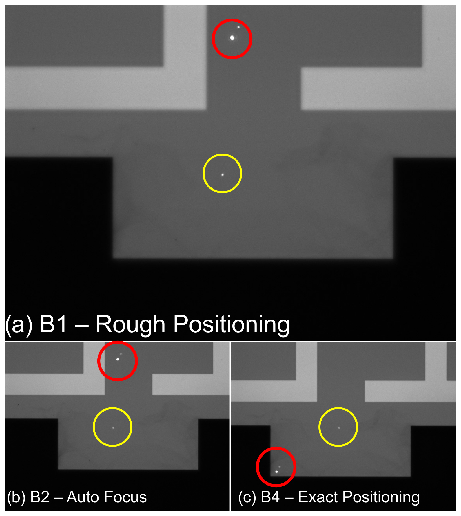
Figure 5Plate resonators with different geometries are placed in a regular grid with an x distance of 2450 µm and a y distance of 4400 µm. This information is used for the rough positioning step in panel (a). Subsequently, the auto-focus procedure is performed using the signal level of the measurement laser as a reference. Therefore, the laser spot is placed in the substrate region of the device to avoid problems with broken resonators (red circle). The sharp device contour in panel (b) is necessary for the contour detection algorithm, which provides the information on the plate size and the position of the corners to do the exact positioning for the actuation laser (yellow circle) in panel (c). Overall, the travel range from one device to the start of the measurement on the next device takes 10 to 15 s depending on the bow of the wafer and the corresponding movement in the z direction.
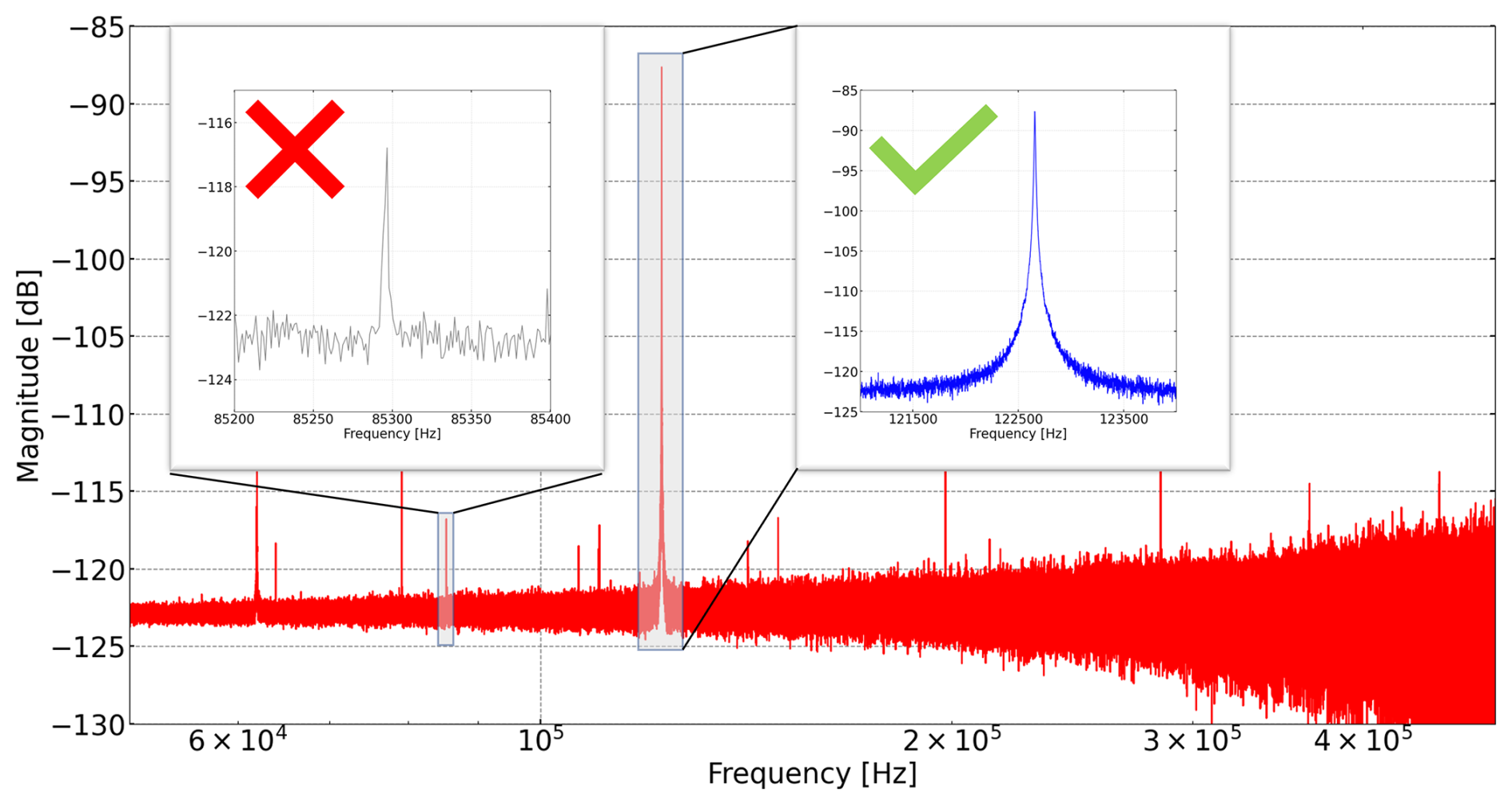
Figure 6The frequency band from 40 to 540 kHz of a 800 µm wide and 200 µm long resonator contains several visible peaks, which can be resonance peaks (green tick) or perturbations from different sources such as thermal noise, vibrational sources such as vacuum pumps, or electromagnetic sources from further labor equipment (red cross). The algorithm in Fig. 4 (B6) makes decisions based on the peak height and peak width at half maximum if the found peak is stored and used for the subsequent steps.
If a found peak is determined to be a resonance mode (B6), due to a threshold value of the peak height above the noise level and a minimum peak width of more than 1 Hz at half maximum, the algorithm switches the drive of the actuation laser from the MSA signal generator (I-a) to the lock-in amplifier (I-b) to perform a narrow-band frequency sweep (C1). Three examples of this measurement performed with the lock-in amplifier are shown in Fig. 7. Since the quality factor of a resonance mode is a device parameter of utmost importance, it is extracted from the resonance curve by fitting a Lorentzian function. The used fitting curve related to the transfer function X(f) of the driven, damped harmonic oscillator is multiplied with the frequency f in Eq. (1) to allow for a fitting procedure of the measured data in the velocity domain (V(f) = fX(f)).
The fitting parameters are a constant offset C, the amplitude A, the center frequency of the peak f0, and the quality factor Q. The resonance curve in Fig. 7a is an example of a frequency response, which can be fitted in high accordance with the function in Eq. (1). Even though another resonator with the same geometry is measured for the resonance curve in Fig. 7b, there is a difference in the peak frequency of 59 %. This drastic change cannot be explained by variations in the resonator height due to uncertainties in the device layer thickness and thus exceeds the calculated frequency range for the device geometry, which is also discussed below in Fig. 9. Rather, this result shows that the described setup can be used to spot devices on the wafer with divergent properties. Finally, the Lorentzian fitting cannot lead to conversion for every resonator's frequency response, as shown in Fig. 7c. In further studies, resonance curves with this specific shape can be investigated to gather new insights into the field of nonlinear features in MEMS devices. There are several possible causes for such a vibrational response of the resonator, including not only geometric nonlinearity, nonlinear damping, and inertial nonlinearity (see Lifshitz and Cross, 2008), but also intermodal coupling, causing internal resonances (see Asadi et al., 2018). In the scope of this work, resonance curves with this behavior are excluded from further analysis of the quality factor. Optionally, area scans at the found resonance frequency can be performed within the algorithm by choosing a specific bandwidth. The scan points for the area scan use the information from the contour detection (B3), and the number of points in x and y directions can be chosen. The overall measurement time per resonance mode on a single device, including peak detection, frequency sweep, and grid scan is in the range of 1 min depending on the necessary filter settings of the lock-in amplifier and the chosen number of grid scans for mode identification.
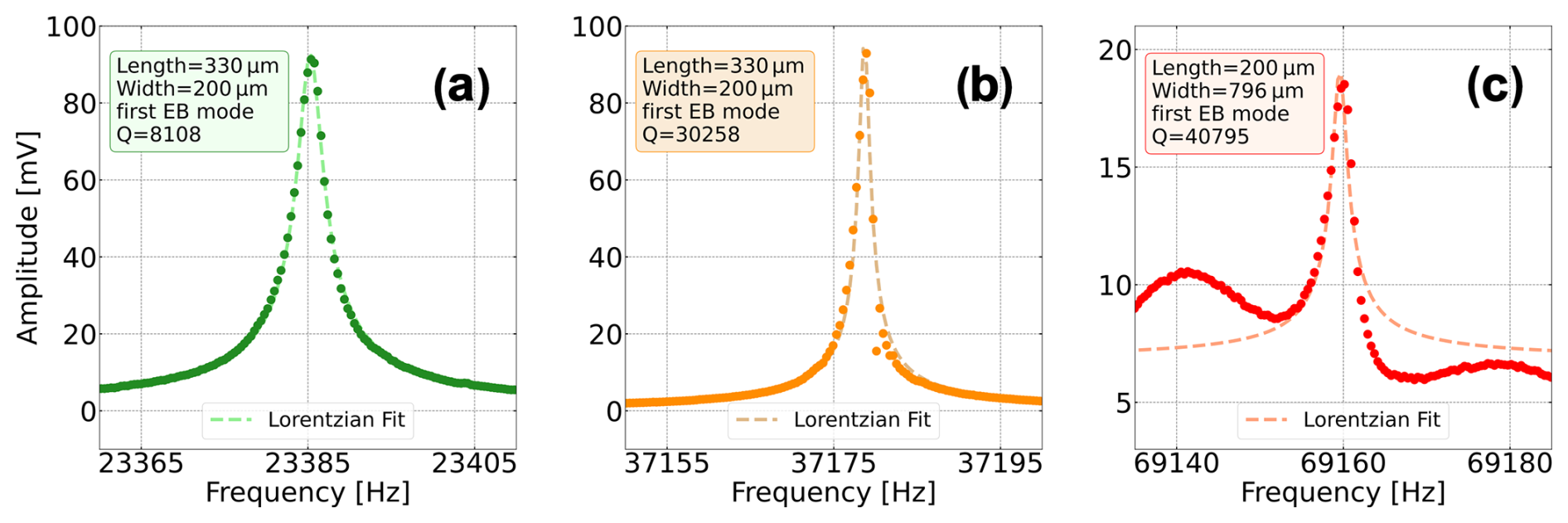
Figure 7Typical resonance curves of the first Euler–Bernoulli mode of SCSi plate resonators measured with a lock-in amplifier (C1) under vacuum conditions (about mbar). In panel (a) an example of a fit in high accordance with the Lorentzian function is shown. For panel (b), a resonator with the same dimensions as in panel (a) leads to a difference in the peak frequency of 59 %. This can be used to detect devices out of tolerance. The measured resonator in panel (c) shows nonlinear behavior, and the Lorentzian fitting does not converge. The measured resonance curves (dots) are fitted with a Lorentzian function (dashed line) to determine the quality factor.
3.2 Analysis of resonance frequency and quality factor
Figure 8 demonstrates the results of the automated measurement of 460 devices fabricated on one SOI wafer. The gained data of the first Euler–Bernoulli mode are shown as squares (resonance frequency) and circles (quality factor), while unmeasured DuTs are marked with a red X. In some cases, the resonance frequency is measured correctly, while the quality factor cannot be extracted from the resonance curve due to nonlinearities in the devices (see Fig. 7c). For these devices, the circles representing the quality factor are also replaced with a red X. Across the wafer, there are areas that show a certain tendency toward lower or higher resonance frequency. Due to the constant length of the devices, this behavior shows that even small deviations in the thickness of the SCSi thin film can be displayed with this technique since the resonance frequency is proportional to the height of the device. Quality factors do not follow the same trends but seem to change more randomly from device to device, which may arise from the fabrication process of the device layer as well as the devices, where, e.g., contaminants on the surface can affect the quality factor. For example, the eighth device in the sixth row shows extraordinarily high resonance frequency and quality factor values, which is also shown in Fig. 7b. The microscope image inserted in Fig. 8 reveals contamination on the resonator surface, which causes deviation from the expected result.
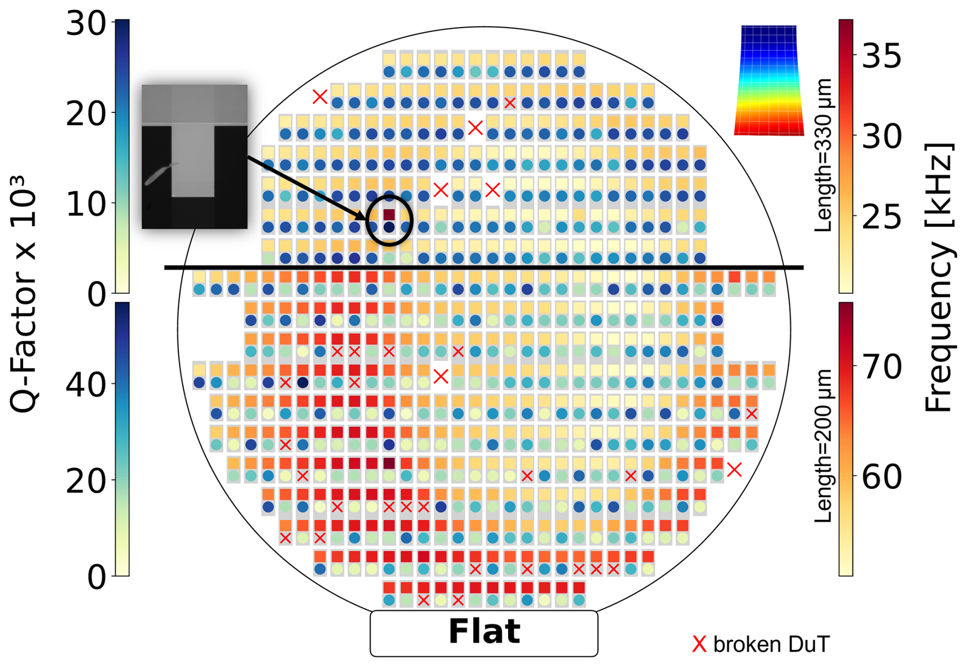
Figure 8The LDV measurement of the first Euler–Bernoulli mode of all devices on a wafer is shown. As presented in Fig. 5, the devices on the wafer are single-side clamped plate-shaped silicon resonators. The wafer is separated into the upper area (above the black line) with devices with a length of 330 µm and the lower area (below the black line) with devices with a length of 200 µm. For every device on the wafer, the resonance frequency and the quality factor are shown as squares and circles, respectively. Unmeasured DuTs are marked with a red X. The different areas have separate color bars as the resonance frequency depends on the resonator length.
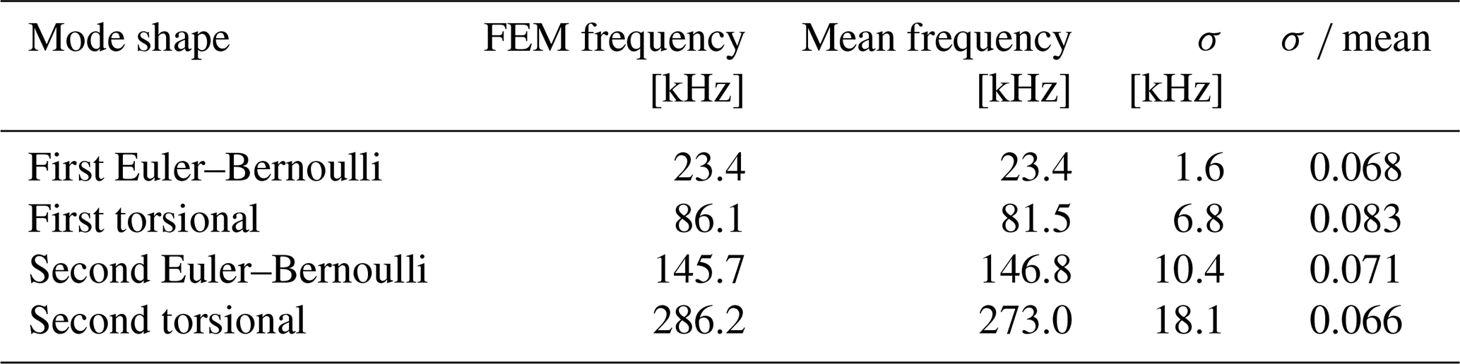
Further measurements of other out-of-plane resonance modes are performed within the same measurement run, where wide bandwidth measurements for the devices also show higher-order modes according to the resonator geometry. With increasing frequency from 20 up to 320 kHz, four modes are found, as shown in Fig. 9. The order of the modes for the 330 µm long and 200 µm wide plate resonators and the corresponding mean resonance frequencies are summarized in Table 1. The ratio of standard deviation over mean resonance frequency is constant for all modes, giving additional indication on the presence of local device layer thickness variations. A finite-element method (FEM) simulation of a 330 µm long and 200 µm wide SCSi plate resonator using COMSOL Multiphysics shows good agreement with the measured mean resonance frequencies as the first four eigenmodes are calculated from a FEM simulation for the device with a thickness of 1.8 µm and reported in Table 1. In addition, the blue hatched area in Fig. 9 highlights the frequency range calculated by a sweep of the device thickness in the FEM simulation from 1.5 to 2.1 µm, hence within the tolerance range stated by the wafer manufacturer. Overall, the measured quality factor in the range from 10 000 to 80 000 is expected for SCSi MEMS resonators, as has been reported in the literature for decades (e.g., Bienstman et al., 1996; Nguyen and Howe, 1999; Cioffi and Wan-Thai, 2005; Kulygin et al., 2008). Despite this agreement, the scatter diagrams of the modes look different. The data for the first and second Euler–Bernoulli modes seem to be uniformly distributed. In contrast, the first and second torsional modes show a linear trend of increasing quality factor with resonance frequency. Accordingly, due to this result and the large difference in the mean quality factor, the modes are expected to experience different dominant loss mechanisms. Thermoelastic dissipation (TED) is the possible reason for the reduced quality factor of the Euler–Bernoulli modes since Chandorkar et al. (2009) state that TED is negligible for pure torsional modes due to the reduced mechanical deformation of the resonator.
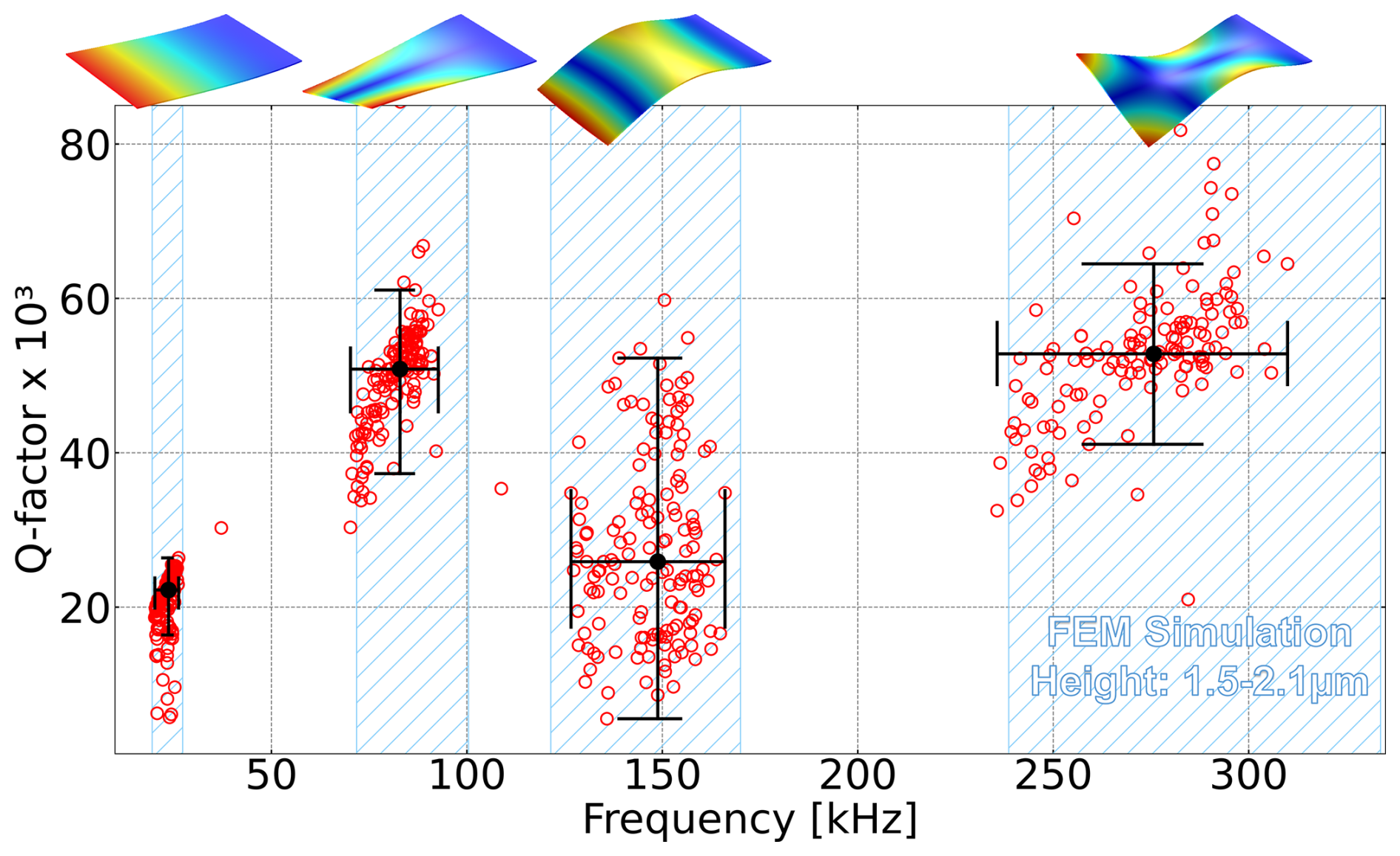
Figure 9A detailed study of 160 devices, in the upper area of the wafer discussed in Fig. 8 in the frequency band ranging from 20 to 320 kHz, shows four different resonance modes. The plate-shaped resonators with a length of 330 µm, a width of 200 µm, and a height of 2 ± 0.5 µm are measured under vacuum at a pressure level of about mbar. The blue hatched area highlights the frequency range calculated by FEM simulations when sweeping the device thickness from 1.5 to 2.1 µm.
Table 1Order of the modes and corresponding eigenfrequencies calculated with FEM simulations for a mean thickness of 1.8 µm and the measured mean frequency for 160 devices.
A tailored measurement setup to monitor variations of device geometries, as well as material properties, has been developed, allowing for the collection of the frequency-dependent response characteristics of many devices time-efficiently for statistical analysis. In contrast to solutions where the LDV measurement head is mounted to a semi-automatic probe station described in Gennat et al. (2013) and available on the market, the actuation is performed without contact as a diode laser is used to actuate the devices photo-thermally. The conducted single-point LDV measurements are done to identify resonances and extract quality factors from Lorentzian fits. In doing so, any electrical wiring is avoided for an early-stage characterization during the fabrication process flow. The devices are measured under vacuum conditions of about mbar in a custom-built vacuum chamber.
The presented setup is a powerful tool for studying many devices during the design process of new MEMS devices and for research applications. Here, the large number of measurement points enables a profound statistical analysis, thus strengthening the scientific statements and giving insights into the physical phenomena of each DuT.
With the described setup, it is possible to study a large variety of device geometries since different bright field objectives can be used with the scanning head. The range of supported objectives from Polytec GmbH ranges from a zoom factor of 1 with the corresponding field of view of 9 mm × 6.7 mm and a laser spot diameter of < 55 µm to a zoom factor of 100 with a corresponding field of view of 0.09 mm × 0.067 mm and a laser spot diameter of < 1 µm. A limiting factor is the actuation power of the diode laser effectively transferred to the DuT and available to drive the resonance mode. This is especially relevant for the described wide-band frequency measurements, where the laser power is split into all actuated frequencies. To increase the power density per measured frequency, the wide frequency band is split into several bands and measured incrementally. With this approach, the measurement time increases, but the size of measurable device dimensions can also be increased.
The measurement setup will be used for prospective studies as MEMS resonators with out-of-plane resonance modes are of broad interest in semiconductor research and industry. Different device designs can be studied concerning loss mechanisms and nonlinear effects in the resonator. These gained insights can lead to improvements in MEMS resonator design for new applications and further miniaturization. In addition, the described setup shows high potential to study the influence of coatings, surface, and material treatments on the vibrational properties of MEMS resonator devices. In the future, studying different device geometries might also lead to the identification of interesting devices for the investigation of all kinds of linear and nonlinear intermodal coupling effects. However, it will make it necessary to improve the vacuum system for devices more affected by fluid damping due to the remaining pressure in the vacuum chamber. For that purpose, a turbomolecular pump can be used next to the chamber connected via a vacuum tube, or a lightweight model can be mounted to the chamber. To improve the cost efficiency of the presented system, the measurement time could be further reduced by performing ring-down measurements for the extraction of the quality factor instead of narrow-band frequency sweeps. Furthermore, basic single-point laser Doppler vibrometers without an adjustable measurement laser can be used when the whole device positioning process is performed with the XYZ stage, or an approach with position-sensitive detectors (PSDs) instead of LDV could be an option.
The used computer code is available on request from the corresponding author (dominik.huber@tuwien.ac.at).
The data that support the findings of this study are available from the corresponding author upon reasonable request (dominik.huber@tuwien.ac.at).
The conceptualization of the paper was done by DH, GP, and US. DH prepared the original draft, while GP and US supervised. MS contributed with resources and built the software together with DH and PF. GP acquired the funding for the project and did the administration. Infrastructure and other resources were contributed by US. Finally, investigations and visualizations were performed by DH.
At least one of the (co-)authors is a member of the editorial board of Journal of Sensors and Sensor Systems. The peer-review process was guided by an independent editor, and the authors also have no other competing interests to declare.
Publisher's note: Copernicus Publications remains neutral with regard to jurisdictional claims made in the text, published maps, institutional affiliations, or any other geographical representation in this paper. While Copernicus Publications makes every effort to include appropriate place names, the final responsibility lies with the authors.
The authors gratefully acknowledge the financial support from the Österreichische Forschungsförderungsgesellschaft (FFG) through the RESONANCE project (project no. 888041).
This research has been supported by the Österreichische Forschungsförderungsgesellschaft (grant no. 888041).
This paper was edited by Michele Penza and reviewed by two anonymous referees.
Algamili, A. S., Khir, M. H. M., Dennis, J. O., Ahmed, A. Y., Alabsi, S. S., Ba Hashwan, S. S., and Junaid, M. M.: A Review of Actuation and Sensing Mechanisms in MEMS-Based Sensor Devices, Nanoscale Res. Lett., 16, 16, https://doi.org/10.1186/s11671-021-03481-7, 2021. a
Asadi, K., Yu, J., and Cho, H.: Nonlinear couplings and energy transfers in micro- and nano-mechanical resonators: intermodal coupling, internal resonance and synchronization, Philos. T. Roy. Soc. A, 376, 20170141, https://doi.org/10.1098/rsta.2017.0141, 2018. a
Bienstman, J., Tilmans, H. A. C., Peeters, E. J. E. A., Steyaert, M., and Puers, R.: An oscillator circuit for electrostatically driven silicon-based one-port resonators, Sensor. Actuat. A.-Phys., 52, 179–186, https://doi.org/10.1016/0924-4247(96)80146-4, 1996. a
Chandorkar, S. A., Candler, R. N., Duwel, A., Melamud, R., Agarwal, M., Goodson, K. E., and Kenny, T. W.: Multimode thermoelastic dissipation, J. Appl. Phys., 105, 043505, https://doi.org/10.1063/1.3072682, 2009. a
Cioffi, K. R. and Wan-Thai, H.: 32KHz MEMS-based oscillator for low-power applications, in: Proceedings of the 2005 IEEE International Frequency Control Symposium and Exposition, Vancouver, BC, 29–31 August 2005, IEEE, 551–558, https://doi.org/10.1109/FREQ.2005.1573992, 2005. a
Clark, J. R., Hsu, W. T., Abdelmoneum, M. A., and Nguyen, C. T. C.: High-Q UHF micromechanical radial-contour mode disk resonators, J. Microelectromech. S., 14, 1298–1310, https://doi.org/10.1109/JMEMS.2005.856675, 2005. a
Duane, S. B. and James, E. C.: Statistical metrology: understanding spatial variation in semiconductor manufacturing, in: Proc. SPIE 2874, Microelectronic Manufacturing Yield, Reliability, and Failure Analysis II, Austin, TX, United States, 16–18 October 1996, SPIE, 2874, 16–26, https://doi.org/10.1117/12.250817, 1996. a
Gaidarzhy, A., Imboden, M., Mohanty, P., Rankin, J., and Sheldon, B. W.: High quality factor gigahertz frequencies in nanomechanical diamond resonators, Appl. Phys. Lett., 91, 203503, https://doi.org/10.1063/1.2804573, 2007. a
Gennat, M., Meinig, M., Shaporin, A., Kurth, S., Rembe, C., and Tibken, B.: Determination of Parameters With Uncertainties for Quality Control in MEMS Fabrication, J. Microelectromech. S., 22, 613–624, https://doi.org/10.1109/JMEMS.2012.2236076, 2013. a, b
Kulygin, A., Schmid, U., and Seidel, H.: Characterization of a novel micromachined gyroscope under varying ambient pressure conditions, Sensor. Actuat. A-Phys., 145–146, 52–58, https://doi.org/10.1016/j.sna.2007.10.088, 2008. a, b
Kurth, S., Mehner, J., Shaporin, A., Michael, S., Ebert, M., Dötzel, W., and Gessner, T.: Determination of dimensional parameters in MEMS components by vibration analyses, in: Structural dynamics; IMAC XXV, Conference Proceedings of the Society for Experimental Mechanics Series, Florida, USA, 19–22 February 2007, Society for Experimental Mechanics, 165–235, ISBN: 0912053968, 2007. a
Lifshitz, R. and Cross, M. C.: Nonlinear Dynamics of Nanomechanical and Micromechanical Resonators, in: Reviews of Nonlinear Dynamics and Complexity, edited by: Schuster, H. G., John Wiley & Sons, Ltd, Chap. 1, 1–52, https://doi.org/10.1002/9783527626359.ch1, 2008. a
Nguyen, C. T. and Howe, R. T.: An integrated CMOS micromechanical resonator high-Q oscillator, IEEE J. Solid-St. Circ., 34, 440–455, https://doi.org/10.1109/4.753677, 1999. a
Pfusterschmied, G., Kucera, M., Steindl, W., Manzaneque, T., Ruiz Díez, V., Bittner, A., Schneider, M., Sánchez-Rojas, J. L., and Schmid, U.: Roof tile-shaped modes in quasi free–free supported piezoelectric microplate resonators in high viscous fluids, Sensor. Actuat. B-Chem., 237, 999–1006, https://doi.org/10.1016/j.snb.2016.02.029, 2016. a
Pfusterschmied, G., Patocka, F., Weinmann, C., Schneider, M., Platz, D., and Schmid, U.: Responsivity and sensitivity of piezoelectric MEMS resonators at higher order modes in liquids, Sensor. Actuat. A-Phys., 295, 84–92, https://doi.org/10.1016/j.sna.2019.05.031, 2019. a
Pfusterschmied, G., Weinmann, C., Schneider, M., Platz, D., Shen, N., Sader, J., and Schmid, U.: Sound dissipation from plate-type resonators excited in non-conventional transversal modes in liquids, J. Micromech. Microeng., 30, 075004, https://doi.org/10.1088/1361-6439/ab8bc9, 2020. a
Rothberg, S. J., Allen, M. S., Castellini, P., Di Maio, D., Dirckx, J. J. J., Ewins, D. J., Halkon, B. J., Muyshondt, P., Paone, N., Ryan, T., Steger, H., Tomasini, E. P., Vanlanduit, S., and Vignola, J. F.: An international review of laser Doppler vibrometry: Making light work of vibration measurement, Opt. Laser. Eng., 99, 11–22, https://doi.org/10.1016/j.optlaseng.2016.10.023, 2017. a
Schiwietz, D., Weig, E. M., and Degenfeld-Schonburg, P.: Thermoelastic damping in MEMS gyroscopes at high frequencies, Microsystems & Nanoengineering, 9, 11, https://doi.org/10.1038/s41378-022-00480-1, 2023. a
Tao, Y., Boss, J. M., Moores, B. A., and Degen, C. L.: Single-crystal diamond nanomechanical resonators with quality factors exceeding one million, Nature Communications, 5, 3638, https://doi.org/10.1038/ncomms4638, 2014. a