the Creative Commons Attribution 4.0 License.
the Creative Commons Attribution 4.0 License.
 | 30 Oct 2018
Magnetic-field CMOS microsensor for low-energy electric discharge detection
Mohamed Hadj Said
Farès Tounsi
Libor Rufer
Hatem Trabelsi
Brahim Mezghani
Andrea Cavallini
This paper addresses the development and characterization of a non-intrusive silicon-based microsensor, which can detect electric partial discharges in electrical insulation equipment. Early partial discharge detection prevents failures and can be used to optimize maintenance operations. Despite the potential that CMOS technology offers, miniaturized electric discharge detector has neither been investigated nor implemented, until now. The developed microsensor demonstrates its ability to record electric discharge emission thanks to the presence of a miniaturized planar inductor. The squared inductor of 50 turns with a side length of 1.5 mm used in our sensor has been fabricated on top of a silicon substrate in a CMOS technology. The total inductor wire length of loop antenna is 30 cm to achieve 100 MHz bandwidth. Using the microsensor at 1 cm from the discharge site, a damped sinusoidal induced voltage with an amplitude of 2 V has been measured at its output. We observed that the output signal spectrum is highly concentrated around a central resonance frequency, which remains constant. The main advantage of such design resides in its monolithic integration added to the high autonomy, which improves the microsensor efficiency.
- Article
(1906 KB) - Full-text XML
- BibTeX
- EndNote


When the electric field across an insulator exceeds the dielectric strength, an electric discharge (ED) occurs. The discharge is called partial when it does not short-circuit the whole insulation (Montanari, 2016). Depending on the features of the discharge site, partial discharge (PD) can be divided into four types: internal discharge, corona discharge, surface discharge, tracking and treeing discharges (Thi, 2011; Kreuger et al., 1993). The electric discharge phenomenon causes a progressive degradation of the properties of the surrounding material under the action of electron bombardment and chemical erosion. Indeed, various phenomena can be triggered by a PD, such as thermal stress locally generated by the discharge. Under high voltages, this stress can cause chalking and carbonization of the insulation causing the degradation of the insulating material. In addition, it leads to chemical attack due to degradation products generated by the discharge (ozone, nitrogen oxides and nitric acid in particular). When the insulation degradation becomes critical, a full arc occurs between two phases or between phase and ground causing a total breakdown of the insulation (Yaacobi et al., 2014). Detection of electric discharges at an early stage greatly helps in avoiding system failures and allows the optimization of any required maintenance procedure. Our work focuses on the development of a novel generation of integrated electric discharge detector, fabricated using standard industrial complementary metal oxide semiconductor (CMOS) process. This paper demonstrates the proof of concept of an electric discharge detection technique using a miniaturized CMOS-based planar inductor. This method exploits electromagnetic radiation emissions, in the form of radio frequency waves, which mark discharge phenomena in high-voltage cables, as an example. A sensing part based on the electromagnetic induction is common in traditional sensors having the size of units to tens of millimeters. However, it can be considered as emerging when using CMOS-based technology (Robles et al., 2008; Rozi and Khayam, 2015). The main advantage of the proposed sensor is its size, which eases deployment in the field. The feasibility of the proposed method was validated by laboratory measurements and characterizations. Important differences between the proposed sensor and other electromagnetic-based sensors result from the fabrication process. In our case, the sensor can be strongly miniaturized by using an industrial CMOS technology. In addition, the proposed inductive microsensor is battery-free and low-cost if produced in a batch process. Moreover, it can be integrated very closely to high-voltage equipment and can send the information to a distant monitoring system. The CMOS technology allows the co-integration of mixed digital–analog circuitry with the sensing inductor, which can increase the performance and decrease noise due to the reduction of interconnection parasitic capacitance. The most important advantage of miniaturization is the fact that it can be placed as close as possible to known weak spots in the insulation. This will certainly improve the detection sensitivity compared with sensors placed at larger distances. In this paper, we will present the design, measurement setup, and preliminary characterization results of this novel on-chip monolithic inductive electric discharge sensor. The ultimate target is the deployment of a distributed sensor network for monitoring PD in distribution power grids. Therefore, this work aims only at demonstrating the capability of a CMOS-compatible microsensor to detect electrical discharges occurring in electrical insulation equipment.
Over the past four decades, several methods have been developed to detect the presence of complete and partial breakdown mechanisms in dielectrics. These can be grouped into four categories: chemical, optical, acoustic, or electrical techniques. Indeed, when a discharge occurs, there is a chemical change in the material due to hot electrons in the avalanche which can decompose the surrounding materials into different chemical components. Thus, a gas analyzer could be exploited to detect its presence (Yaacobi et al., 2014; Zhou et al., 2016). Optical methods are used as well since the light emitted due to ED/PD is generally in the UV–visible range. Acoustically, the pulse created by a discharge is in the ultrasonic range (Horstink, 2014; Kunicki et al., 2016). At 10 cm distance, the acoustic pressure from a 1 pC discharge is about 0.2 Pa and from a 10 pC discharge source is 0.6 Pa (Lopez-Higuera, 2002). Piezoelectric acoustic sensors such as the Harisonic G-0504 and PAC R15I-AST are often used to detect and locate PD in power transformers because of their high sensitivity in the range of hundreds of kilohertz (Guide for industrial ultrasonic). Using MEMS technology and fiber optics, an acousto-optical PD sensor using the Fabry–Pérot interferometer has been developed (Posada-Roman et al., 2012; Wang et al., 2005).
Various electrical methods were developed to detect PD phenomena. Indeed, electrical detection with high-frequency current transformer sensor (HFCT), also called radio frequency current transducer (RFCT), is widely used. The HFCT sensor consists of an induction coil with a ferrite core suitable for the measurement of transient signals in the range of tens of megahertz. These pulses can have a rise time of few nanoseconds, corresponding to a frequency spectrum with significant components up to hundreds of megahertz or even units of gigahertz (Yaacobi et al., 2014; Wang et al., 2016). HFCT sensors are easy to design, manufacture, and are inexpensive for commercialization. In fact, they might suffer from electromagnetic interference and be vulnerable to noise.
The ultra-high-frequency (UHF) method is alternatively used to detect the electromagnetic signals associated with the PDs. In fact, by using UHF antennas or an inductive probe in proximity of possible defect sites, the electromagnetic wave can be detected. The frequency band of electromagnetic PD signals is usually from hundreds of megahertz to several gigahertz, which allows avoiding effectively low-frequency noise and interferences. The electric component of the electromagnetic wave can be detected by a capacitive sensor, which corresponds to a patch antenna or microstrip antenna (Ghani and Chakrabarty, 2008; Álvarez et al., 2015; Shibuya et al., 2010). Also, the magnetic component of the electromagnetic wave can be detected using an inductive probe. When time-varying magnetic field is passing through a coil, it induces a voltage across its terminals. To maximize this induced voltage, a resonant loop sensor is designed. For PD sensor requiring flat frequency response, a wideband induction coil is designed instead, to be able to detect PD-induced EM waves in a given frequency range. Numerous types of coil inductors such as circular, square, etc. with 100 MHz bandwidth are reported in Rozi and Khayam (2015; Fig. 1). It was proved that the sensitivity of the circle loop antenna was the best among the other designs, because it can reach 120 mV at 5 cm above the PD source (Rozi and Khayam, 2015). An inductive rectangular loop in macroscopic scale designed on a 12 cm × 0.9 cm area circuit board is documented in Robles et al. (2008). In the measurement setup using an applied voltage of 2.4 kV to the dielectric, a voltage of 2 V was measured at the loop output. Another millimetric-scale sensor with a single-layer air-core probe of 5 turns, 3 mm length, and 1.3 mm coil radius, having the sensitivity of about 40 mA m−1, and the time response of 0.8 ns in the frequency range from 200 MHz to 1 GHz was designed and reported in Wang et al. (2016). The inductor output was around 19 mV at a distance of 12 cm from the discharge source. The magnetic field of around 0.48 A m−1 was measured in this configuration. To the best of our knowledge, there are no publications related to the magnetic PD detection using both CMOS and MEMS technologies.

Figure 1Inductive coils designed for magnetic partial discharge detection: (a) triangular shape and (b) rectangular shape (Rozi and Khayam, 2015).
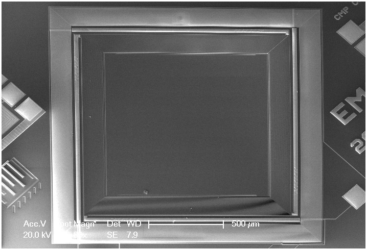
This work aims to test the capability of a CMOS-compatible microsensor to detect electrical discharges that generally occur in electrical insulation equipments. The sensing part consists mainly of an on-chip planar inductor allowing the exploitation of the magnetic field associated with an ED emission and subsequently to assess the severity of the defect affecting an insulation system. The proposed method is efficient and suitable for measurement, but it also has issues like low immunity to the electromagnetic interference and to noise. These problems can be solved by using a suitable band-pass filter and by selecting carefully the inductor resonance frequency (Álvarez et al., 2015). Another limitation leads in the need of several inductive sensors to detect the electrical discharge location by analyzing the arrival times of corresponding pulses (time-of-flight measurements) and, finally, obtaining the ED location. Because of its simple layout and symmetry, a square spiral inductor is used. Our approach focuses on low-cost CMOS manufacturing obtained by processing chips issued from an industrial standard CMOS process. In this approach, we use silicon and other layers issued from a CMOS process as base materials for the system structure. The SEM picture of the tested structure of the CMOS-based electrical discharge detector is shown in Fig. 2. The dimensions of the planar inductor, which is designed to form the structure of the ED detector, are given in Table 1. The latter is a prototype fabricated using standard CMOS technology 0.6 µm (2P2M) provided by the foundry CSMC (ICC – Integrated Circuit Center design, China). The equivalent π-model circuit of the planar inductor is detailed in Jenei and Bart (2002) and Yue and Wong (2000). The total dimensions of the fabricated chip are 3 mm × 3 mm × 0.7 mm (Fig. 2). The inductance value calculated with the Greenhouse method is estimated to be around 22 µH with a serial resistance of about 17 kΩ (Jenei and Bart, 2002).
According to Faraday's law, the phenomenon of electromagnetic induction occurs once there is a magnetic flux time variation through an inductor coil. This induced voltage is called transformer induction (emft), and it depends on the time variation of the magnetic B-field through the considered closed loop surface and is defined by Tounsi et al. (2009):
where S is the surface element based on the contour of the closed spiral inductor oriented in the same direction as the B-field emitted by the outbreak of the ED. Therefore, the sensor is sensitive to the B-component, which is oriented only in the same direction as the surface S. The inductance plays the role of a planar multi-turn loop antenna. To achieve a high sensitivity, its dimensions must be optimized. The relationship between frequency (f), wavelength (λ), and the speed of light (c) is given by . Therefore, the total length of the wire forming the inductance was set to be 10 times of a wavelength for the valid uniform-current approximation (Werner, 1996). Since the square looped inductor is designed to detect ED-induced EM wave in air with frequency up to 500 MHz, the total wire length of this loop antenna is set to be approximately 30 cm ( µm) to achieve 100 MHz bandwidth.
To be able to test the CMOS inductor, we have built a simple circuit to generate low-energy electrical discharge, which is shown in Fig. 3 (Banerjee et al., 2013). Because ED magnitude is quite low (in the order of pC), and the sensing inductor dimensions and quality factor have not been optimized yet, a simple electric discharge trigger has been preferred over other designs. The discharge generating circuit is composed of a resistor, capacitor, spark electrodes with a gap and a low voltage excitation source. Indicatively, the electric discharge intensity can be set by the energy stored in the capacitor. In addition, the use of the resistor in the circuit helps in producing a constant type discharge and to limit the intensity of the current generated by the voltage source. When the applied voltage reaches a sufficiently high value, the air around the electrodes is ionized and an electron avalanche will cross the gap, eventually establishing an arc. If the discharge occurs between the bare electrodes (as in this case), the energy stored in the circuit will be discharged through the arc, with a time constant that depends on the internal resistance and self-inductance of the faulted component and of all components in the circuit. In an insulating system, the discharge can destroy the insulation and generate a full electric spark. In this case, the discharge is called as total. If a dielectric barrier stops the avalanche, the discharge will extinguish, and the system will continue to operate. In this case, a partial discharge occurs.
Concerning the spark gap system, when the distance between electrodes increases, the breakdown voltage increases as well. The discharge is accompanied with an emission of acoustic and electromagnetic energy. When varying the distance between the source and the sensor, we can estimate its sensitivity limit for an electric discharge. In this discharge gap, the maximum voltage applicable will be established by the Paschen curve. This curve provides different breakdown voltages in air for different distances between both electrodes. The Paschen curve can be described by the breakdown voltage as given in Koliatene et al. (2008):
where VB (V) is the breakdown voltage, p (Pa) is the pressure, d (m) is the gap distance, γ is the secondary electron emission coefficient at the cathode (Townsend coefficient), A is the saturation ionization in the gas at a particular E∕p (electric field / pressure), and B is related to the excitation and ionization energies. The constants A and B are determined experimentally and found to be roughly constant over a restricted range of E∕p for any given gas (Sili, 2012). In ambient conditions, the breakdown electric field in the air between two parallel plates is around 3.6 kV mm−1 (Sili, 2012).

To properly choose the value of breakdown voltage, we need to know the minimum of the Paschen curve in air under ambient conditions. For that, we also need to identify the secondary coefficient of Townsend γ, which is an important parameter since it depends on the material properties and on the form of the electrodes. When the Townsend coefficient is very high, the minimum of Paschen curve decreases as mentioned in Koliatene et al. (2008) and Sili (2012). Therefore, in the tested circuit, a DC voltage source V0 of 150 V is used to charge the capacitor C1 (1 µF), through a resistor R1 (200 kΩ) to adjust the charging current. For the used voltage, the gap distance is found to be 4.5 µm.
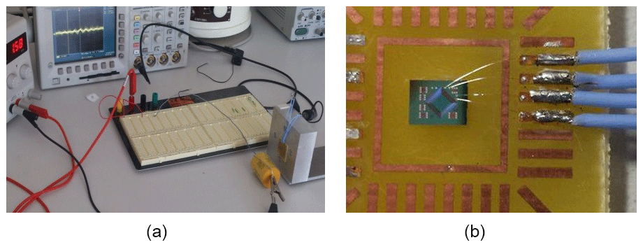
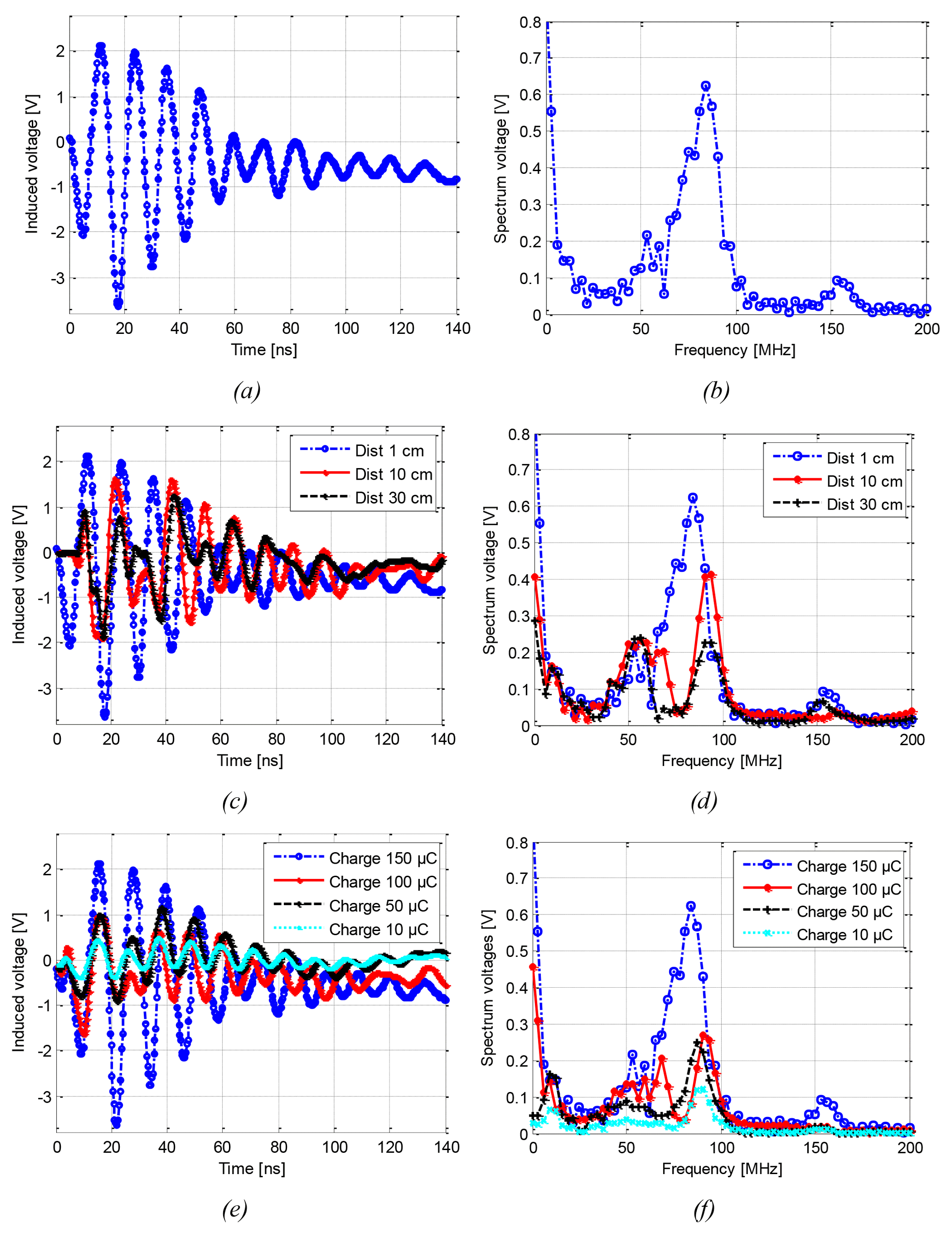
Figure 5Microsensor (a) induced output voltage over time, (b) spectrum of the signal in case (a), (c) induced output voltage over time for different separation distances, for applied voltage of 150 V, (d) spectrum of signals in case (c), (e) induced voltage output over time for various released charges, for 1 cm separation from source, (f) spectrum of signals in (e).
Initially, the chip with the sensor was mounted on a PCB containing pads, which are connected to the inductor by wire bonding using ultrasonic welding (Fig. 4b). According to the Faraday's law, an induced voltage is generated at the microsensor terminals each time an electric discharge gives rise to a time-varying magnetic field. The characterization of the discharge-sensor-induced voltage was performed in a simple arrangement allowing a discharge generation. To this end, the capacitor was charged using the DC generator. Next, the voltage source was disconnected and the distance between capacitor terminals was reduced progressively. In this way, a spark discharge was generated when reaching a point-to-point gap indicated by Paschen curve. This arrangement simulates discharges resulted from the dumping of stored energy in any system capacitors to the components of the system, leading to the component damages. Simultaneously, the output voltage waveform due to the magnetic energy detected was recorded for further processing and comparison. Experimentally, the sensor was fixed to an aluminum support facing the capacitor, at an initial distance of 1 cm, which was charged up to 150 µC. The sensor terminals were connected to a Keysight digital sampling oscilloscope DSO-X 2014A having a bandwidth of 100 MHz and a sampling rate of 2 GSa s−1, and it can record the signal emitted by the discharge system using simple logic trigger. Figure 5a shows the induced voltage waveform captured by the magnetic probe, obtained from the experiment shown in Fig. 3. The inductor records a sinusoidal damped signal with first peak amplitude around 2 V, and total discharge duration equal to 150 ns before fading away. The fast Fourier transform (FFT) signal spectrum of the discharge signal recorded is given in Fig. 5b showing a peak around the central frequency of 84.38 MHz. Indeed, the small loop sensor is useful for receiving the UHF signal, so it must be designed to maximize the induced voltage for certain resonance frequency (self-inductor resonance). In Rozi and Khayam (2015), the sensor was designed to be resonant at frequency around 100 MHz. In Ghani and Chakrabarty (2008), the loop inductor was designed to be resonant at frequency between 200 MHz and 1 GHz. The theoretical pulse current generated within the circuit, upon a breakdown, has duration of around few nanoseconds (Cooper et al., 1984; Tomita, 2008). Thus, its spectrum should have a bandwidth up to 500 MHz. On the other hand, the ideal sensor bandwidth should cover frequencies up to 100 MHz to detect the frequency emitted by the discharge. But, since the sensor is resonant around a certain frequency, the output signal will be maximal around this same resonant frequency (Ganjovi, 2016). A similar form of a damped signal, due to an electrical spark discharge, was documented in Martinson and Delsing (2010) and Liu et al. (2015).
In Fig. 5c results of the experiment are plotted showing the sensor output voltage obtained when varying the distance between the electric discharge source and the sensor itself. The corresponding spectrums are represented in Fig. 5d. It can be noted that the measured signal magnitude is inversely proportional to the separation distance. It is also worth noting that the spectrum peak frequency remains almost the same for tested distances above 10 cm (see Fig. 5b). Therefore, from the microsensor frequency response in Fig. 5d, it can be noted that the device exhibits a higher sensitivity when used in the vicinity of a given resonant frequency (Ganjovi, 2016). Thus, for a specific application, we should optimize the sensor geometry in order to match the frequency range where electric discharge energy prevails noise. Moreover, Fig. 5e shows the relation between the discharge energy and the sensor output signal. We can note, as well, that the signal amplitude decreases as the applied voltage decreases. This corresponds to a decrease of the induced current and also of the radiated magnetic wave. Here again, the spectrum shows a peak around the same frequency for different input voltages since the sensor is resonant around a critical frequency so the output signal will be maximal around this same resonant frequency. Thus, as a perspective to this work, we need to optimize the dimensions of our inductor structure in order to increase the sensor bandwidth. Our experiments resulted in an estimation that the studied silicon-based miniaturized microsensor is sensitive to low electric discharges with capacitor charge around 10 µC.
In this preliminary work, we demonstrate the CMOS-based sensor capability to detect the magnetic field associated with electric partial discharges through experimental results. Although the energy released by the electron avalanche is low, it is sufficient to degrade the dielectric during time, leading to breakdown. The proposed sensor paves the way to implement a non-intrusive detection technique suitable to build sensor networks. So far, very few attempts have been made to develop such integrated sensor. In our investigation, a spark generator circuit to trigger the electric discharge has been employed to generate a damped sinusoidal output voltage. Separation distances varying from 1 up to 30 cm were investigated. As well, by varying the released charge, we were able to detect the presence of the EM released by the spark gap. It is worth noting that the recorded discharge signals have no significant components at frequencies above 100 MHz. This work represents a proof of concept concerning the possibility of using an integrated CMOS-based microsensor to detect the electric discharge presence. Future works will investigate the inductor parameters' influence on the obtained induced voltage and the means to improve the microsensor sensitivity.
Please contact the corresponding author for further discussion of the published data.
The authors declare that they have no conflict of interest.
This work was carried out with support provided by the Tunisian Ministry
of Higher Education and Scientific Research in the framework of the
Programme des Jeunes Enseignants-Chercheurs (PJEC) in the field of
engineering science (grant ref: 18PJEC12-16).
Edited by: Michael Kraft
Reviewed by: three anonymous referees
Álvarez, F., Garnacho, F., Ortego, J., and Sánchez-Urán, M. Á.: Application of HFCT and UHF Sensors in on-Line Partial Discharge Measurements for Insulation Diagnosis of High Voltage Equipment, Sensors-Basel, 15, 7360–7387, 2015.
Banerjee, S., Deb, A. K., Rajan, R. N., and Kishore, N. K.: Detection of Electrical Discharges in DC Accelerator Using Photomultiplier Tubes, in: 1st IEEE International Conference on Condition Assessment Techniques in Electrical Systems, 6–8 December 2013, Kolkata, India, 2013.
Cooper, J. A., Dewhurst, R. J., Moody, S., and Palmer, S. B.: High-voltage spark discharge source as an ultrasonic generator, IEEE Proc. A, 131, 275–281, 1984.
Ganjovi, A.: A parametric study on the PD pulses activity within micro-cavities, J. Theor. Appli. Phys., 10, 61–74, 2016.
Ghani, A. B. A. and Chakrabarty, C. K.: The detection of magnetic field from Partial Discharge (PD) signal in XLPE cable using inductive probe, in: Proceedings of International Symposium on Electrical Insulating Materials, 7–11 September 2008, Yokkaichi, Mie, Japan, 2008.
Horstink, R.: How Ultrasound Can Detect Electrical Discharge Non-invasively and Help Eliminate Arc Flash Incidents, in: 11th International Conference on Live Maintenance (ICOUM'14), 21–23 May 2014, Budapest, Hungary, 2014.
Jenei, S. and Bart, K. J. C.: Physics-based closed-form inductance expression for compact modeling of integrated spiral inductors, IEEE J. Solid-St. Circ., 37, 77–80, 2002.
Koliatene, F., Lebey, T., Cambronne, J. P., and Dinculescu, S.: Impact of the aeronautic environment on the Partial Discharges Ignition: A basic study, in: IEEE International Symposium on Electrical Insulation, July 2008, Vancouver, Canada, 2008.
Kreuger, F. H., Gulski, E., and Krivda, A.: Classification of partial discharges, IEEE T. Dielect. El. In., 28, 917–931, 1993.
Kunicki, M., Cichoń, A., and Borucki, S.: Study on Descriptors of Acoustic Emission Signals Generated by Partial Discharges under Laboratory Conditions and in On-Site Electrical Power Transformer, Arch. Acoust., 41, 265–276, 2016.
Liu, J., Zhang, G., Dong, J., and Wang, J.: Study on Miniaturized UHF Antennas for Partial Discharge Detection in High-Voltage Electrical Equipment, Sensors-Basel, 15, 29434–29451, 2015.
Lopez-Higuera, J. M.: Handbook of Optical Fiber Sensing Technology Part 4 – Applications, John Wiley, Chichester, UK, 2002.
Martinson, E. and Delsing, J.: Electric spark discharge as an ultrasonic generator in flow measurement situations, Flow Meas. Instrum., 21, 394–401, 2010.
Montanari, G. C.: Partial discharge detection in medium voltage and high voltage cables: maximum distance for detection, length of cable, and some answers, IEEE Electr. Insul. M., 32, 41–46, 2016.
Posada-Roman, J., Garcia-Souto, J. A., and Rubio-Serrano, J.: Fiber Optic Sensor for Acoustic Detection of Partial Discharges in Oil-Paper Insulated Electrical Systems, Sensors-Basel, 12, 4793–4802, 2012.
Robles, G., Manuel-Martínez, J., Rojas, M., and Sanz, J.: Inductively coupled probe for the measurement of partial discharges, Rev. Sci. Instrum., 79, 055104, https://doi.org/10.1063/1.2924207, 2008.
Rozi, F. and Khayam, U.: Development of Loop Antennas for Partial Discharge Detection, Int. J. Elect. Eng. Inform., 7, 29–41, 2015.
Shibuya, Y., Matsumoto, S., Tanaka, M., Muto, H., and Kaneda, Y.: Electromagnetic Waves from Partial Discharges and their Detection using Patch Antenna, IEEE T. Dielect. El. In., 17, 862–871, 2010.
Sili, E.: Etude et caractérisation des décharges partielles et du vieillissement du polyimide en environnement aéronautique, PhD Thesis, Toulouse University, Toulouse, France, December 2012.
Thi, A. T. V.: Propriétés diélectriques de matériaux isolants sous contraintes impulsionelle répétitive: Application aux modules de commutation en électronique de puissance, PhD Thesis, University of Grenoble Alpes, Grenoble, France, 2011.
Tomita, H.: Effect of charge in the time of charging voltage on spark discharge from a metal disk, IEEE J. Trans. Fundament. Mater., 128, 577–584, 2008.
Tounsi, F., Mezghani, B., Rufer, L., Mir, S., and Masmoudi, M.: Electromagnetic modeling of an integrated micromachined inductive microphone, in: 4th IEEE International Conference on Design & Technology of Integrated Systems in Nanoscal Era, 6–9 April 2009, Cairo, Egypt, 2009.
Wang, S., Hu, H., Wang, W., Li, F., Yan, X., Wang, Y., and Wang, L.: Design of UHF-SHF Sensor for the Detection of GIS Partial Discharge, in: Electrical Insulation Conference (EIC), 19–22 June 2016, Montréal, Canada, 2016.
Wang, X., Li, B., Xiao, Z., Hwui-Lee, S., Roman, H., Russo, O. L., Chin, K. K., and Farmer, K. R: An ultra-sensitive optical MEMS sensor for partial discharge detection, J. Micromech. Microeng., 15, 521–527, 2005.
Werner, H.: An Exact Integration Procedure for Vector Potentials of Thin Circular Loop Antennas, IEEE T. Antenn. Propag., 44, 157–165, 1996.
Yaacobi, M. M., Alsaedi, M. A., Rashed, J. R., Dakhil, A. M., and Atyah, S. F.: Review on Partial Discharge Detection Techniques Related to High Voltage Power Equipment Using Different Sensors, Photonic. Sensors, 4, 325–337, 2014.
Yue, C. P. and Wong, S. S.: Physical Modeling of Spiral Inductors on Silicon, IEEE T. Electron Dev., 47, 560–568, 2000.
Zhou, W., Zheng, Y., Yang, S., Li, H., Wang, B., and Qiao, S.: Detection of intense partial discharge of epoxy insulation in SF6 insulated equipment using carbonyl sulfide, IEEE T. Dielect. El. In., 23, 2942–2948, 2016.