the Creative Commons Attribution 4.0 License.
the Creative Commons Attribution 4.0 License.
 | 09 Aug 2022
Fabrication of integrated polysilicon waveguides for mid-infrared absorption sensing
Gerald Stocker
Cristina Consani
Pooja Thakkar
Clement Fleury
Andreas Tortschanoff
Khaoula-Farah Ourak
Gerald Pühringer
Reyhaneh Jannesari
Parviz Saeidi
Elmar Aschauer
Ulf Bartl
Christoph Kovatsch
Thomas Grille
Bernhard Jakoby
The increasing popularity of environments equipped with sensors for convenience and with safety features, as in, for example, smart homes, greenhouses, or the interior of modern cars, demands a variety of sensor systems. In this respect, the sensing of ambient gases in the sense of air quality monitoring or leakage detection is one of the prominent applications. However, even though there are many different systems already available, the trend goes towards smaller and rather inconspicuous sensors which are embedded in the environment. We present the fabrication and characterization of integrated waveguides, which constitute an interesting platform for absorption spectroscopy in the mid-infrared (mid-IR) using the evanescent field of guided modes interacting with the analyte, thus leading to the absorption-induced attenuation of the mode. Corresponding simulations, characterizing the efficiency of the desired interaction, predict values for the confinement factor Γ and the intrinsic damping D for a waveguide geometry, which is then characterized by measurements. Furthermore, we discuss how these waveguides could be part of an integrated, non-dispersive, mid-IR sensor system fully integrated on a single chip. In this context, we present a way to maintain the quality of waveguides throughout the entire workflow needed to integrate a pyroelectric IR detector based on aluminum nitride (AlN).
- Article
(6234 KB) - Full-text XML
- BibTeX
- EndNote


The advances in the development of sensor-controlled environments over the past decade have fueled the demand for a wide variety of sensor systems able to perform environmental sensing. In this context, micro-fabricated sensors are especially of great interest, as many applications allow only a small footprint. Talking about ambient gas monitoring, the market provides different solutions based on photo-acoustic (PAS) or non-dispersive infrared (NDIR) sensing, with both still facing the challenge of being miniaturized (Eberl et al., 2019; Ranacher et al., 2019; Ng et al., 2021; Lavchiev and Jakoby, 2017).
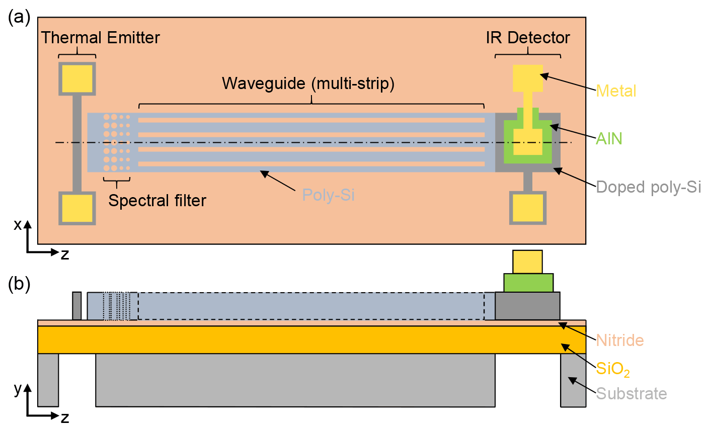
Figure 1Schematic of an integrated, non-dispersive mid-infrared (NDIR) sensor system. (a) Top view of the system, depicting a thermal emitter, a spectral filter, a multi-strip waveguide, and an infrared (IR) detector. (b) Cross section through the dash-dotted line shown in panel (a).
In order to tackle this challenge, we aim to develop a monolithic, fully integrated NDIR sensor system for on-chip gas measurements. A schematic of the envisioned sensor system is shown in Fig. 1. The system's key components are a thermal emitter, as source of radiation, a spectral filter for wavelength selectivity (central wavelength of 4.24 µm), a waveguide as the area of interaction between the guided radiation and the ambient atmosphere, and a detector for mid-IR radiation. In the given schematic, a phosphorus-doped polysilicon wire equipped with metal pads forms the thermal emitter. The pyroelectric IR detector shown is composed of doped polysilicon, aluminum nitride (AlN), and a metal layer (Ranacher et al., 2019). In order to reduce the thermal capacitance of the emitter and detector part, the silicon substrate is removed underneath these structures. A polysilicon waveguide between the emitter and detector ensures that the radiation can be guided along a controllable path (Ranacher et al., 2018b). Since the evanescent field of the waveguide is used for the interaction between the guided radiation and the surrounding gas, the waveguide length influences the reachable detection limit. Meander-shaped waveguides can increase the effective path length and therefore lower the detection limit without changing the footprint of the sensor too much. In this context, the waveguide geometry needs to be optimized such that coupling losses and intrinsic damping are as low as possible (Consani et al., 2018). Besides this tradeoff, the described waveguide concept allows a rather easy integration of a spectral filter, which allows us to determine the wavelengths guided (Němec et al., 2005; Jannesari et al., 2017; Costa et al., 2003).
In this work, we present the fabrication of integrated polysilicon waveguide structures and their characterization with respect to the damping behavior and confinement factor. The discussed multi-strip waveguide concept is derived from former work by our group, in which we already investigated the idea of using a single-slot waveguide, designed for IR radiation, for gas sensing purposes (Ranacher et al., 2018a). The advantage of this array of coupled strips is that the coupling between waveguides pushes the electric field stronger in the gaps between the structures, as compared to an isolated strip, thus increasing the amount of field usable for the sensing and, finally, the efficiency. Additionally, having multiple waveguides allows for higher light throughput, and thus higher sensitivity to smaller concentrations can be achieved. Moreover, we discuss the involved processes during the micro-fabrication of the envisioned sensor system which have a negative impact on the waveguide quality. In particular, we present ways to maintain the waveguide quality throughout the employed process flow. Thereby, the entire fabrication is performed on 8 in. (= 200 mm) silicon substrates (wafers) in the industrial clean room facilities of Infineon Technologies Austria AG.
Details concerning the fabrication are provided in Sect. 3, followed by the description of the damping measurements in Sect. 3. The negative impact of subsequent dry-etching processes during fabrication on the waveguide structures is discussed in Sect. 4. This section also covers possible solutions to the problems described.
Preliminary results of this work were presented at the MikroSystemTechnik Kongress 2021 and published in its proceedings (Stocker et al., 2021). This extended paper provides further and deeper insights to the study and the experiments carried out.
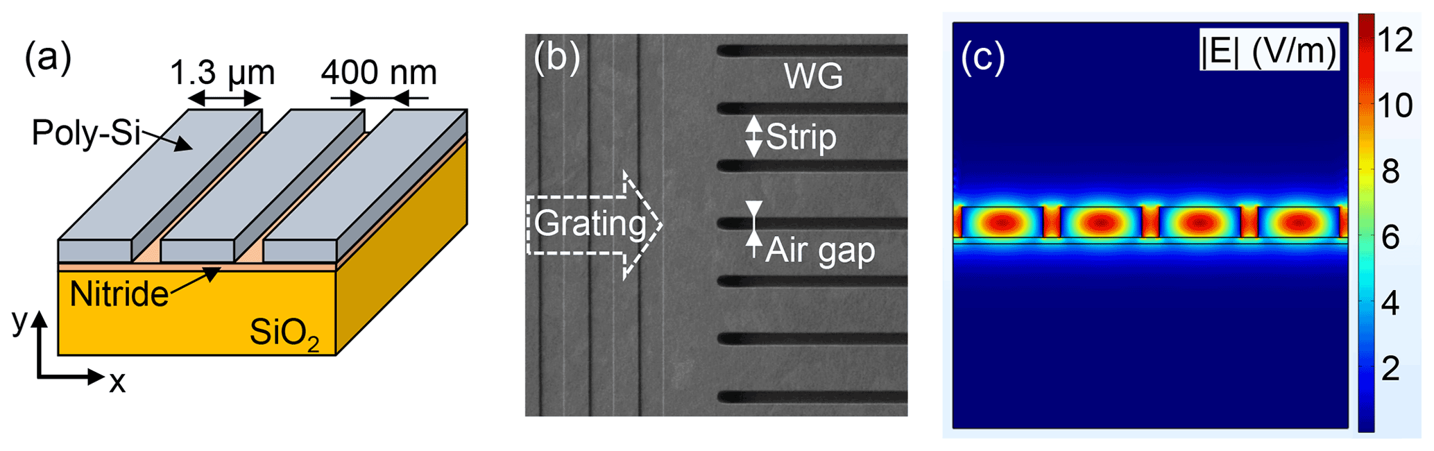
Figure 2The proposed multi-strip waveguide structure as platform for evanescent field sensing. (a) Schematic of a multi-strip waveguide structure. (b) Scanning electron microscope (SEM) image of the fabricated waveguide. The waveguide is equipped with a coupler grating on the left (top view without tilt). (c) Simulated field distribution () for the lowest-order TE mode, revealing the evanescent field to be mainly present in the air gaps. Finite element method (FEM) simulation carried out in COMSOL Multiphysics® software.
The fabrication of the described waveguide structures is performed on 8 in. (= 200 mm) silicon substrates, which constitute a standard wafer diameter within the clean room facilities at Infineon Technologies Austria AG. The performed micro-fabrication employs a wide range of processes which are state of the art in the semiconductor industry and well explained in the literature (see, e.g., Cordes et al., 2010). As a first step in the fabrication, a system plane made of silicon oxide (SiO2; 2 µm) and silicon nitride (Si3N4; 140 nm) is deposited on the substrate. This system plane is thought to act as a kind of insulating layer to decouple the waveguide from the substrate. The electric field of the guided modes should not leak into the silicon substrate underneath. Therefore, this insulating layer helps to decrease the intrinsic damping of the waveguide. On top of the system plane, the bulk material for the actual waveguide, emitter, and detector is deposited, namely 660 nm of undoped polysilicon (Poly-Si), combining a standard chemical vapor deposition (CVD) process to deposit the silicon in an amorphous state and a temperature treatment at around 900 ∘C to bring the silicon into an polycrystalline state. In order to structure this layer and to form the individual components of the sensor system, a combination of photolithography (spin coating, exposure, and developing) and dry etching is performed. What follows is an implantation step which changes the electric conductivity of the polysilicon at the emitter and detector region. After this implantation, the AlN layer is deposited and structured, which is explained in Sect. 4. Finally, a metallic layer is deposited to cover the AlN and the contact pads at the emitter and detector to enable the wire bonding necessary for emitter steering and detector readout. A schematic of a resulting waveguide structure is shown in Fig. 2, together with a scanning electron microscope (SEM) image of the corresponding fabricated structure. The dimensions of the shown waveguide structure are a strip width of 1.3 µm and a gap width of 0.4 µm. The SEM image also reveals a coupler grating located next to the multi-strip waveguide. This grating allows light to be coupled in from an external source into the waveguide, which is needed to perform damping measurements on the waveguide structures (see Sect. 3). The corresponding simulation of the electric field distribution () of the lowest-order TE (transverse electric) mode is shown in Fig. 2c. The finite element method (FEM) simulation, carried out in COMSOL Multiphysics® software, reveals the presence of the evanescent field mainly in the air gaps of the multi-strip waveguide.
From these simulations, we derived the chosen geometry for the fabricated and characterized waveguide structure, namely a strip width/gap width of µm. According to simulations, this structure provides an confinement factor of around Γsim=16 % and a intrinsic damping of the order of Dsim=0.5 cm−1.
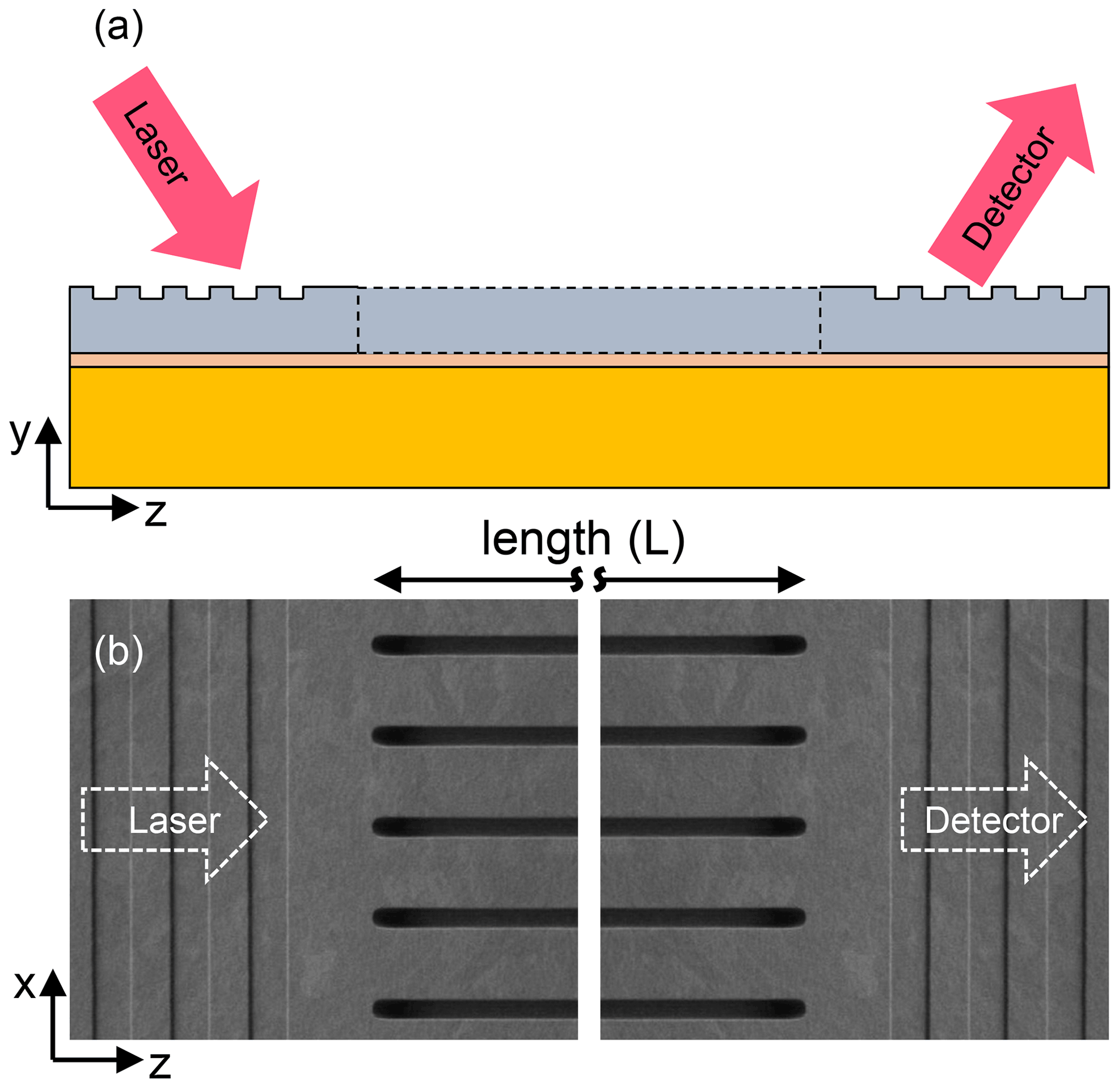
Figure 3Concept and corresponding test structures to determine the waveguide damping. (a) Schematic representation of the performed damping measurement. Light from an external laser is coupled in via a grating, transmitted through the waveguide, and coupled out towards an external detector. (b) Stitched SEM image of a fabricated test structure (top view without tilt).
In order to quantify the quality of the fabricated waveguides with respect to intrinsic damping, the structures are equipped with coupler gratings. As shown in Fig. 3a and b, the gratings are located at the beginning and the end of the waveguide. Light from an external laser source (4.24 µm wavelength) is coupled in the waveguide, transmitted, and coupled out again. The transmitted intensity is thereby determined by an external detector. According to the Beer–Lambert model, the ratio of the transmitted intensity Iout and the initially introduced intensity from the laser source Iin is proportional to an exponentially decreasing function, as follows:
where L and D are the length and the damping value of the investigated waveguide structure, respectively. A series of measurements consists of three measurements performed on structures of the same geometry but of a different length (1.25, 2.5, and 5 mm). The damping value is determined as the slope of a linear fit, which is performed after plotting the measured data of the transmitted intensity on a logarithmic scale. Figure 4 reveals the results measured for the described waveguide geometry (strip/gap width of µm). The measured values are subject to the coupling efficiency, which is affected by the grating quality and fiber alignment. The fiber alignment is stable over the measurement of three waveguides (three lengths) on the same chip as the stage carrying the wafer can be used, but it can vary, as we need to move the wafer manually to access another chip. Therefore, the slope is stable (single chip measurement) over the measurement, but a chip-to-chip variation is perceptible in the data.
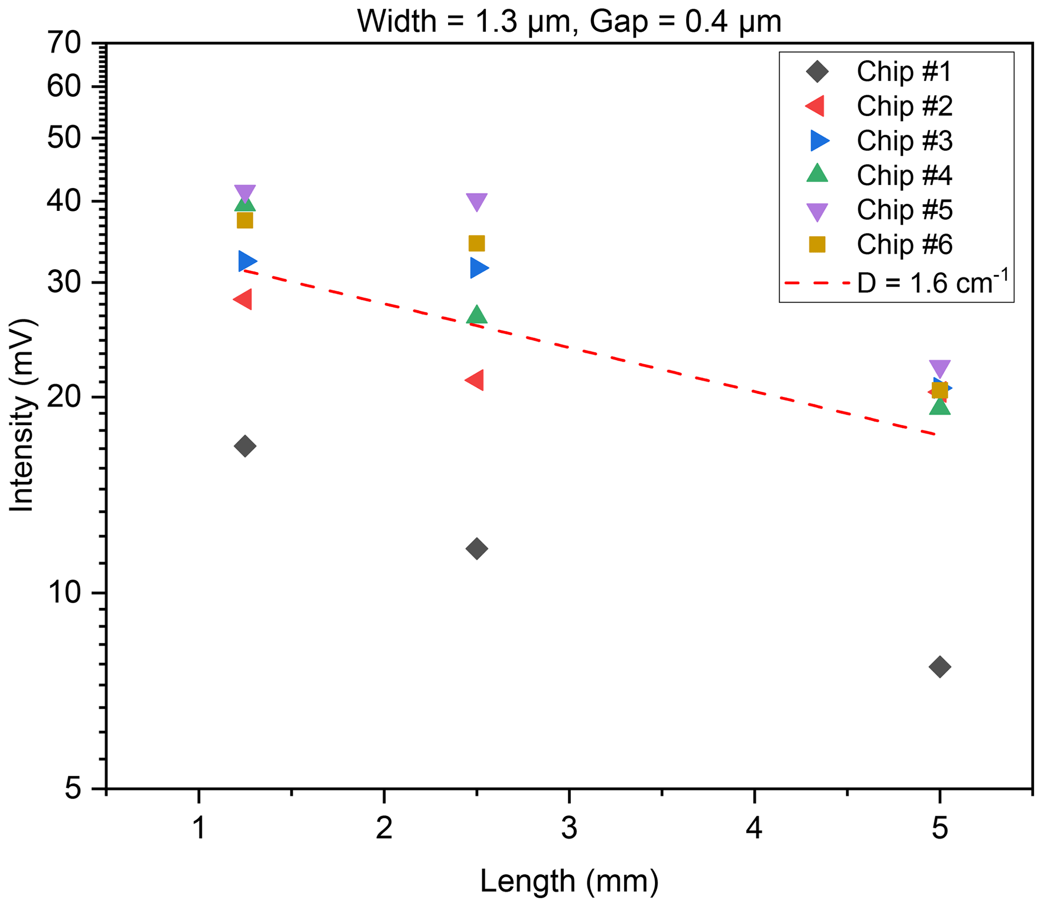
Figure 4Determination of waveguide damping. The measured intensity of transmitted light through multi-strip waveguides of three different lengths (L=1.25, 2.5, and 5 mm) is plotted on a logarithmic scale. The damping is determined by an linear fit (red dashed line). For the described waveguide geometry (width = 1.3 µm/gap = 0.4 µm), a damping value of Dexp=1.6 cm−1 is found.
The value for intrinsic damping is found to be around Dexp=1.6 cm−1, which is roughly 3 times higher than predicted by simulations. The discrepancy between the simulated and the experimental damping value has two main contributors. First is the non-zero intrinsic loss of the silicon nitride layer which constitutes one part of the insulating layer underneath the waveguides. For the silicon oxide, layer properties, according to Kischkat et al. (2012), are considered to model the intrinsic damping. The second source of increased intrinsic damping is any kind of surface or sidewall roughness of the polysilicon strips. The simulations consider neither of these two effects. The choice to neglect the intrinsic loss of the nitride layer in this work is motivated by the strong dependence of the intrinsic damping of the waveguide on the extinction coefficient of the nitride (Pühringer et al., 2022), combined with the high variability in the optical parameters of Si3N4 reported in the literature, arising from the details of the fabrication process.
The experimental setup to determine the corresponding confinement factor is described elsewhere, as we characterized similar waveguide structures in the past (Ranacher et al., 2018c; Consani et al., 2018). For the described waveguide geometry, the experiments reveal a confinement factor of about Γexp=14.6 %, which is in good agreement with the simulated value (Γsim=16 %).
The intrinsic damping of the waveguide structures results mainly from the geometry and the selection of the used materials. This includes the polysilicon for the waveguide itself and the silicon nitride and oxide layer underneath. The fabrication of the structures can be seen as a second-order influence. In this context, it is not only the lithography and the corresponding dry-etching process to form the waveguide and meet the dimensions given by the design. In addition, it is also a challenge to maintain the quality of the structures during the subsequent processes throughout the entire process flow. Damage caused to the polysilicon by, e.g., plasma etching of the piezoelectric (AlN) or metal (AlSiCu) layer or residues of any kind, covering the polysilicon or present in the air gaps, increases the intrinsic damping. Details on the integration of a complementary metal–oxide–semiconductor (CMOS)-compatible pyroelectric mid-IR detector based on AlN are given elsewhere (Ranacher et al., 2019). In order to ensure low intrinsic damping, the surfaces and side walls of the polysilicon need to be smooth, and the air gaps have to be free of residuals. The SEM images in Fig. 5a and b reveal the appearance of a clean, undamaged waveguide structure as a reference. These images are taken directly after the removal of the photo resist, following the etching sequences to form the waveguide and grating. In contrast, Fig. 5c reveals the negative influence of the silicon dry-etching following the wet-chemical metal etch when etching AlSiCu on the waveguide structures. The dry-etching sequence aims to remove Si grains from the wafer surface which remain after the wet-chemical etching step of the metal layer (AlSiCu). Besides removing the grains, it visibly increases the roughness of the polysilicon structures.
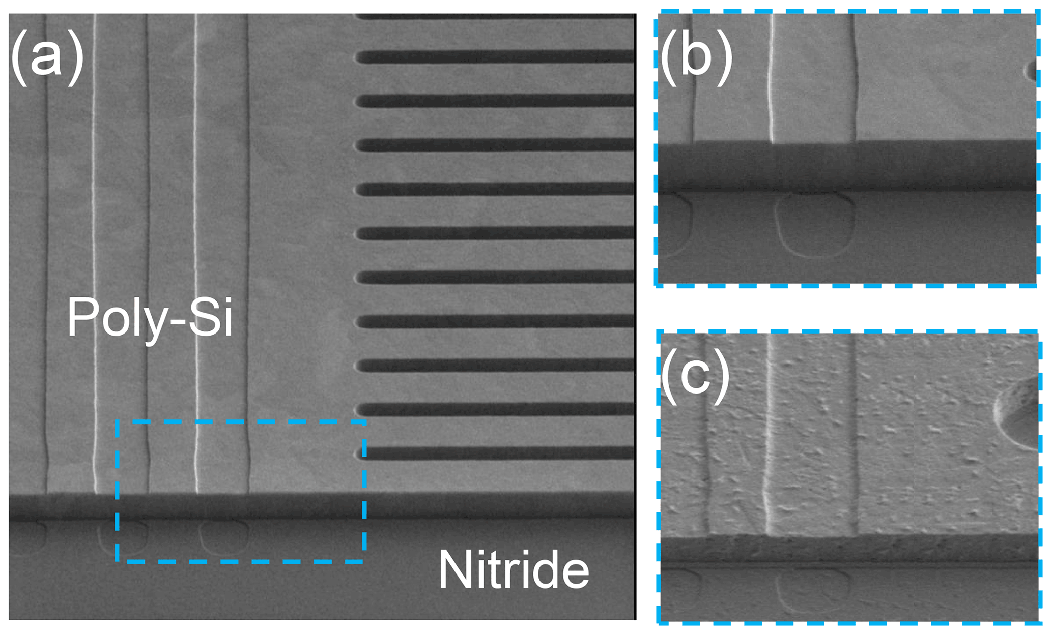
Figure 5Influence of subsequent dry-etching processes on the surface roughness of the polysilicon (Poly-Si). (a) SEM image taken after waveguide and grating etch. Panels (b) and (c) represent a magnified view of the marked area (blue dashed rectangle) before and after treatment with a silicon dry-etching sequence following the wet-chemical metal etch of AlSiCu, respectively. All SEM images are taken with a tilt of 30∘.
In order to avoid this kind of damage, one can substitute the material used for metallization. In the described context, pure Al or AlCu constitute suitable alternatives, as these materials allow wet-chemical etching without the need of a subsequent dry-etching process that might be harmful for the underlying polysilicon.
The structuring of the AlN is more challenging, as substituting the layer is not an option. The pyroelectric properties form the envisioned IR detector correspond to the use of this material. The structuring of this layer is done by means of lithography and a dry-etching process, which employs chlorine chemistry as an etchant. As revealed by Fig. 6a and b, the chlorine has no or too little selectivity between AlN and polysilicon. Thus, a short sequence of over-etching causes significant damage to the polysilicon structures. In this case, the damage is so strong that in-coupling of laser light and transmission through the waveguide is no longer possible, which corresponds to a damping value of D>10 cm−1. However, over-etching is necessary to ensure a uniform processing across the 8 in. (= 200 mm) wafer without leaving AlN residuals. Therefore, a protection concept is required. The schematic in Fig. 7a–d describes one approach to prevent the polysilicon structures from damage corresponding to the structuring of the AlN layer.
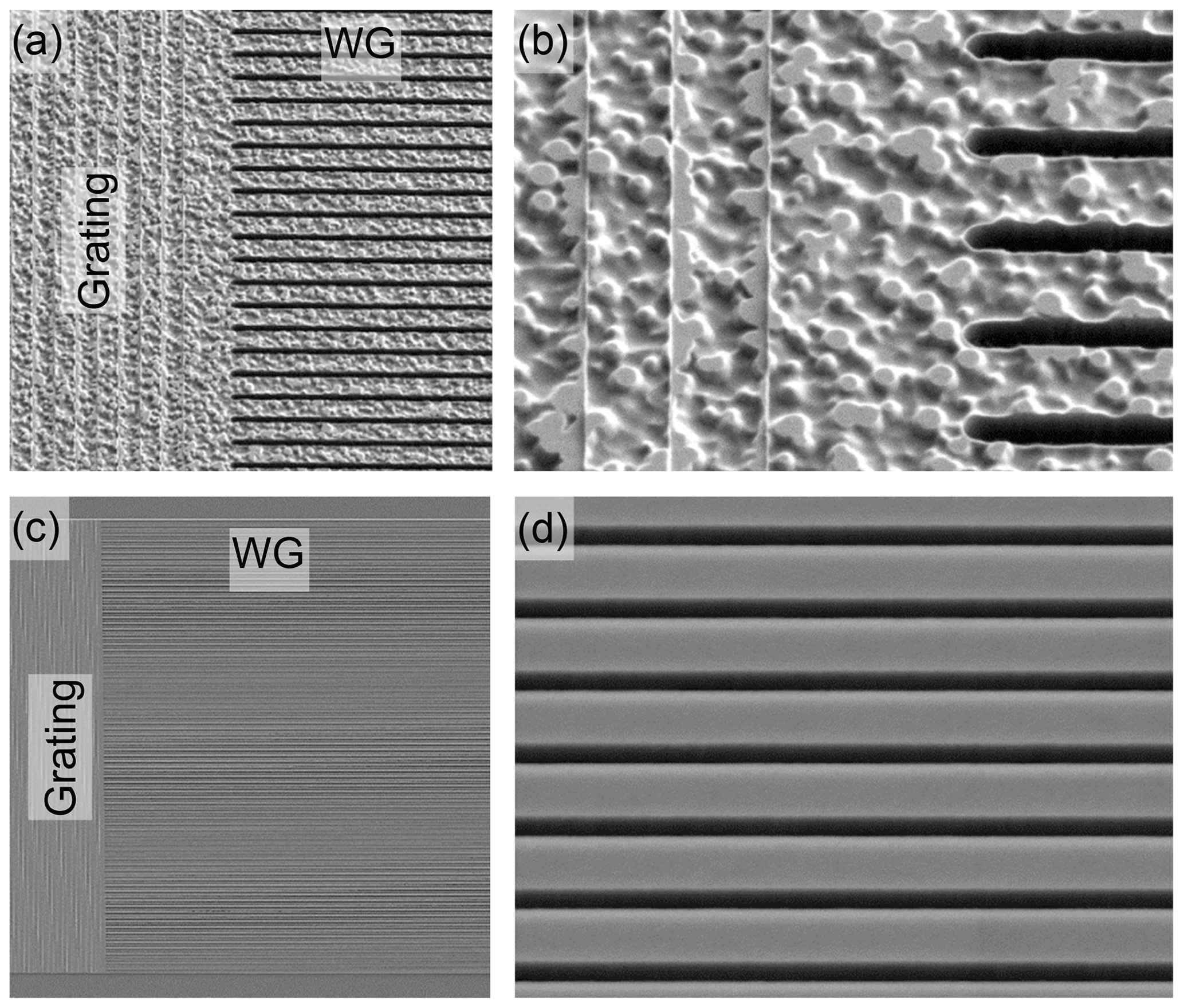
Figure 6SEM images of unprotected and protected waveguide structures after the AlN dry-etching process. (a) The unprotected polysilicon appears very rough. The coupler grating and the waveguide area is visibly harmed. (b) Magnified view of a coupler grating to waveguide transition. (c) Protected structures, after removal of the residuals of the sacrificial oxide layer, taken form the wafer center. These samples do not show much damage, as revealed by the magnified view in panel (d). All SEM images are taken with a tilt of 30∘.
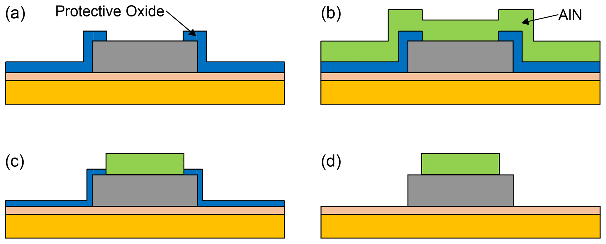
Figure 7Schematic process flow to protect the polysilicon waveguides during subsequent dry-etching processes. (a) Deposition and structuring of a silicon oxide that should act as an protective layer. (b) Sputtering of AlN. (c) Structuring of the AlN layer by means of lithography and dry etching. During the over-etching sequence of the AlN etch, the protective oxide becomes thinner (sacrificed) but is not completely consumed. (d) Wet-chemical cleaning to remove the residuals of the sacrificial oxide. The AlN remains only at the structures that form the detector.
The idea is to deposit a silicon oxide layer (∼400 nm) on top of the polysilicon and underneath the AlN, at the area where the AlN has to be removed (see Fig. 7a and b). It should act as a sacrificial etch stop layer and is chosen to be thick enough to accommodate an appropriate over-etching sequence without being entirely consumed (see Fig. 7c). A subsequent cleaning step removes the residual silicon oxide and reveals the underlying structures (see Fig. 7d).
The SEM images in Fig. 6c and d reveal the achieved quality of the waveguide structures fabricated that employ the introduced process flow to protect the polysilicon. While structures at the wafer edge still suffer from damage caused by the etching process, the structures at the wafer center show almost no such damage. The different quality of structures taken from the wafer center or edge is most likely linked to an insufficient uniformity of the dry-etching sequence with a varying etch rate across the wafer. In this context, increasing the thickness of the protective oxide layer or adapting process parameters of the dry-etching sequence are possible ways to further increase the yield of undamaged structures.
Figure 8 reveals the experimental results retrieved for protected waveguide structures taken from the wafer center. The measured intrinsic damping of the corresponding structures is of the order of cm−1. The experimental value for structures taken from the wafer edge is found to be cm−1. Therefore, we can state that the described sequence is capable of protecting the waveguide structures from damage linked to the dry-etching process to structure the AlN layer. In particular, the waveguides taken from chips located at the wafer center reveal the potential of the described protecting sequence. The feasibility of integrating an AlN-based pyroelectric detector for the mid-IR together with sensitive, low loss, polysilicon waveguide structures constitutes a huge leap, with respect to the fabrication, towards a monolithic, fully integrated NDIR sensor system for on-chip gas measurements. In particular, this feasibility could pave the way for a generation of gas sensors combining high sensitivity and a small footprint.

Figure 8Determination of waveguide damping for protected waveguide structures taken from the wafer center. The linear fit reveals a damping of the order of cm−1 (red dashed line).
Motivated by the idea to build an interesting platform for absorption spectroscopy using the evanescent field of the guided light, we have successfully demonstrated the fabrication and characterization of integrated plasmonic waveguide structures for mid-IR radiation. The target geometry of the fabricated multi-strip structures, retrieved from simulations, was chosen to be a 1.3 µm strip width, separated by 0.4 µm wide air gaps. The experimental values of the confinement factor and intrinsic damping could be determined to Γexp=14.6 % and Dexp=1.6 cm−1, respectively, which meets the expectations from simulations when imperfections from fabrication are considered. Furthermore, as the suggested structures could also be integrated in a sensor system comprising a thermal emitter, a spectral filter, and an IR detector, we investigated a process sequence, to maintain the low intrinsic damping throughout a range of processes needed for emitter and detector integration. In particular, the described sequence is capable of protecting the polysilicon waveguide structures from damage linked to a dry-etching processes, employing chlorine chemistry as an etchant. Even though the uniformity of the processing can still be further improved, this work demonstrates the feasibility of integrating an AlN-based, pyroelectric detector for the mid-IR together with sensitive, low loss, polysilicon waveguide structures.
Software code underlying the results presented in this paper are not publicly available at this time but may be obtained from the authors upon reasonable request.
Data underlying the results presented in this paper are not publicly available at this time but may be obtained from the authors upon reasonable request.
GS, CC, PT, AT, KFO, and BU did the characterization and analysis. CF, AT, TG, EA, and BJ acquired the funding and administered the project. GS and KC were responsible for the design and fabrication. CC, GP, and PS did the simulations. CC, CF, AT, RJ, TG, and BJ acted as supervisors. GS, KC, and TG developed the concept to protect the waveguides. GS prepared the paper, with contributions from all co-authors.
The contact author has declared that none of the authors has any competing interests.
Publisher's note: Copernicus Publications remains neutral with regard to jurisdictional claims in published maps and institutional affiliations.
This article is part of the special issue “MikroSystemTechnik Kongress 2021”. It is a result of the “MikroSystemTechnik Kongress 2021”, Ludwigsburg, Germany, 8–10 November 2021.
The authors want to thank the process experts at Infineon Technologies Austria AG, for their support in the fabrication and the fruitful discussion during process development and integration phase.
This project was performed within the COMET Centre ASSIC Austrian Smart Systems Integration Research Center, which is funded by BMK, BMDW, and the Austrian provinces of Carinthia and Styria, within the framework of COMET – Competence Centers for Excellent Technologies. The COMET programme is run by FFG (grant no. 865890).
This paper was edited by Michael Kraft and reviewed by two anonymous referees.
Consani, C., Ranacher, C., Tortschanoff, A., Grille, T., Irsigler, P., and Jakoby, B.: Mid-infrared photonic gas sensing using a silicon waveguide and an integrated emitter, Sensor. Actuat. B, 274, 60–65, https://doi.org/10.1016/j.snb.2018.07.096, 2018. a, b
Cordes, K.-H., Waag, A., and Heuck, N.: Integrierte Schaltungen Grundlagen – Prozesse – Design, Pearson Deutschland, https://elibrary.pearson.de/book/99.150005/9783863266769 (last access: 10 June 2022), 2010. a
Costa, R., Melloni, A., and Martinelli, M.: Bandpass resonant filters in photonic-crystal waveguides, IEEE Photon. Technol. Lett., 15, 401–403, https://doi.org/10.1109/LPT.2002.807953, 2003. a
Eberl, M., Jost, F., Kolb, S., Schaller, R., Dettmann, W., Gassner, S., and Skorupa, F.: Miniaturized photoacoustic CO2 gas sensors – A new approach for the automotive sector, in: AmE 2019 – Automotive meets Electronics, 10th GMM-Symposium, 12–13 March 2019, Dortmund, Germany, 1–5, ISBN 978-3-8007-4877-8, https://ieeexplore.ieee.org/stamp/stamp.jsp?tp=&arnumber=8727851&isnumber=8727837 (last access: 8 August 2022), 2019. a
Jannesari, R., Ranacher, C., Consani, C., Grille, T., and Jakoby, B.: Sensitivity Optimization of a Photonic Crystal Ring Resonator for Gas Sensing Applications, Sensor. Actuat. A, 264, 347–351, https://doi.org/10.1016/j.sna.2017.08.017, 2017. a
Kischkat, J., Peters, S., Gruska, B., Semtsiv, M., Chashnikova, M., Klinkmüller, M., Fedosenko, O., Machulik, S., Aleksandrova, A., Monastyrskyi, G., Flores, Y., and Masselink, W. T.: Mid-infrared optical properties of thin films of aluminum oxide, titanium dioxide, silicon dioxide, aluminum nitride, and silicon nitride, Appl. Optics, 51, 6789–6798, https://doi.org/10.1364/AO.51.006789, 2012. a
Lavchiev, V. M. and Jakoby, B.: Photonics in the Mid-Infrared: Challenges in Single-Chip Integration and Absorption Sensing, IEEE J. Select. Top. Quant. Elect., 23, 452–463, https://doi.org/10.1109/JSTQE.2016.2619330, 2017. a
Němec, H., Kužel, P., Duvillaret, L., Pashkin, A., Dressel, M., and Sebastian, M. T.: Highly tunable photonic crystal filter for the terahertz range, Opt. Lett., 30, 549–551, https://doi.org/10.1364/OL.30.000549, 2005. a
Ng, D. K. T., Ho, C. P., Xu, L., Chen, W., Fu, Y. H., Zhang, T., Siow, L. Y., Jaafar, N., Ng, E. J., Gao, Y., Cai, H., Zhang, Q., and Lee, L. Y. T.: NDIR CO2 gas sensing using CMOS compatible MEMS ScAlN-based pyroelectric detector, Sensor. Actuat. B, 346, 130437, https://doi.org/10.1016/j.snb.2021.130437, 2021. a
Pühringer, G., Consani, C., Jannesari, R., Fleury, C., Dubois, F., Spettel, J., Dao, T. D., Stocker, G., Grille, T., and Jakoby, B.: Design of a Slab Tamm Plasmon Resonator Coupled to a Multistrip Array Waveguide for the Mid Infrared, Sensors, 22, 2968, https://doi.org/10.3390/s22082968, 2022. a
Ranacher, C., Consani, C., Jannesari, R., Grille, T., and Jakoby, B.: Numerical Investigations of Infrared Slot Waveguides for Gas Sensing, Proceedings, 2, 799, https://doi.org/10.3390/proceedings2130799, 2018a. a
Ranacher, C., Consani, C., Tortschanoff, A., Jannesari, R., Bergmeister, M., Grille, T., and Jakoby, B.: Mid-infrared absorption gas sensing using a silicon strip waveguide, Sensor. Actuat. A, 277, 117–123, https://doi.org/10.1016/j.sna.2018.05.013, 2018b. a
Ranacher, C., Consani, C., Vollert, N., Tortschanoff, A., Bergmeister, M., Grille, T., and Jakoby, B.: Characterization of Evanescent Field Gas Sensor Structures Based on Silicon Photonics, IEEE Photon. J., 10, 1–14, https://doi.org/10.1109/JPHOT.2018.2866628, 2018c. a
Ranacher, C., Consani, C., Tortschanoff, A., Rauter, L., Holzmann, D., Fleury, C., Stocker, G., Fant, A., Schaunig, H., Irsigler, P., Grille, T., and Jakoby, B.: A CMOS Compatible Pyroelectric Mid-Infrared Detector Based on Aluminium Nitride, Sensors, 19, 2513, https://doi.org/10.3390/s19112513, 2019. a, b, c
Stocker, G., Consani, C., Thakkar, P., Tortschanoff, A., Fleury, C., Puehringer, G., Jannesari, R., Saeidi, P., Grille, T., Kovatsch, C., Bartl, U., Aschauer, E., and Jakoby, B.: Fabrication of integrated poly-silicon wave guides for mid-infrared absorption spectroscopy using the evanescent field, in: MikroSystemTechnik Congress 2021, 8–10 November 2021, Stuttgart-Ludwigsburg, Germany, 148–151, ISBN 978-3-8007-5656-8, 2021. a
- Abstract
- Introduction
- Fabrication of multi-strip waveguide structures
- Characterization of multi-strip waveguide structures
- Maintaining waveguide quality throughout the fabrication
- Summary
- Code availability
- Data availability
- Author contributions
- Competing interests
- Disclaimer
- Special issue statement
- Acknowledgements
- Financial support
- Review statement
- References