the Creative Commons Attribution 4.0 License.
the Creative Commons Attribution 4.0 License.
 | 23 Mar 2022
Assembly and interconnection technology for high-temperature bulk acoustic wave resonators
Fabian Kohler
Monika Farina
Michal Schulz
Holger Fritze
Jürgen Wilde
A sensor based on a piezoelectric single crystal enables operation even under harsh environmental conditions. In addition to the sensor element, the packaging technology is crucial for sensor performance. In this paper, a suitable assembly and interconnection technology concept of Ca3TaGa3Si2O14 (CTGS) resonators for high-temperature applications is presented as a platform for future sensor assemblies. The concept described here has already been functionally tested as a temperature sensor (Schulz et al., 2021).
The concept includes a sapphire base plate, a housing lid, and a spacer made from aluminium oxide (Al2O3). The substrate is metallised with platinum manufactured into thin film and thick film technology. The ceramic components are fused with glass solder. The connection of the resonator to the conductive tracks is realised by thermosonic bonding with 25 µm platinum wire. Initially, the stability of the metallisation must be investigated before subsequent electrical testing under high temperature. Diffusion processes play a major role in this temperature range, and the stability of the layer is a necessary condition for subsequent investigations. A suitable set of bonding parameters and the strength of the platinum bonds prior to and after thermal load is analysed.
Shear tests are used to evaluate the quality of the ceramic materials fused with glass solder after thermal ageing. The dielectrical properties of sapphire and glass solder such as the isolation resistance, the relative permittivity, and the loss factor at high temperatures are evaluated using interdigital structures. The loss factor is measured on both bare interdigital structures and the samples coated with glass solder to make an estimation about the conductive behaviour up to 1000 ∘C. A ceramic lid for the sensor housing is attached by a high-temperature stable glass solder. Since platinum conductors are fed through this glass solder connection, the electrical conductivity of the glass solder is characterised at high temperature. Furthermore, the hermeticity of the assemblies is verified by means of helium leakage tests.
These investigations are the basis for the implementation of an assembly and interconnection technology that is suitable for reliable operation under extreme temperature conditions. The packaging technology also offers further possibilities for pressure or chemical sensors that can withstand high-temperature loads.
- Article
(5766 KB) - Full-text XML
- Companion paper
- BibTeX
- EndNote


A reliable system for high-temperature applications requires not only a sensing device but also a robust design and assembly technology that protects the sensor in harsh environmental conditions. Components based on piezoelectric single crystals have the potential to be used as sensors at extreme temperatures (Fritze et al., 2003). In order to give these sensors a platform that also functions under high-temperature conditions (1000 ∘C), the following objectives were defined:
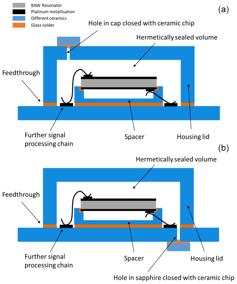
Figure 1Schematic diagram of the sensor set-up as a temperature sensor. (a) A hole in a ceramic cap sealed with a Al2O3 chip and glass solder. (b) A hole in sapphire sealed with a Al2O3 chip and glass solder.
-
material selection with suitable thermomechanical properties
-
reliable interconnection technology with a suitable metallisation system
-
sufficient electrical insulation properties of the substrate material.
With regard to the packaging and interconnection technology, physical properties such as electrical and mechanical damping, as well as electrical conductivity, have to be considered with regard to the sensor functionality.
Another challenge is the reliability at temperatures up to 1000 ∘C. Platinum wire bonding was used as the interconnection technique. Glass solders show good bonding and sealing properties for housing elements at high temperature (Zang et al., 2012). The adaptation of these materials to the expansion coefficients of the joining partners enables low-stress bonds. The composite properties of glass–ceramic solders result from the properties of the glassy and the crystalline phases, according to the rules of mixtures. Sensor designs that have already been implemented are often limited in terms of maximum temperature (Subbiah et al., 2018; Zeiser, 2015).
The sensor concept presented here can be used as a base for various sensor set-ups. Figure 1 shows the set-up as a temperature sensor. The package includes the electrical connections using platinum metallisation and wire bonds, a metallised ceramic carrier, and glass solders to connect the individual components.
Table 1Challenges and possible solutions to the presented high-temperature assembly technology.
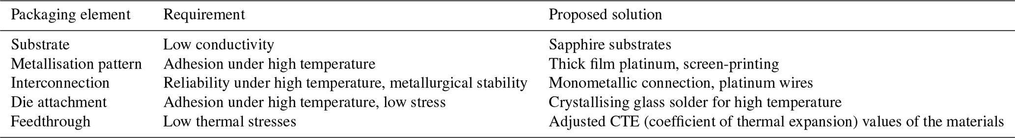
The challenges summarised in Table 1 result from an analysis of the schematic diagram. Possible solutions in Table 1 were derived based on previous experience and on theoretical assessment. They will be validated further in this paper.
The dielectric properties of the sapphire substrates up to 1000 ∘C are determined by conductivity measurements. The temperature resistance of the metallisation and interconnection technology is analysed by optical analysis and wire pull-off tests before and after thermal ageing at 1000 ∘C. The quality of the glass solder joint is tested by shear tests after thermal stress. The hermeticity of the sensor housing is verified by helium leakage tests after assembly and after thermal stress, up to 112 h, at 1000 ∘C.
This results in the systematic development of an assembly and interconnection technology for high-temperature applications that are based on metallurgical, thermomechanical, and electrical compatibility.
At working temperatures of 1000 ∘C, the use of conventional piezoelectric ceramics like lead zirconate titanate (PZT) is impossible because their Curie temperature TC, at which the ferroelectric order disappears, is too low. Due to its reported maximum operating temperature of 1370 ∘C (Fu et al., 2016), Ca3TaGa3Si2O14 (CTGS) was chosen as resonator material in this work. Furthermore, CTGS exhibits an ordered crystal structure and shows improved electromechanical properties, particularly lower acoustic losses than disordered crystals (Suhak et al., 2018; Yu et al., 2011).
Table 2Materials for system integration with estimated maximum operating temperature (Damjanovic, 1998; Zang et al., 2012).
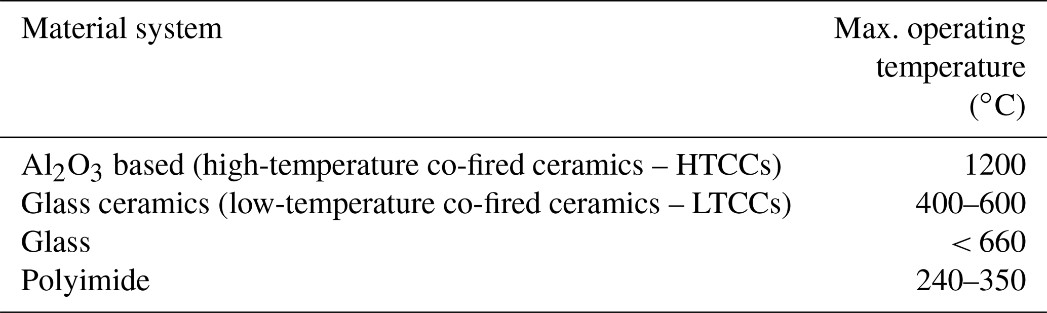
2.1 High-temperature ceramics
With their temperature stability, ceramics are the sole potential materials for high-temperature packaging. Table 2 shows typical materials for system integration with their maximum operating temperature.
The maximum operating temperatures in Table 2 allow that high-temperature co-fired ceramics (HTCCs) can be used as substrate material up to 1200 ∘C. Other parameters to be considered are electrical conductivity and CTE. Alumina is used as a standard substrate material in sensors and powered electronics. It is particularly suitable because of its high-temperature stability and its chemical resistance. Alumina is one of the most commonly used advanced ceramic materials. As a low-cost material, it is used in many commercial applications. In addition, the availability in highly purified grades makes it very popular in advanced materials research studies. Ceramic materials based on oxide, nitride, and carbide show thermal shock resistance owing to their high thermal conductivity, low CTE, and high strength (Lv et al., 2021). Therefore, they are suitable for high-temperature applications. Depending on the purity, alumina can be used up to 1700 ∘C and is able to seal gases up to 1300 ∘C (Hassanin, 2011; Oezkan and Moulson, 1970).
Sapphire is a single crystalline modification of Al2O3 with a trigonal crystal system. It exhibits high purity, and it has no glass content and no grain boundaries. This means that unwanted deformation mechanisms and electrical conductivity due to doping and grain boundary effects can be avoided. In this work, substrates of sapphire in a C-plane orientation are used.
2.2 Platinum metallisation
Possible deposition processes for platinum on ceramic materials are the thin and thick film technology. Both types of metallisation were used to generate the conductors on the sensor structure and the package. For both, good adhesion must be assured even after thermal ageing. Also, the bondability with thin platinum wires is a prerequisite for further signal routing. In order to ensure a monometallic connection with thin platinum wires, platinum metallisations are examined in more detail in the following sections. A scanning electron microscope (SEM) is used for visual examination of the surface.
2.2.1 Thin film metallisation
The thin film metallisation is realised for coplanar interdigital electrodes (IDE), which are ideal for dielectric measurements. The interdigital electrodes are structured by photolithography and lift-off technique.
The platinum is deposited in a sputtering process as a two-layer system. For better adhesion to the sapphire, an adhesion promoter layer of 20 nm titanium is deposited prior to sputtering the 200 nm thick Pt layer. Sputtering is performed with 400 W DC power and a deposition rate of 0.2 nm s−1. To avoid overheating of the substrate, sputtering is performed in four steps for 250 s each.
The sputter target is made of platinum with a purity of 99.95 %, a diameter of 90 mm, and a thickness of 6 mm.
To obtain information on how the sputtered thin film on sapphire behaves under high temperature, thermal ageing tests are performed.
2.2.2 Thick film metallisation
The thick film pattern is carried out using the platinum paste, C3620, purchased from Heraeus. According to the data sheet, this paste forms a purely metallic surface on AlN and Al2O3 after the firing process. For Al2O3, a purity of 96 % is specified. The platinum thick film pattern is produced by a screen-printing process. Firing at 850 to 1400 ∘C peak temperature for 9 to 11 min is recommended in the data sheet. Firing temperatures up to 1100 ∘C were tested in preliminary experiments. For the preparation of the thick film samples considered here, a firing temperature of 1000 ∘C and 10 min holding time is used. The resulting layer thickness after the firing process is approximately 15 µm.
2.3 Glass frit bonding
A commonly used joining technique for high-temperature applications is the glass frit bonding. This technique offers high bond strength and process yield, controllable stresses at the bond interface, and accurate process reproducibility. There are two types of glass frits named vitreous and devitrifying. Vitreous glass frit is thermoplastic in nature and melts and flows every time it is reheated to the sealing temperature. Devitrifying glass frit, on the other hand, is a thermosetting material that crystallises during the sealing temperature steps. Its softening temperature increases during crystallisation (Zang et al., 2012). Glass frit bonding requires the use of a meltable glass powder, organic binder, inorganic fillers, and solvents. The organic binder transforms the glass powder into a printable viscous paste (Knechtel et al., 2006).
The glass powder is generally made up of network formers, modifiers, and intermediates (Tyagi et al.,2017). Network formers (e.g. SiO2, B2O3, GeO2, and P2O5) are oxide forming glasses that can form 3D covalent networks via bridging oxygen. Network modifiers (e.g. Li2O, K2O, Na2O, MgO, CaO, and PbO) are ionic oxides added to lower the processing temperature by weakening the bonds. This also decreases the glass transition temperature (Tg). Intermediates (e.g. Al2O3, TiO2, and ZrO2) are additives that are added in small quantities to improve the thermal and mechanical behaviour of the glass by adding interatomic space to the structure, which allows room for movement. The CTE is defined by the contents of the glass matrix and the filler via a rule of mixtures. Inorganic fillers are used to match the CTE of the glass frit material to the substrate material (Zeitouny, 2021).
Table 3Composition of the glass solder, G018-385, according to manufacturer's specifications.
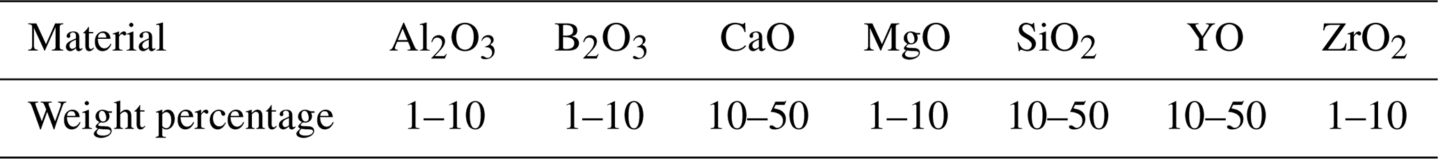
In this research, the glass frit of Schott G018-385 was used. The main constituents are the network modifiers and network formers of yttrium oxide, silicon oxide, and calcium oxide with nearly equal weight percentages. This is a crystallising joining glass for high-temperature applications. As a devitrified glass frit, it is initially glassy and crystallises into a solid bond.
The glass solder is applied as a paste via a stencil printer. The ring stencil with a thickness of 100 µm has two narrow bars through which no material is applied. These gaps are closed by the pasty material behaviour and the associated cohesive forces. Reference marks allow exact alignment with the sapphire substrate. The paste is pre-dried in a convection oven and then fired at a temperature of 950 ∘C for 30 min.
In order to take a closer look at the influence of surface roughness on the joint quality of the glass solder joints, the sapphire surfaces were structured using a marking laser by TRUMPF (TruMark 6350). Both a line pattern and a circular pattern were scanned with this laser. The surface roughness was measured using a white light interferometer. The 650 µm thick substrates were cut from a wafer which is polished on one side. Therefore, both the unpolished and the polished side were considered in the analysis.
To investigate the adhesion strength, shear tests were carried out on 2 mm by 2 mm alumina chips, which were glass-soldered onto different surfaces. The sample size was nine chips per surface.
2.4 Shear test
The shear tests are used to evaluate the mechanical strength of the glass frit fusion bond between the Al2O3 and the sapphire substrate. Parts of 2 mm by 2 mm of Al2O3 are used for the shear tests. The shear strength is usually expressed as the maximum shear force per area of the glass frit. A DAGE series 4000 shear force measurement tool is used to apply an increasing shear force to a die until fracture occurs. The direction of the applied force is perpendicular to the die edge and parallel to the substrate plane. The tests were performed at room temperature with a shear height of 300 µm at a tool speed of 300 µm s−1.
2.5 Platinum interconnection
For the electrical interconnection of the resonator to the platinum conductors on the substrate, platinum wire bonding was evaluated. Metallisation and interconnections form a monometallic system. In that way, an attempt was made to avoid degrading metallurgical reactions and to prevent stress problems due to matched thermal expansion coefficients.
The most important process parameters for the formation of a micro-welded joint are bonding force FB, ultrasonic power PUS, and ultrasonic duration tUS for thermosonic wire bonding and the temperature of the specimen holder. The bonding force is applied to the bonding wire to create a mechanical bond to the substrate surface. The application of ultrasonic energy and the associated oscillating motion of the bonding tool causes softening of the bonding wire, local heating, and cleaning of the metallic substrate surface. The interaction of temperature, ultrasound, and force thus creates small solid-state bonds between the joining partners.
In addition to the bond parameters, the cause of failures is also examined in more detail. The following failure mechanisms are observed: delamination of the bond pad from the substrate, detachment of the bond foot from the bond pad (lift-off), wire failure at the heel due to pre-damage of the wire in the welding process, and wire fracture in the loop.
The failure mechanism of bonding wires before and after thermal ageing can be used to provide additional information about the adhesion strength of the metallisation to the substrate.
For the evaluation of thermal influences on the adhesion strength of the metallisations on the substrates and the wire bonds, 25 wires, each with a diameter of 25 µm, are bonded to thin films and thick films, using a Delvotec 5430 wedge bonder, with the following parameters:
-
0.47 N bond force
-
400 mW ultrasonic power
-
60 kHz ultrasonic frequency
-
50 ms bonding time
-
300 ∘C substrate temperature.
The subsequent pull test determines the maximum force of the connection, and the failure mechanism is recorded.
Table 4Coefficient of the thermal expansion of the materials used according to the literature and the manufacturer's specifications.
2.6 Thermo-mechanical stresses
The CTE of the packaging material is one of the principal parameters in reducing the thermally induced stresses. The materials used for sensor chip, substrate, and die attachment should closely match in CTE to avoid different expansion and stress to the sensor. Residual stresses may influence the properties of the housed transducer structures and also the long-term reliability of the bond frame. Therefore, the determination of the residual stress level provides information for optimisation of device performance and reliability.
The long-term mechanical stability of the package is an important aspect for the reliability in the assembly and interconnection technology of sensor systems. Since the glass frit bond frame is subjected to thermal stresses due to different thermal expansion coefficients of glass, sapphire, and aluminium oxide, it constitutes a potential weak link in the package. Therefore, a stable bonding approach on a glass frit bonded device has to carefully consider all the possible failure mechanisms.
The wide range of the reported CTE value of sapphire in Table 4 can be explained by the temperature range from 20 up to 1000 ∘C. The values of platinum, glass solder, and aluminium oxide are for the temperature range from 20 to 300 ∘C. In addition to the temperature dependence, a possible non-linear behaviour of the CTE values in the temperature range up to 1000 ∘C must be taken into account. Table 4 shows the good match of the CTE value of the glass solder with the alumina material of the housing lid of 8.5 ppm K−1. Furthermore, the platinum lies in the range of 9 ppm K−1. The single crystalline sapphire shows the lowest value with 6.6 ppm K−1.
2.7 Electrical conductivity
The capacitive measurements at temperatures up to 1000 ∘C can be used to determine the electrical behaviour of the sapphire and the glass solder material. It was assumed that the electrical conductivity of the sapphire is relatively low due to the high purity. For the glass solder material, a higher number of mobile charges must be expected for this multi-ionic and partly amorphous material.
The measurements were performed in a frequency range from 500 kHz to 2 MHz, using a Keysight E4980A Precision LCR (inductance (L), capacitance (C), and resistance (R)) meter. The test specimens are formed by 200 nm thin interdigital structures which are sputter-deposited onto the sapphire substrates. In the test samples, the total number of fingers is 124, whereas the width of the interdigital structures and the distance between the fingers are 40 µm each. The length of the fingers is 10 mm.
The relative permittivity εr of the sapphire with interdigital electrodes is calculated according to the following formula (Alley, 1970):
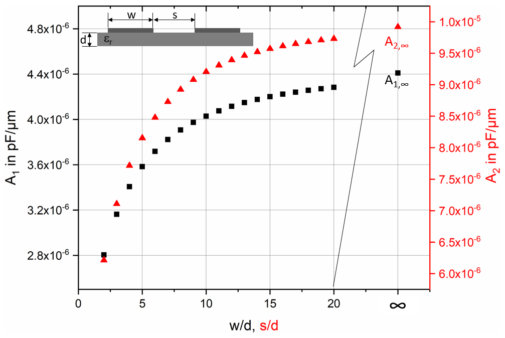
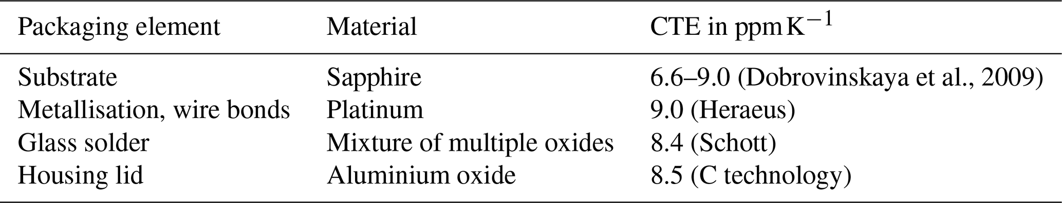
Figure 2Progression of the geometry factors A1 and A2 for Eq. (1), adapted according to Alley and Bahl (Alley, 1970; Bahl, 2003).
Here the dimension l denotes the length of the fingers, Cp the capacitance, and N the number of fingers. Figure 2 shows the progression of the geometry factors A1 and A2 over the relationship of and , respectively, where d is the thickness of the substrate (see Fig. 2).
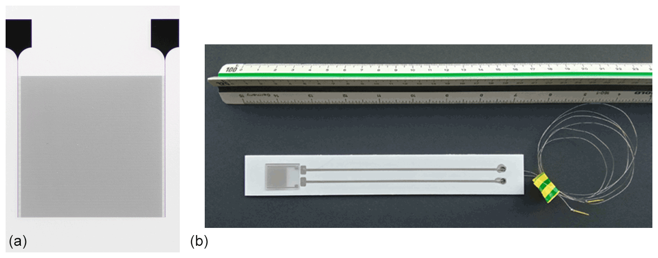
Figure 3(a) The 200 nm thin film platinum comb structure on sapphire substrate. (b) Measurement set-up with conductive tracks for installation in the furnace (Farina, 2021).
For a measurement without a ground plane, the geometry factors A1 = 4.409 × 10⁻⁶ pF µm−1 and A2 = 9.92 × 10⁻⁶ pF µm−1 can be used when the conductor width w and the spacing s are both much larger than the substrate thickness.
For the measurement of permittivity over temperature, the temperature is increased in steps of 100 K, starting from room temperature. The measurement was carried out under vacuum (pressure range of 10−4 mbar).
The measurement structure was contacted with the help of platinum conducting tracks (Fig. 3).
The electrical equivalent circuit of the set-up includes a parallel capacitance and an associated parallel resistance. The cable resistances of the wires are combined in a serial resistor Rs. The cables also represent a parallel capacitance Cs to the measured capacitance (Fig. 4).
Figure 4Electrical equivalent circuit of the measurement set-up for capacitance measurement.
After coating the interdigital structure with glass solder, the temperature-dependent impedance of the glass solder can be examined. For multilayer substrate interdigital capacitors, this extends to the partial capacitances of the individual layers as follows (Gevorgian, 1996):
Here Cn0 represents the air filling, Cn1 is the substrate (sapphire), Cn2 is the superstrate (platinum), and the Cn3 is the cover layer (glass solder).
2.8 Hermeticity analysis
The connection between the sapphire and the aluminium oxide cap is a potential leakage point. The housing caps were applied under normal atmospheric pressure. To avoid the de-wetting of the annular glass solder joint, the sealing process was divided into two separate glass soldering steps.
Uniform outgassing of the organic binders can be realised through a hole in the cap and via a hole in the sapphire substrate (Fig. 1).
The subsequent closure takes place by a ceramic chip visible in Fig. 1, using a further glass soldering process step. The smaller and selectively concentrated solder volume prevents the formation of leak paths to the outside, which could be observed when soldering without a hole in cap or sapphire.
To analyse the leakage rate, the assembly is stored in a helium chamber for at least 5 h in accordance with the standard MIL-STD-883G (Department of Defense Test Method Standard, 2022). During the subsequent test, the helium leaking to the outside is measured using a mass spectrometer. According to the standard, a leak rate of 5 × 10⁻⁸ mbar L s−1 should not be exceeded for the enclosure, since the inner volume of the package is 1.57 cm3 .
3.1 Comparison of metallisation systems
The conductors on the sensor structure and the package are realised both in thin film and thick film technology. For both variations, good adhesion must be ensured even after thermal ageing. Whereas, for thin platinum layers, it is known that degradation already takes place in the temperature range of 700 ∘C (Bernhardt et al., 2001), it can be assumed that the thick film paste is more temperature stable due to its high-temperature firing process. Also, the bondability with thin platinum wires and their stability at elevated temperatures is a prerequisite for further signal routing. In order to ensure a monometallic interconnection with thin platinum wires, both metallisation systems are examined in more detail in the following sections. A scanning electron microscope (SEM) is used for visual examination of the surface.
3.1.1 Thin film metallisation investigation
In the first step, the interdigitated structures are aged for 6 h at 800 ∘C. This shows that the previously straight edge indicates fraying in the edge area very quickly (Fig. 5 right).
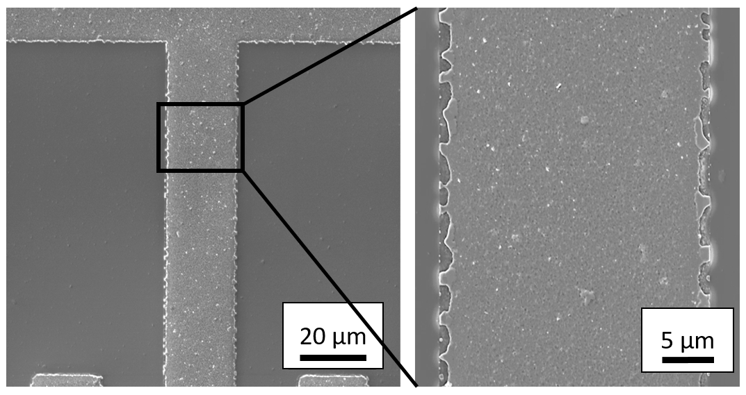
Figure 5SEM image of a thin film layer (20 nm Ti; 200 nm Pt) after thermal ageing for 6 h at 800 ∘C.
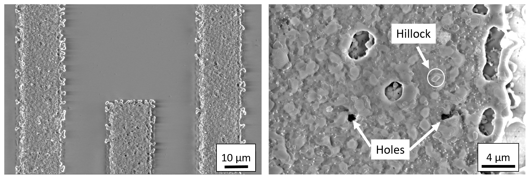
Figure 6SEM image of a thin film layer (20 nm Ti; 200 nm Pt) after thermal ageing for 6 h at 1000 ∘C.
When a similarly fabricated thin film structure is aged for 6 h at 1000 ∘C, the de-wetting processes can be observed clearly (Fig. 6). Furthermore, material accumulations can be seen as hillocks. Holes begin to form on the metallic surface. Based on these results, we assumed that the platinum thin films are not stable enough for extended use at the addressed high temperature. Also, the diffusion of the titanium into the platinum layer could worsen the adhesion of the platinum to the sapphire.
Based on the phase diagram and due to the low percentage of the 20 nm titanium under the 200 nm platinum layers, complete dissolution of the titanium in the platinum must be expected at elevated temperatures. Consequently the effect of titanium as an adhesion promoter is no longer given and de-wetting can occur. A possibility for maintaining adhesion is the use of tungsten, tantalum, or zirconium as intermediate layers (Seifert et al., 2017).
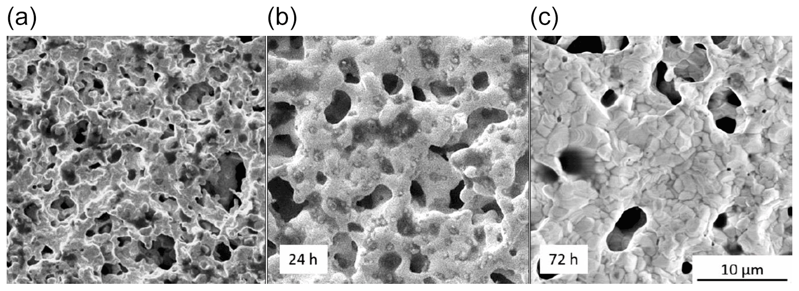
Figure 7SEM image of a screen-printed substrate with a platinum thick film paste (a) before, (b) after 24 h, and (c) after 72 h of thermal ageing at 1000 ∘C.
3.1.2 Thick film metallisation investigation
In preliminary investigations, the thick film metallisation had shown no ageing effects after 6 h at 800 ∘C. The thermal ageing of a screen-printed thick film paste for 24 h at 1000 ∘C shows that the surface of the layer changes further during a longer holding times up to 72 h (Fig. 7). The initially highly porous surface reveals larger grains (Fig. 7 mid), but the surface shows fewer and larger pores. After thermal ageing for 72 h, further grain growth and coalescence of the porous areas is evident.
It can be concluded from this investigation that the 10 min firing step has not completed the sintering process step of the platinum paste. In order to obtain more stable sinter layers on which wire bonds can be reliably placed, a subsequent firing step at 1000 ∘C is added to the thick film metallisation process. This subsequent firing process completed the sintering process of the platinum paste.
A consideration of thick film and thin film metallisation after thermal ageing in this work shows the potential suitability of thick film metallisation systems up to temperatures of 1000 ∘C. As no improvement in the density of the sintered structure could be observed in a comparison of 1000 and 1100 ∘C, the use of an alternative paste system is planned for further investigations. According to the manufacturer, this material should sinter more densely.
3.2 Platinum wire bonding
Wire bond pull tests are used to characterise the adhesion of the bonds to the metallic surfaces. Tests are carried out before and after thermal ageing for 6 h at 800 or at 1000 ∘C. Figure 8 shows the metallisation delamination as being the cause of failure after thermal ageing at 800 ∘C for 6 h of a platinum bond wire on thin film metallisation.

Figure 8Wire bond on Pt thin film before (a) and after (b) thermal ageing for 6 h at 800 ∘C and wire pull test (c), with delamination of the metallisation.
In addition, a change in the pull-off forces can also be observed in Fig. 9. The pull force of the thermally unloaded wire bonds on the thin film lies in the range from 60 to 140 mN. After thermal ageing for 6 h at 800 ∘C of the bonds, the pull strength is reduced to approximately 40 mN. Wire bonds which have been aged for 6 h at 1000 ∘C show pull forces in the range of 20 to 60 mN, with a mean value at 40 mN.

Figure 9Bond strength distribution on thin film platinum layer on sapphire. As bonded and after thermal ageing of the bond on thin film for 6 h at 800 and 1000 ∘C.
The breaking load of the 25 µm platinum wire can be used as a comparison parameter. According to the manufacturer, this lies in the range of 100–200 mN.
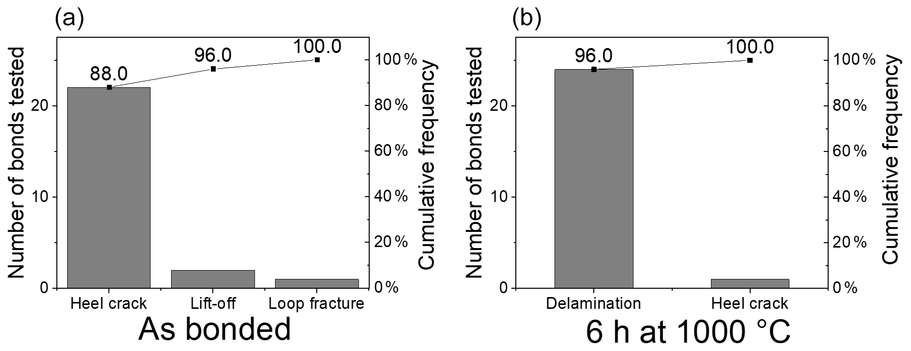
Figure 10Frequency of failure mechanisms of wire bonds, for different ageing conditions, bonded to thin film. (a) No annealing and (b) aged for 6 h at 1000 ∘C.
It is apparent that ageing of the bonds changes the failure mode (Fig. 10). Heel crack defines the fracture in the transition area between wedge (deformed area of the wire) and the unprocessed wire. Delamination is defined as the detachment of the platinum layer from the sapphire substrate with the bond. In the tested samples, the heel crack occurs in 88 % of the specimens without ageing. The failure mode changes to over 90 % delamination due to thermal ageing. This indicates a loss of the adhesive strength of the metallisation on the sapphire. The delamination is also visible in Fig. 8. Here, the entire thin layer, i.e. titanium and platinum, is detached from the substrate. The enlarged area on the right in Fig. 8 shows the bare sapphire at the bond base after the wire pull test. It can be concluded that the bond strength of the thin film metallisation after thermal ageing is the limiting factor for the bond strength in pull-off tests.
The wire pull force for the thick film wire bonds has a mean value of 70 mN before thermal ageing. It can be seen that thermal ageing initially leads to an increase in wire pull forces. An ageing of 6 and 12 h at 1000 ∘C increases the measured forces equally by 40 % to a mean value of 98 mN. After ageing for 24 h at 1000 ∘C, the mean wire pull force is reduced to 79 mN but remains higher than the original ones measured before thermal ageing.
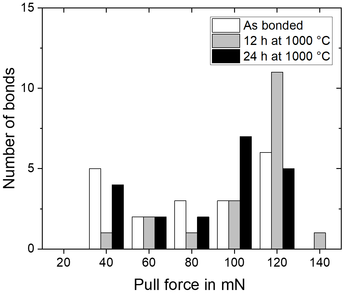
Figure 11Bond strength distribution on a platinum thick film layer on sapphire, as bonded and after the thermal ageing of the bond on thick film for 12 h at 1000 ∘C and 24 h 1000 ∘C.
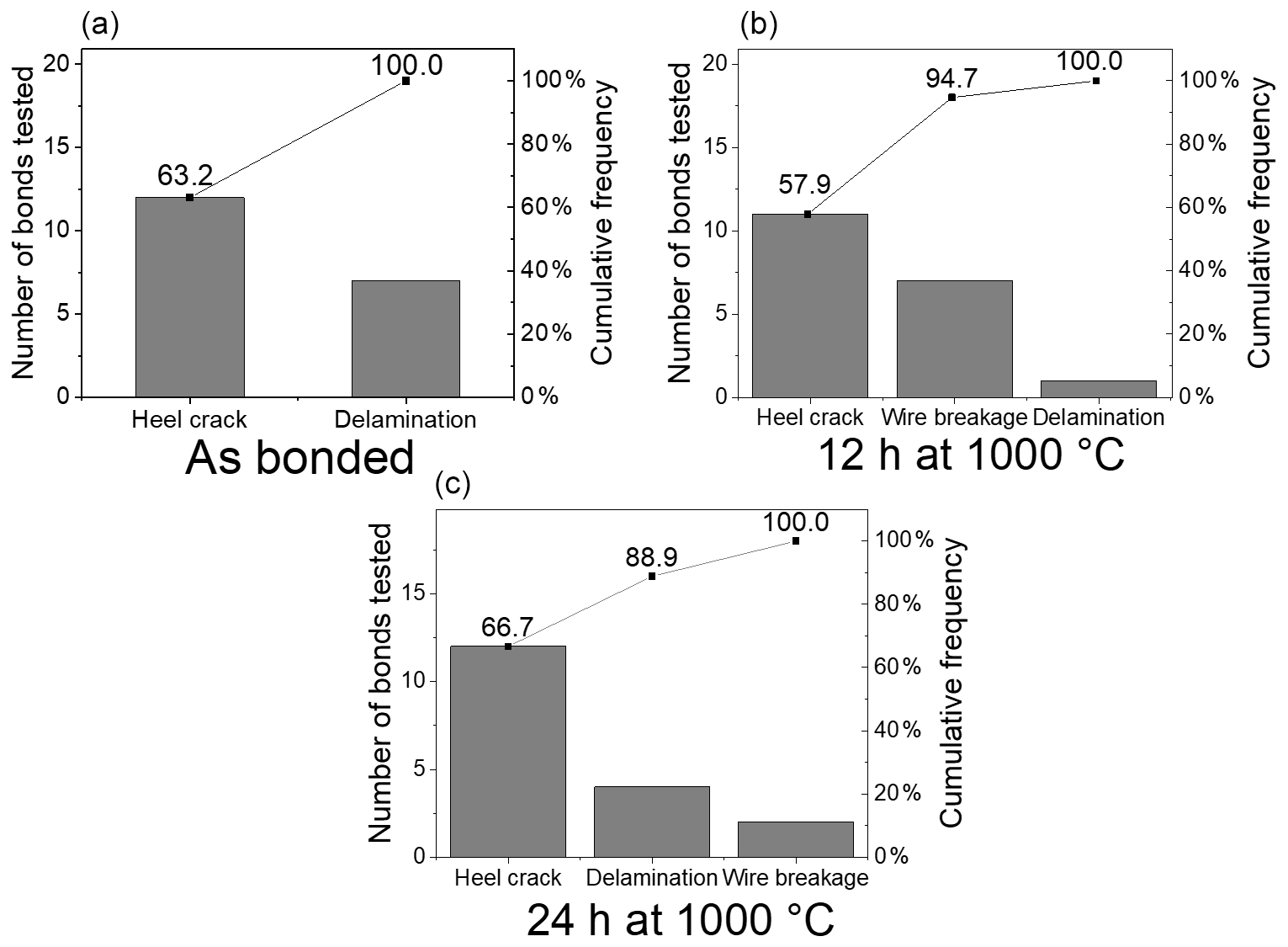
Figure 12Frequency of the failure mechanisms of wire bonds, for different ageing conditions, bonded to thick film. (a) No annealing, (b) aged for 12 h at 1000 ∘C, and (c) aged for 24 h at 1000 ∘C.
Before thermal ageing, the failure mechanism of delamination or bond lift (37 %) and heel crack (63 %) is predominant (Fig. 12).
After thermal ageing, the occurrence of delamination or bond lift decreases from 37 % to 5 %, and failure via heel cracks initially reduces from 63 % to 58 %. A shift of the predominant failure mechanism towards wire fracture can be observed.
Therefore, the thick film wire bond is evaluated as being more thermally stable but can still be improved by further thick film surface optimisation and bond parameter adjustment.
3.3 Metallographic view of the connections
The cut through the bond base in Fig. 13 shows the transition area of the platinum from the bond base to the metallisation. The thin film section shows the punctual bonding of the bond base with the platinum metallisation.
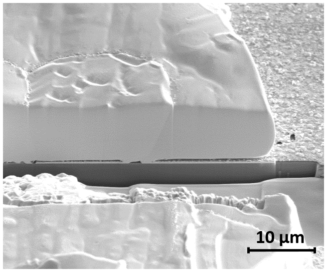
Figure 13The focused ion beam (FIB) cut through the centre of a wire bond on thin film platinum metallisation.
The thick film section (Fig. 14) also reveals smaller areas of punctual bonding.
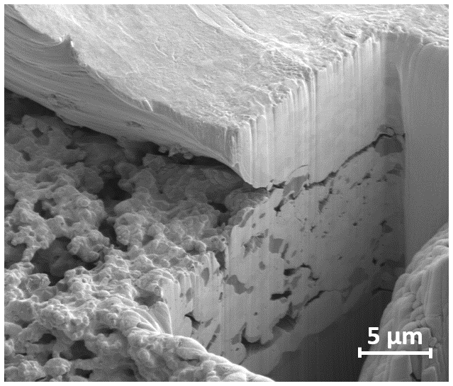
The platinum thick film layer, which was thermally aged before the bonding process, exhibits pores. These make reproducible bonding difficult. Due to the rather rough surface of the thick film, more surface of the joining partners is in contact. It can be seen in Fig. 14 that the bond foot adapts to the geometry of the thick film.
The relationship between the bonding force and ultrasonic power determined here shows the best results for the platinum thick film layer examined. Higher bonding forces and higher ultrasonic power sometimes led to layer breakdown. The subsequent thermal ageing has led to an improvement in the layer quality and to better bondability of the thick film layers. Depending on all process parameters during the firing of the thick film (e.g. maximum firing temperature and ageing time), further adjustment of the bonding parameters should therefore be considered.
In this work, the thick film technique is pursued further due to its lower tendency to delaminate from sapphire at higher temperature. In future investigations, more densified platinum layers are to be used for long-term temperature-resistant bonds.
3.4 Glass solder joining
The results in Fig. 15 show that, on the back side of the sapphire surface (roughness Sa = 1.5 µm), an average shear strength of 50 MPa can be measured.
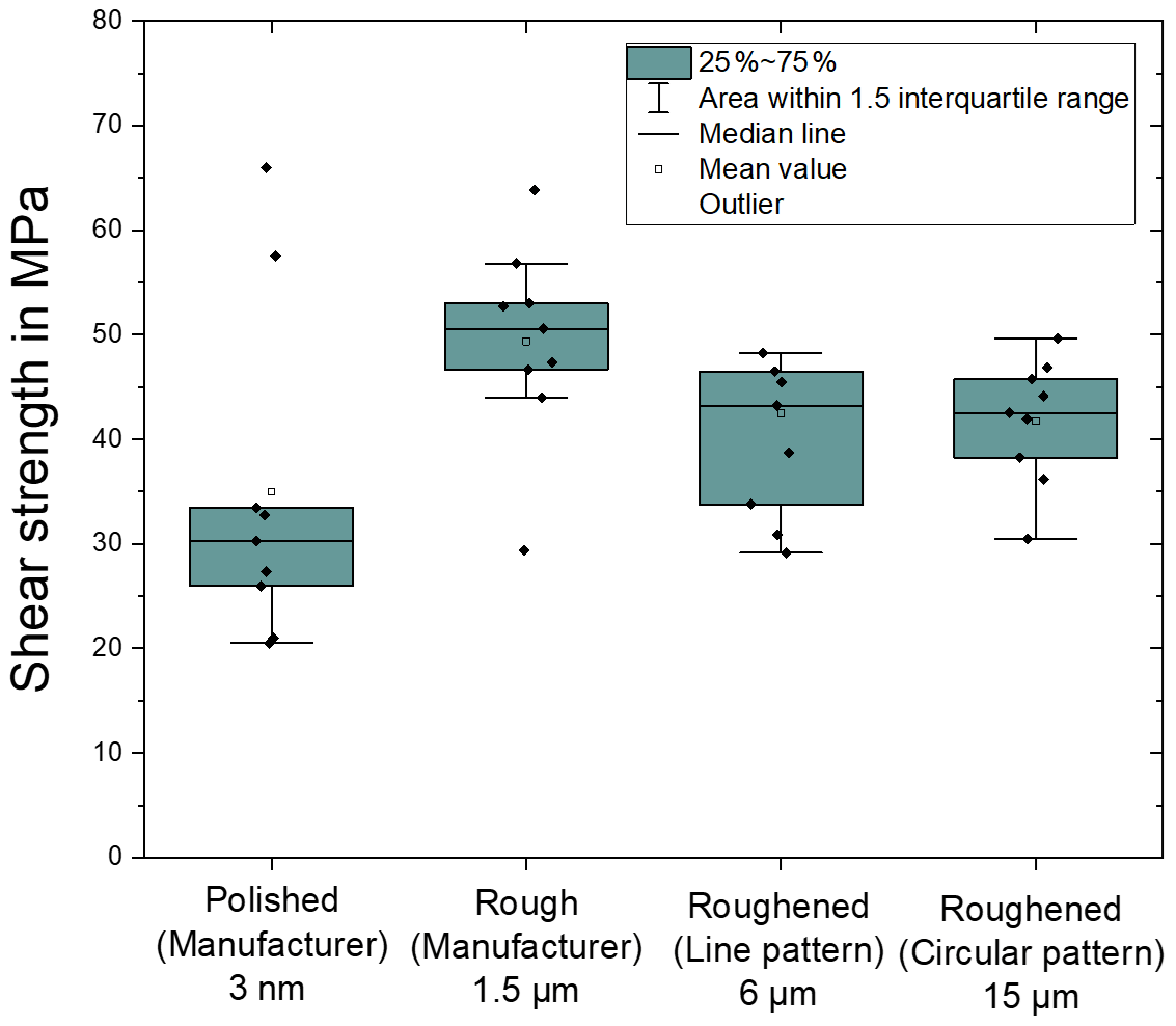
Figure 15Shear strength of glass-soldered Al2O3 chips on differently structured sapphire substrates. Glass solder G018-385 and sample size n=9.
An increase in roughness by laser structuring does not yield better shear strength. Both the line pattern and the circular pattern exhibit a shear strength of approximately 42 MPa. Very smooth, polished surfaces lead to only 30 MPa. This indicates that mechanical interlocking and an increase in the effective bond area have strong effects. As the glass solder has a viscosity of 1000 Pa s at 962 ∘C, it can flow well. Figure 16 shows that this allows the rough surface of the sapphire to be wetted and filled.
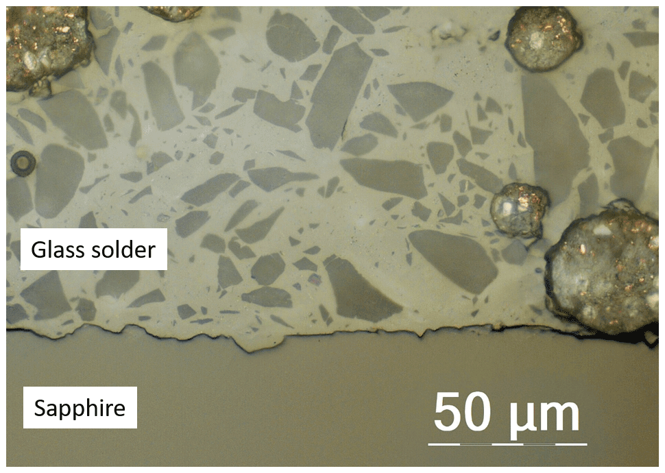
Figure 16Cross section of glass solder on rough sapphire backside, with a surface roughness of Sa = 1.5 µm (sapphire).
In Fig. 16, air inclusions can be seen in the zone of the glass solder. To avoid these, the glass solder paste was stored in a vacuum atmosphere. In addition, different weights were applied to the shear test samples. In this way, the complete oven process of the glass solder can be realised under pressure.
By applying a pressure of 0.55 MPa on the 2 mm × 2 mm chip, the average shear strength can be increased from 50 to about 85 MPa (Fig. 17). A similar tendency is also seen for the minimum strength, which increases from 25 to 50 MPa. The effect of the bonding force/pressure is significant. It can be explained by the reduction in the bond layer thickness and the avoidance of air inclusions.

Figure 17Shear strength of glass-soldered Al2O3 chips under pressure. Glass solder G018-385 and sample size n=9 per pressure.
The good shear strength is partly maintained after thermal ageing. A box plot with a median line and a range of the 1.5 interquartile shows the trend during thermal ageing (Fig. 18). The cause of this decrease is still open. Nevertheless, shear strengths in the range of 50 MPa are still achieved even after 12 and 24 h exposure to temperature of 1000 ∘C. Further tests will show whether this value range can also be maintained for longer temperature loads at 1000 ∘C.

Figure 18Influence of heat treatment on the shear strength. Glass-soldered chips under 0.55 MPa pressure and sample size n=9.
3.5 Electrical characterisation of the package
For a reliable sensor concept with good signal quality, it is important to know properties such as the electrical conductivity and the insulation resistance of its materials. Most insulators tend to become intrinsic (semi-)conductors at temperatures above 500 ∘C. This effect contributes to so-called electrical parasitics that degrade the performance of resonance sensors. To account for such phenomena, electrical measurements are made on the assembly materials.
3.5.1 LCR measurements on sapphire
The interdigital structure, shown in Fig. 3, exhibits a capacitance of 652 nF at room temperature (21 ∘C) at a frequency of 2 MHz. It increases to 745 nF at 1000 ∘C. The dissipation factor rises from 0.028 at room temperature to 0.072 at 500 ∘C and to 0.23 at 1000 ∘C. It can also be seen that the increase of the dissipation factor is degressive at higher temperature.
Figure 19 shows that the dissipation factor for the highest frequency of 2 MHz at 1000 ∘C is lower compared to frequencies of 1 and 500 kHz.
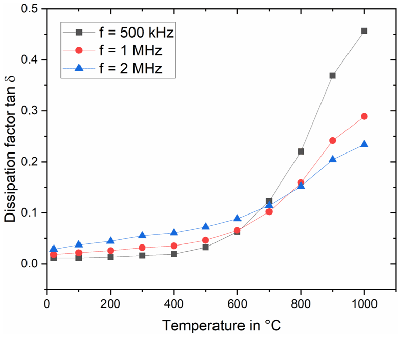
Figure 19Dissipation factor, tan δ, measured as a function of temperature and frequency up to 1000 ∘C.
Table 5Calculated permittivity εr at 2 MHz of sapphire up to 1000 ∘C for different thin film interdigital structures, with 30, 40, and 50 µm width and spacing.
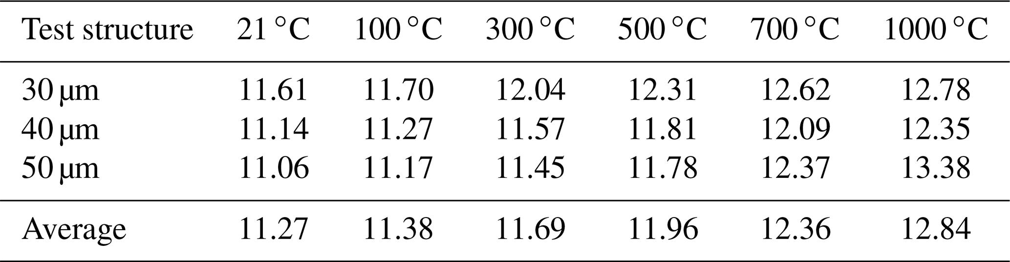
The measurements were performed on interdigital structures with different finger widths and finger spacings. Using the capacitance data, a value for the relative permittivity can then be calculated using the formula in Eq. (1). Permittivity values calculated from the capacitance values at 2 MHz are given in Table 5.
The measured value of εr = 11.27 at room temperature is similar to the literature value of 11.5 for sapphire (Dobrovinskaya, 2009). In addition, the trend towards higher values at higher temperature becomes clear. At 1000 ∘C, the relative permittivity reaches a value of 12.8. This indicates the weak dependency of the measured relative permittivity of the sapphire over the wide temperature range.
3.5.2 Dielectric properties of the glass solder
For the dielectric characterisation of the glass solder, the interdigital structure is coated with the same process as for the glass soldering. The resulting layer thickness is 70 µm. The capacitance is recorded using the LCR meter. Figures 20 and 21 show the capacitance and the dissipation factor over the temperature range.

Figure 20Capacitance of the test structure (Fig. 3), with and without glass solder, up to 1000 ∘C.
The capacitance of the glass-coated interdigital structures shows a stronger increase than that of the uncoated one.
By measuring the same comb structure with and without a glass solder coating, the relative permittivity of the glass solder can be calculated via the partial components of the total capacitive value (Eq. 2). The derived value of the relative permittivity of the glass increases from εr = 5 at room temperature to εr = 14 at 1000 ∘C and 2 MHz.
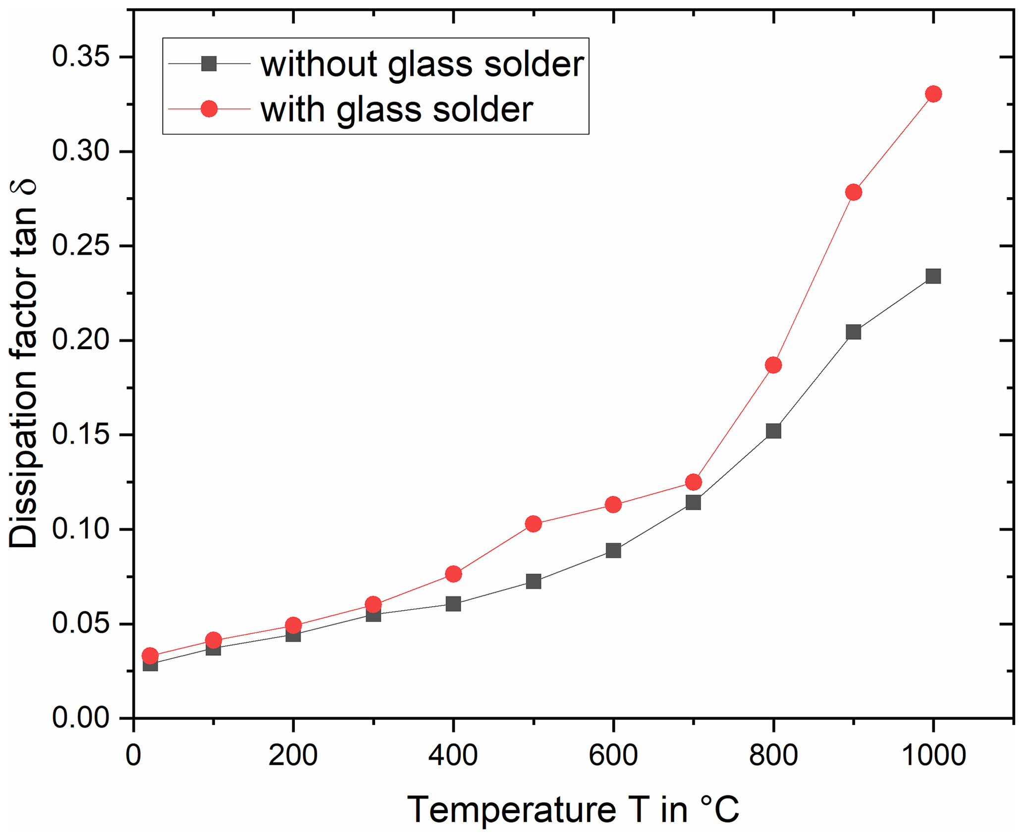
The dissipation factor in Fig. 21 shows similar values for the specimen with and without glass solder coating in the temperature range below 700 ∘C. Above this temperature, the loss factor increases more for the specimen with glass solder. This suggests an increase in conductivity in this temperature range.
To obtain further information on the behaviour of the conductivity, direct current (DC) measurements are performed on both the sapphire substrate and the glass solder material, with plate structures between 400 and 1000 ∘C.
The measured values in Fig. 22 show an increase in conductivity with temperature for both materials. The conductivity of the sapphire substrate increases from 9.8 × 10⁻¹⁰ S m−1 at 400 ∘C to 5.3 × 10⁻⁷ S m−1 at 900 ∘C. The increase in the conductivity of the glass solder is from 7.2 × 10⁻¹⁰ S m−1 at 400 ∘C to 8.9 × 10⁻³ S m−1 at 900 ∘C.

Figure 22Measured conductivity using the plate structure with sapphire and glass solder insulating material as a function of temperature.
Table 6Helium leak rates over the time of thermal ageing at 1000 ∘C.
By thermal activation, significant differences in the conductivity of the two materials are observed. This can be attributed to the generation of carriers and, thus, to a higher intrinsic conductivity of the glass solder. The multi-material glass has more cations, vacancies, grain boundaries, and dislocations, which can lead to higher conductivity compared to the single crystal form of the sapphire.
The loss factor for AC measurement is made up of the rearrangement losses and the conductivity. If the conductivity increases, the loss factor also increases.
The result of the DC measurement is consistent with the AC measurement (Fig. 21), since the dissipation factor of the coated comb structure increases above 700 ∘C, which can be attributed to a higher conductivity.
3.6 Hermeticity analysis
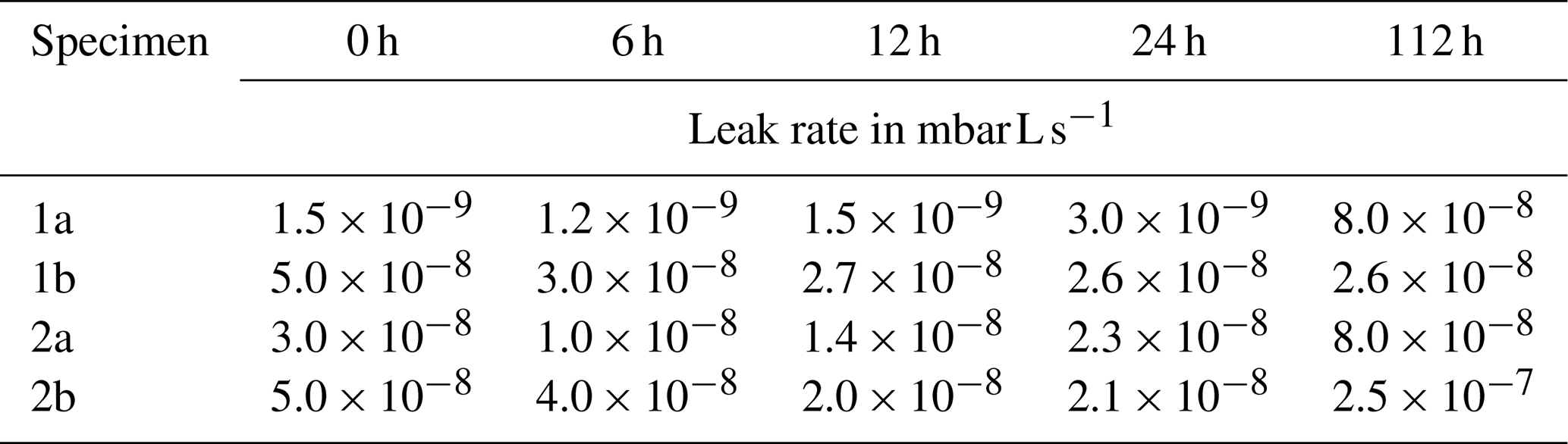
Hermeticity was tested with helium leak tests. Table 6 shows the helium leak rate of the package where the ceramic cap was attached to the sapphire substrate with glass solder. Specimens 1a and 1b represent the assembly with a closed hole in the sapphire and 2a and 2b with a closed hole in the cap (Fig. 1). The packages underwent thermal ageing at 1000 ∘C for up to 112 h.
The measurements of the housings in Table 5 show values in the range of 10−8 mbar L s−1 without thermal ageing. This range of values can also be mostly maintained over the thermal load at 1000 ∘C for 112 h. Furthermore, no significant differences can be seen due to the subsequent closure of the hole in the sapphire or in the Al2O3 encapsulation lid.
The increase in the leakage rate of Specimen 2b should be further observed in the course of the ageing process in order to exclude a failure of the glass solder connection. With an overpressure of 1 bar, this would result in a gas loss of 1 cm3 in 110 d. The classification in the case of a leakage rate in the range of 10−7mbar L s−1 can be considered as being gas tight.
These results enabled the realisation of a gas-tight and temperature-stable design for a piezoelectric temperature sensor for temperatures up to 1000 ∘C.
3.6.1 Influences on the sensor behaviour
With the packaging technology, a housed temperature sensor was built up (Fig. 23). An unhoused sensor Shanghai Institute of Ceramics, Chinese Academy of Sciences (SICCAS) serves as a comparison.
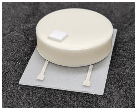
Figure 23Realised sensor housing for the piezoelectric CTGS resonator as a temperature sensor.
A comparison of the Q factor shows nearly no differences between the housed and unhoused sensors in the lower temperature range (< 500 ∘C; Schulz et al., 2021).
Table 7Inverse Q factor of unhoused CTGS specimen and housed CTGS specimen (Schulz et al., 2021).
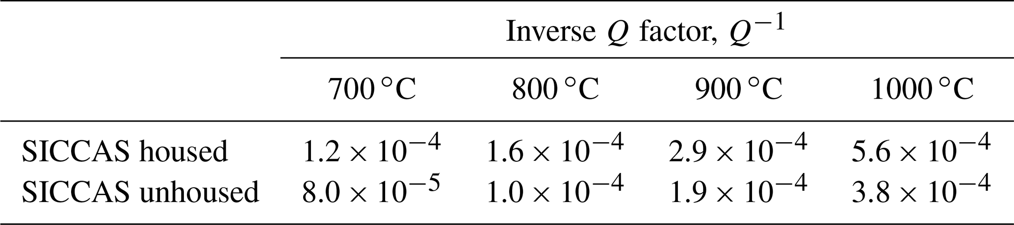
These Q factors of the housed and unhoused sensors are of the same order of magnitude. In the measured range from 700 to 1000 ∘C the housed sensor has slightly higher inverse Q factors compared to the unhoused one (Table 7).
Consequently, the housing concept has only a limited influence on the performance of the CTGS resonator in the sensor concept presented. The quality factors show that the sensor continues to perform well, even with the housing. So, the design concept should provide a solid basis for further sensor designs.
This work has shown the possibility of assembly and interconnection technology for use under high temperatures up to 1000 ∘C. A packaging concept was developed, and all the necessary material and joining technologies have been verified to be suitable for use at 1000 ∘C. The adhesion strength of thick films and thin films after thermal ageing, as well as the tensile strength of wire bonds after thermal load, were investigated. A better temperature resilience of the thick film metallisation compared to the thin film metallisation is shown. Furthermore, investigations were carried out with glass solder on differently structured sapphire surfaces. The influence of the pressure parameter during curing of the glass solder was examined in more detail. The results show good shear strengths after temperature loads. The thermal ageing suggests a progression to a stable limit of shear strength.
The electrical measurements provide information about the relative permittivity of the sapphire substrate. These values show that the material still has good insulation properties at high temperature such as 1000 ∘C and are comparable with the literature values (Dobrovinskaya et al., 2009). Furthermore, a measurement of the capacitance of glass solder up to 1000 ∘C temperature could be performed. With these measured values, the relative permittivity of the glass solder and sapphire can be calculated. The glass solder shows a higher value of the loss factor at higher temperature. This suggests an increase in the conductivity of this material. The conductivity of both materials in the temperature range up to 1000 ∘C could be determined via direct current measurement. The results show a higher increase in conductivity of the multi-material glass solder material compared with the single-crystalline sapphire. Influences on the sensor signal can be further analysed by manufacturing and comparing additional prototypes of the sensor housing.
The helium leak test showed that the presented assembly concept is also gas tight over an ageing period of 112 h at 1000 ∘C.
The assembled prototype package includes a sapphire substrate with thick film traces. The sensor is interconnected with platinum wires with a diameter of 25 µm. The housing lid and spacer made of multi-crystalline alumina are attached with glass solder.
A working sensor was built and measured in comparison to the resonator alone. To explain the rather small differences, all package materials and structures were measured electrically and dielectrically. As a result, equivalent circuits for the packages up to 2 MHz and 1000 ∘C are available. The housing shows no significant influence on the performance of the sensor with regard to the Q factor. In a parallel paper, the results of the thermal behaviour of the device as a temperature are presented (Schulz et al., 2021).
The assembly and packaging technology provides a platform for other properties to be measured, such as pressure or chemical composition, at very high temperature. Further prototypes for other physical parameters are already planned.
The data presented in this article are stored in an internal system according to the guidelines of the DFG. Research data are available upon request to the authors.
FK and MF were responsible for the bonding and assembly of complete devices. MS was responsible for the preparation and characterisation of CTGS resonators. FK and MF performed the experiments on the assembly and interconnection components, analysed the data, and wrote initial paper. HF and JW initiated the research project and supported FK and MS with data interpretation and discussion. JW and HF revised the paper and led the project. FK and JW approved the final version of the paper.
The contact author has declared that neither they nor their co-authors have any competing interests.
Publisher's note: Copernicus Publications remains neutral with regard to jurisdictional claims in published maps and institutional affiliations.
This research has been supported by the Deutsche Forschungsgemeinschaft (grant nos. WI1987/6-1 and FR 1301/35-1).
This open-access publication was funded by the University of Freiburg.
This paper was edited by Mervi Paulasto-Kröckel and reviewed by two anonymous referees.
Alley, G.: Interdigital capacitors and their application to lumped-element microwave integrated circuits, IEEE T. Microwave Theory Tech., MTT-18, 12, https://doi.org/10.1109/TMTT.1970.1127407, 1970.
Bahl, I.: Lumped elements for RF and microwave circuits, Artech House, ISBN 978-1580533096, 2003.
Bernhardt, G., Silvestre, C., Lecursi, N., Moulzolf, s. c., Frankel D. J., and Lad, R. J.: Performance of Zr and Ti adhesion layers for bonding of platinum metallization to sapphire substrates, Sensor. Actuat. B-Chem., 77, 368–374, 2001.
Damjanovic, D.: Materials for high temperature piezoelectric transducers, Curr. Opin. Solid St. M., 3, 469–473, https://doi.org/10.1016/j.proeng.2016.11.322, 1998.
Department of defense test method standard: Microcircuits, https://www.jedec.org/taxonomy/term/2754, last access: 18 March 2022.
Dobrovinskaya, E. R., Lytvynov L. A., and Pishchik V.: Sapphire; Material, Manufacturing, Applications, in: Micro- and opto-electronic materials, structures, and systems, Springer, https://doi.org/10.1007/978-0-387-85695-7, 2009.
Farina, M.: Vergleich von Platinmetallisierungen zur Evaluierung von Saphireigenschaften und Platindrahtbonds als Teil eines Aufbaukonzepts für einen BAW-Sensor bis 1000 ∘C, MS thesis, University of Freiburg, Freiburg, https://freidok.uni-freiburg.de/data/225620 (last access: 21 March 2022), 2021.
Fritze, H., Schneider, O., She, H., Tuller, H. L., and Borchardt G.: High temperature bulk acoustic wave properties of langasite, Phys. Chem. Chem. Phys., 5, 5207–5214, https://doi.org/10.1039/B307503F, 2003.
Fu, X., Noguchi, Y., Matsushita, M., and Miyayama, M.: Influence of growth conditions on the optical, electrical resistivity and piezoelectric properties of Ca3TaGa3Si2O14 single crystals, J. Ceram. Soc. Jpn., 124, 523–527, https://doi.org/10.2109/jcersj2.15293, 2016.
Gevorgian, S., Martinsson, T., Linner, P., and Kollberg, E.: Cad models for multilayered substrate interdigital capacitors, IEEE T. Microw. Theory, 44, 896–904, 1996.
Hassanin, H.: Fabrication of ceramic and ceramic composite microcomponents using soft lithography, PhD thesis, University of Birmingham, Birmingham, https://doi.org/10.1533/9780857098825.3.611, 2011.
Knechtel, R., Wiemer, M., and Frömel, J.: Wafer level encapsulation of microsystems using glass frit bonding, Microsyst. Technol., 12, 468–472, https://doi.org/10.1007/s00542-005-0036-4, 2006.
Lv, Y., Han, Y., Zhao, S., Du, Z., and Fan, J.: Nano-in-situ-composite ultrafine-grained W–Y2O3 materials: Microstructure, mechanical properties and high heat load performances, J. Alloy. Compd., 855, 157366, https://doi.org/10.1016/j.jallcom.2020.157366, 2021.
Oezkan, O. and Moulson, A.: The electrical conductivity of single-crystal and polycrystalline aluminium oxide, J. Phys. D Appl. Phys., 3, 983–987, https://doi.org/10.1088/0022-3727/3/6/420, 1970.
Schulz, M., Ghanavati, R., Kohler, F., Wilde, J., and Fritze, H.: High-temperature behavior of housed piezoelectric resonators based on CTGS, J. Sens. Sens. Syst., 10, 271–279, https://doi.org/10.5194/jsss-10-271-2021, 2021.
Seifert, M., Brachmann, E., Rane, G, Menzel, S., and Gemming, T.: Capability study of Ti, Cr, W, Ta and Pt as seed layers for electrodeposited platinum films on γ-Al2O3 for high temperature and harsh environment applications, MDPI Materials, 10, 54, https://doi.org/10.3390/ma10010054, 2017.
Subbiah, N., Ramirez, K., Wilde, J., and Bruckner, G.: Concept and Implementation of High-Temperature Pressure Sensor Package up to 500 ∘C, Sensoren und Messsysteme, VDE Verlag GMBH, ISBN 978-3-8007-4683-5, 2018.
Suhak, Y., Schulz, M., Johnson, W. L., Sotnikov, A., Schmidt, H., and Fritze, H.: Electromechanical properties and charge transport of Ca3TaGa3Si2O14 (CTGS) single crystals at elevated temperatures, Solid State Ionics, 317, 221–228, 2018.
Tyagi, A. and Banerjee, S. (Eds.): Materials Under Extreme Conditions, Chapter 6: Glasses and Glass-Ceramics, Elsevier Science Publishing Co Inc., ISBN 978-0-12-801300-7, 2017.
Yu, F., Zhang, S., Zhao, X., Yuan, D., Qin, L.,Wang, Q., and Shrout, T. R.: Investigation of Ca3TaGa3Si2O14 piezoelectric crystals for high temperature sensors, J. Appl. Phys., 109, 114103, https://doi.org/10.1063/1.3592347, 2011.
Zang, L. J., Sharif, A., Yeung, H. B., Rong, E. P. J., Riko, I. M., Long, L. F., Dy, L. J., and Cheong, W. C.: Ceramic – ceramic joining using glass frit for high temperature application, in: IEEE 14th Electronics Packaging Technology Conference (EPTC), 5–7 December 2012, Singapore, https://doi.org/10.1109/EPTC.2012.6507047, 2012.
Zeiser, Z.: Mikromechanische Drucksensoren mit spezifischer Aufbautechnik für den Einsatz bei 500 ∘C, dissertation, University of Freiburg, Freiburg, https://freidok.uni-freiburg.de/data/225632 (last access: 22 March 2022), 2015.
Zeitouny, Z.: Analysis of high temperature enclosure concepts for sensors up to 1000 ∘C, MS thesis, University of Freiburg, Freiburg, https://freidok.uni-freiburg.de/data/225621 (last access: 21 March 2022), 2021.