the Creative Commons Attribution 4.0 License.
the Creative Commons Attribution 4.0 License.
 | 22 May 2024
Optical and tactile measurements on SiC sample defects
Bernd Bodermann
Elena Ermilova
Matthias Weise
Andreas Hertwig
Petr Klapetek
Jila Rafighdoost
Silvania F. Pereira
In power electronics, compound semiconductors with large bandgaps, like silicon carbide (SiC), are increasingly being used as material instead of silicon. They have a lot of advantages over silicon but are also intolerant of nanoscale material defects, so that a defect inspection with high accuracy is needed. The different defect types on SiC samples are measured with various measurement methods, including optical and tactile methods. The defect types investigated include carrots, particles, polytype inclusions and threading dislocations, and they are analysed with imaging ellipsometry, coherent Fourier scatterometry (CFS), white light interference microscopy (WLIM) and atomic force microscopy (AFM). These different measurement methods are used to investigate which method is most sensitive for which type of defect to be able to use the measurement methods more effectively. It is important to be able to identify the defects to classify them as critical or non-critical for the functionality of the end product. Once these investigations have been completed, the measurement systems can be optimally distributed to the relevant defects in further work to realize a hybrid analysis of the defects. In addition to the identification and classification of defects, such a future hybrid analysis could also include characterizations, e.g. further evaluation of ellipsometric data by using numerical simulations.
- Article
(8518 KB) - Full-text XML
- BibTeX
- EndNote


Power electronic components are used in many areas of application in our daily lives. They are needed for intelligent power distribution, electromobility, and 5G communication. Currently, power electronics is still dominated by silicon as a material. However, there is an increasing shift from silicon to compound semiconductors with large bandgaps. Silicon carbide (SiC), for example, is one such compound semiconductor. The advantages over silicon are that they can operate at higher frequencies, temperatures, and voltages. In addition, the final products are smaller and lighter, so there is less energy loss. However, during the manufacturing process, defects arise which negatively influence the functionality of the end product and which are the cause of yield enhancement still being a grand challenge (Wilson et al., 2021). Therefore, defect inspection with high sensitivity is required for these materials (Wilson et al., 2021; Treu et al., 2012; Alves et al., 2017).
Defects on SiC have different causes. A general distinction is made between crystallographic defects in the wafer and surface defects. Crystallographic defects and impurities can extend onto the wafer surface during growth and form surface defects (Chen et al., 2022).
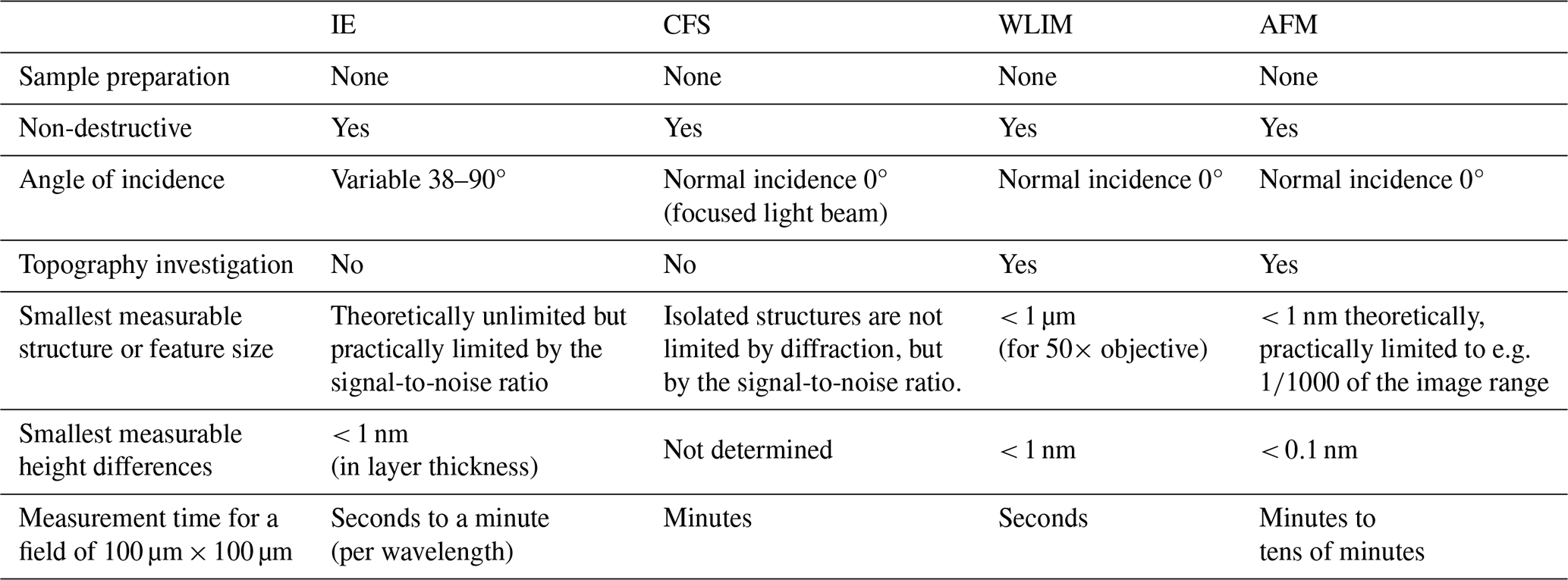
There already exist many established defect inspection methods. The aim here is to investigate further methods that use ellipsometric and scatterometric measurements to supplement a degree of polarization freedom to obtain different and increased sensitivities in relation to the defect geometries compared to conventional methods. A further advantage of these methods is that there is no principal lower limit on the size of measurable structures or features. Unlike microscopic methods, which as image-based methods are fundamentally limited by their resolution (Abbe limit), scattered light methods have the capability to characterize structures that are orders of magnitude smaller than the used optical wavelength and also the used interaction range. Imaging ellipsometry (IE) and also coherent Fourier scatterometry (CFS) combine all these advantages. Imaging ellipsometry is applied here to significantly reduce the analysed interaction area, which allows us to characterize small individual features and which has significant advantages in the signal-to-noise ratio for sparse defect surfaces. Atomic force microscopy (AFM) and white light interference microscopy (WLIM) measurements are used to determine the topography of the defects to obtain initial approaches for later simulations.
For each of these four measurement methods, it will be determined for which defect types they are most sensitive so that the devices can be used optimally. In further work, these can then be used not only to detect the defects but also to characterize them.
The SiC epitaxial wafers used for the measurements were grown in an AIXTRON multi-wafer production-type chemical vapour deposition (CVD) reactor.
The samples investigated here are homoepitaxial 12 µm 4H-SiC layers on 4H-SiC (n+ (nitrogen-doped) 4H polytype cut at 4°) substrates. The most common defects of the SiC samples measured here are shown as microscope images in Fig. 1 and as an AFM image in Fig. 7c. These are so-called carrot defects, polytype inclusions, particles, and threading dislocations. The defects in SiC are typically divided into two groups: crystallographic defects in the wafer and surface defects. Carrot defects and polytype inclusions belong to surface defects, whereas particles and dislocations belong to crystallographic defects. Particle inclusions are generated by falling particles during the growth process. They can be reduced by manufacturing under clean and controlled conditions (Chen et al., 2022).
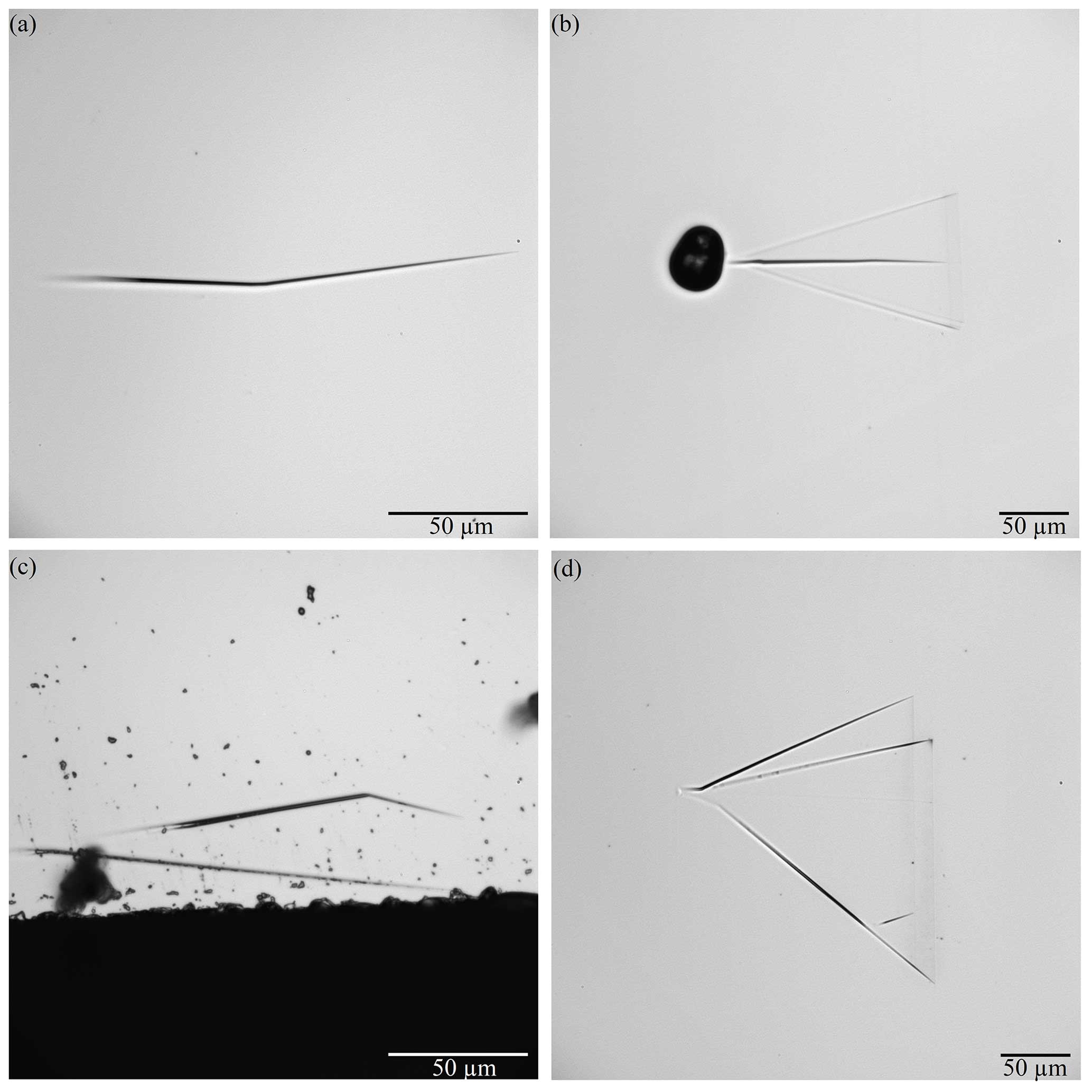
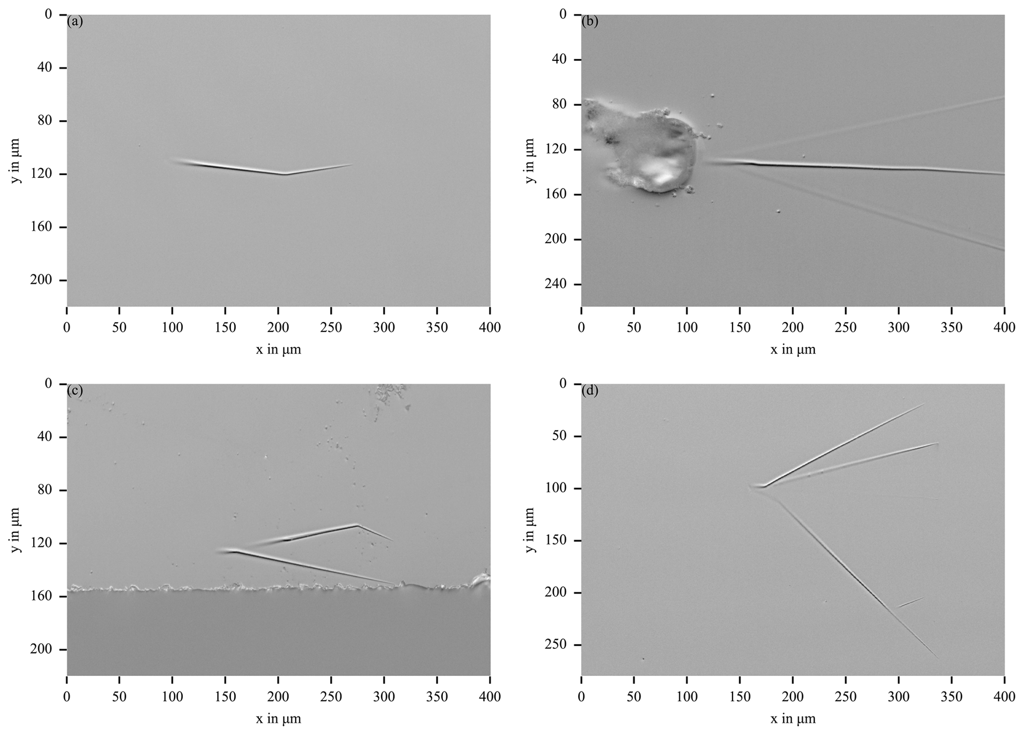
Figure 1Microscopic images of the defects under estimation, captured with a normal incidence microscope at a wavelength of 500 nm: (a) carrot, 20× objective with numerical aperture NA = 0.5; (b) polytype inclusion with particle, 10× objective with NA = 0.3; (c) carrot, 20× objective with NA = 0.5; and (d) polytype inclusion, 10× objective with NA = 0.3.
2.1 Investigated defect types
Dislocations can appear as so-called threading or basal plane dislocations. They occur on 4H-SiC substrates with densities between 103 and 104 cm−2. They are responsible for reducing the minority carrier lifetime, increasing the leakage current and causing reliability problems of the final products. During homoepitaxy, dislocations either propagate into the epitaxial layer (more than 95 %) or convert to other dislocation types. The dislocations are formed due to thermal or steric stress during the growth of 4H-SiC single crystals (Li et al., 2022b).
Threading dislocations show up on the surface as etch pits with different shapes and dimensions, so that they can be further divided into threading edge, threading screw, and threading mixed dislocations. In a cross-sectional view, threading mixed dislocations are characterized by a conical shape, threading screw dislocations have a triangular cross section, and threading edge dislocations (TEDs) have an arc-shaped cross section (Yu et al., 2021).
Especially in the case of TEDs, due to the small dimensions in the micrometre-to-sub-micrometre regime (in both width and depth), imaging with conventional optical measurement methods no longer allows us to characterize sub-micron defect details, and for this purpose tactile measurement methods are required instead.
Surface defects can occur if crystallographic defects and impurities spread to the homoepitaxial wafer surface during growth. Carrot defects are among the most common surface defects and are responsible for increasing the reverse leakage current of 4H-SiC Schottky and p–n junction diodes (Zhao, 2020). Various studies have been conducted on the structure and cause of carrot defects. According to Benamara et al. (2005), the defects consist of two intersecting planar faults on prismatic and basal planes, with the two connected by a stair-rod dislocation. The cause of this surface defect is a threading screw dislocation in the wafer, according to the authors. Hassan et al. (2010) have investigated various carrot defects and were able to trace each of the structures back to the model of Benamara et al. (2005) They have also found further causes of the carrot defects, such as basal plane dislocations, threading screw dislocation stacking faults, or dislocation slip bands, and even substrate surface damage can be a cause of these defects. The surface morphology of the defect depends on the composition of the respective defect.
Polytype inclusions, or triangle defects, are also among the most common surface defects on 4H-SiC epitaxial layers. They have a negative impact on the reliability of the product and are therefore also called killer defects. Two well-known models exist of the origin of these defects, which agree that they are 3C-SiC nucleation on off-axis 4H-SiC substrates (Guo et al., 2017). Only the cause of this nucleation is reasoned differently. Konstantinov et al. (1997) and Hallin et al. (1997) assume that these defects originate from substrate imperfections. Polytype inclusions, according to them, form large on-axis terraces with a large supersaturation originating from spontaneous two-dimensional nucleation and growth from the triangle apex. Si et al. (1997) explain that the cause of 3C nucleation is step bunching during epitaxial growth. According to these authors, with a sufficiently large step period, supersaturation can be achieved at the terrace sufficient to initiate two-dimensional nucleation, which in turn leads to the formation of 3C-SiC.
Polytype inclusions have different morphologies, so that they can be divided into three types (Guo et al., 2017). Type A is characterized by a large particle at the top of the defect. The attached triangular shape is divided into a smooth surface and a rough surface. The smooth surface is a 3C layer overgrown by 4H-SiC steps and the rough surface is a 3C layer that is not overgrown. Type B usually has a smaller particle than type A at the top and the entire surface is overgrown by macro steps of 4H-SiC that create a rough surface. Type-C defects have a smoother surface than type-B defects, suggesting that the growth steps are much finer (Guo et al., 2017).
Accordingly, the polytype inclusion in Fig. 1b is a combination of types A and C due to the large particle and smooth surface and, in Fig. 1d, a type-C defect. Both defects have an area without 4H overgrowth represented by a line within the triangle.
2.2 Inspection methods: state of the art
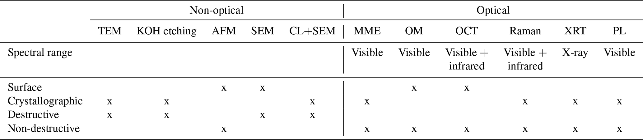
There are already various defect inspection methods for SiC in use. These include optical and non-optical methods, which differ again in whether they can examine the surface defects or the crystallographic defects. Widely used methods of non-optical defect inspection are transmission electron microscopy (TEM) and KOH etching. Both methods examine the crystallographic defects, but they cause irreversible damage to the samples and are therefore not suitable for in-line use. Other measurement systems for the non-optical case are AFM, scanning electron microscopy (SEM) or cathodoluminescence (CL) in combination with SEM. However, these methods have the disadvantage that they have extended measurement times. Another method that is already in use is non-imaging Mueller matrix ellipsometry (MME). This can be used to examine crystallographic defects, whereby indications of the examined defects can be found, particularly in some off-diagonal elements of the Mueller matrix (Li et al., 2022a). Optical measurement systems for defect inspection include optical microscopy (OM) and optical coherence tomography (OCT), which perform measurements of surface defects. Raman spectroscopy, X-ray diffraction topography (XRT), and photoluminescence (PL) can examine crystallographic defects. However, OCT has a comparatively low inspection speed and resolution, while Raman measurements are relatively slow (Chen et al., 2022).
For a summarized overview of the mentioned measurement methods, refer to Table 1.
3.1 Imaging ellipsometry
Ellipsometry is an optical measurement method in which the change in the polarization state of light is analysed after interaction with the sample. In this way, conclusions can be drawn about the dielectric properties of film layers or about the layer thickness of thin films. It is an indirect measurement method, so numerical simulations are needed to solve Maxwell's equations and the inverse problem (Azzam and Bashara, 1977). In ellipsometry, only relative phase and amplitude measurements are performed, and therefore it is a very accurate measurement method (Losurdo and Hingerl, 2013; Goldstein, 2003; Chipman, 1994). The polarization of the emitted light is determined by a polarization state generator (PSG). The light then hits the sample and is reflected by it or transmitted through it, whereupon it reaches a polarization state analyser (PSA) where it is analysed with respect to its polarization. Finally, a detector measures the intensity of the light. The PSG and PSA each consist of at least one polarizer and, optionally, an additional compensator. The PSA is constructed inverted to the PSG. In conventional ellipsometry, the analysis of the sample properties takes place via an integration of the illumination spot size, typically with diameters of the order of 1 mm, unless microspots are used. In this way, unstructured surfaces or periodic, homogeneous structures can be examined. In the case of single structures smaller than the illumination spot size or non-periodic structures, a solution is needed which makes it possible to perform local measurements. For this purpose, imaging ellipsometry can be used. An objective is added, for example, on the analyser side that collects the reflected light from the sample and images it into a camera that then acts as the detector. In this way, a separate analysis of the sample properties can take place for each pixel of the camera and single structures in the micrometre range can be analysed.
In ellipsometry there are several parameters that are investigated and analysed, the most well-known being the values Ψ and Δ and the Mueller matrix. When measuring Ψ and Δ, the assumption is made that the measured area on the sample is isotropic. However, as this cannot be assumed in all cases, Mueller matrix ellipsometry is used as an extension.
3.1.1 Mueller matrix
Mueller matrix ellipsometry can be used for fully polarized, partially polarized and unpolarized light as well as for depolarizing and non-depolarizing samples. The Mueller matrix M results from a transformation of Stokes vectors (Hecht, 2002).
The Stokes vectors S and S′ in Eq. (1) describe the polarization state of the incident light and the polarization state of the reflected light, respectively. The Mueller matrix is a 4 × 4 matrix containing the polarization properties of the sample. Its elements are normalized to the m11 element and have values between −1 and 1. In the case of imaging Mueller matrix ellipsometry (IMME), each Mueller matrix element consists of one image.
The Mueller matrix measurements have been carried out with the EP4 (Park Systems GmbH (Accurion Division), Göttingen, Germany). The light source used is a laser-driven light source, which allows the samples to be illuminated with wavelengths between 190 and 1000 nm. There are two cameras that are switched accordingly between the UV and VIS modes. Measurements can be made in both transmission and reflection modes, with angles of incidence between 38 and 90°. In the commercially available instrument, a compensator is only installed in the PSG and a rotating compensator measurement is performed. As a result, an incomplete 3 × 4 Mueller matrix is obtained. For our purposes, a second compensator has been installed in the PSA and dual-rotating compensator measurements are performed, which ensure that the complete 4 × 4 matrix can be measured (Goldstein, 2003). In the dual-rotating compensator measurement algorithm, the two compensators are moved in different but harmonic angular steps θ, resulting in a modulation of the detected intensity. The detected signal is subjected to a Fourier analysis to calculate the Mueller matrix.
3.1.2 Ψ and Δ
As an alternative to the Mueller matrix, the values Ψ and Δ can also be measured and used to draw conclusions about the polarization properties of the sample. They result from the measured reflection coefficient ρ:
rp and rs in Eq. (2) are the Fresnel reflection coefficients for p- and s-polarized light, respectively. The change in polarization after interaction of the light with the sample results in both an amplitude ratio tan Ψ and a phase difference Δ (Aspnes, 1985).
The measurements of Ψ and Δ have also been performed with an identical instrument from Accurion operating between 360 and 1000 nm in rotating compensator ellipsometry (RCE) mode, as was done for the Mueller matrix measurements but without extension to a second compensator. The knife edge illumination method from Accurion was applied to eliminate reflection from the backside of thin SiC substrates (Funke et al., 2016).
3.2 Coherent Fourier scatterometry
Scatterometry is an optical measurement method that analyses the scattering of light from a periodic structure in order to retrieve certain parameters of the structure. Just like ellipsometry, this is also an indirect measurement method. The scattered light from such a periodic structure consists of distinguishable diffraction orders at certain angular positions, which are defined by the well-known grating Eq. (3).
where θi is the angle of incidence, θn is the angle of the nth diffraction order, λ is the wavelength of the incident light, and d is the period of the structure. The fraction of light diffracted into the different orders depends on the shape and dimensions of the structure and can therefore be used to characterize the structure itself. In addition, conclusions can also be drawn about the film thicknesses (Raymond, 2001).
CFS has been developed based on scatterometry. It involves focusing a coherent beam of light onto the sample and imaging the Fourier plane of the objective into a detector. A change on the substrate surface due to a defect results in a changed signal in the far field and is thus detected. In recent years, in addition to characterizing periodic structures, CFS has also been applied to detect isolated sub-wavelength nanoparticles (Gawhary et al., 2011; Roy et al., 2015).
The CFS scheme used here is shown in Fig. 2. A linearly polarized He–Ne laser emits light with a wavelength of 633 nm, which is coupled into a fibre and collimated. The beam splitter BS1 directs the light into an objective with a numerical aperture of 0.9, which focuses the light onto the sample under investigation. The sample is located on a piezo stage so that it can be scanned during the measurement. The reflected and scattered light from the sample is collected by the same objective and then directed back through beam splitter BS1. The back focal plane of the objective is imaged through the telescope consisting of lenses L1, L2, and L3, respectively, and beam splitter BS2 splits the light beam onto a camera and a split detector. The camera is not used for measuring but only for localizing the structure to be examined on the sample. The split detector consists of two halves from which the voltage intensities are subtracted from each other to obtain a difference signal (Roy et al., 2015; Rafighdoost et al., 2023).
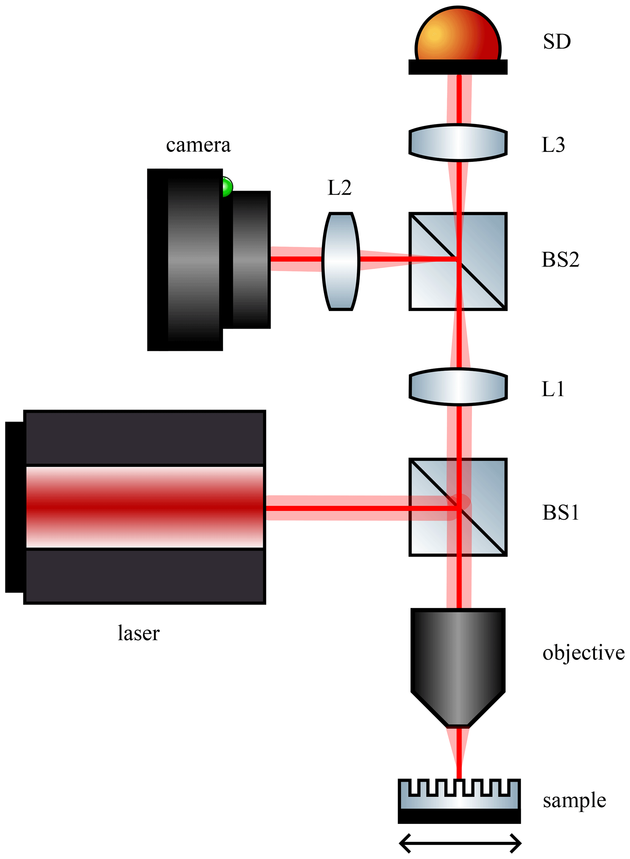
Figure 2Scheme of the coherent Fourier scatterometer setup. BS1 and BS2 are non-polarizing beam splitters, L1, L2 and L3 are lenses, and SD is the split detector.
3.3 White light interference microscopy
White light interferometry is an optical measurement method that exploits the interference of white light to measure the topology of structures in the micrometre-to-centimetre range. In combination with a microscope, WLIM can be implemented. Compared to a standard optical microscope, an interferometric objective lens and a precise positioning unit for the lens are required. In this way, the topography of the part of the sample that is just within the microscope's field of view can be imaged simultaneously without having to scan laterally (de Groot, 2015).
The device used here is NexView (Zygo Corporation, Middlefield, Connecticut, USA).
3.4 Atomic force microscopy
AFM is a very soft tactile measurement method which mechanically scans surfaces and measures the atomic forces and sample topography in the nanometre range. Such an instrument can be operated in different measuring modes, i.e. contact, non-contact, and tapping modes. In the measurements performed here, the tapping mode was used, providing less risk of tip damage on sharp edges of the defects than the contact mode. In this mode, the cantilever oscillates near its resonance frequency. Forces between the tip and the sample surface change the cantilever resonant frequency. Here, the most common regime was used, where a constant driving frequency is applied and a decay of the amplitude of the oscillations is used as a control signal when scanning over the sample surface, so that a control loop tries to keep the amplitude constant by adjusting the distance between the tip and the sample surface (Eaton and West, 2010).
For the measurements performed here, a Dimension Icon (Bruker, Billerica, Massachusetts, USA) has been used, with RTESPA-525 tapping-mode probes (resonant frequency of 525 kHz, nominal tip radius of 8 nm).
WLIM and AFM both map the topography of the sample. WLIM is significantly faster but also has a lower resolution than AFM due to the resolution limit.
4.1 Imaging ellipsometry
4.1.1 Ψ and Δ
The measurements of Ψ and Δ with the imaging ellipsometer have been performed on a polytype inclusion from Fig. 1d and on another polytype inclusion structure. Ellipsometric transfer quantities Ψ and Δ depend on the dielectric function of substrate and layer materials at the probing wavelength, layer thickness, and angle of incidence. By adjusting the corresponding measurement settings, it is possible to acquire the Ψ and Δ maps of defects with high lateral resolution and high contrast. Various defects can be clearly visualized in the transparent substrate and layer systems and classified according to their morphologies.
Figure 3a and b show overall-focused Ψ and Δ maps of type-C polytype inclusion in the homoepitaxial SiC layer on the SiC substrate from Fig. 1d. Defects of this type are detectable on both maps taken at an angle of incidence of 40° and a wavelength of 550 nm.
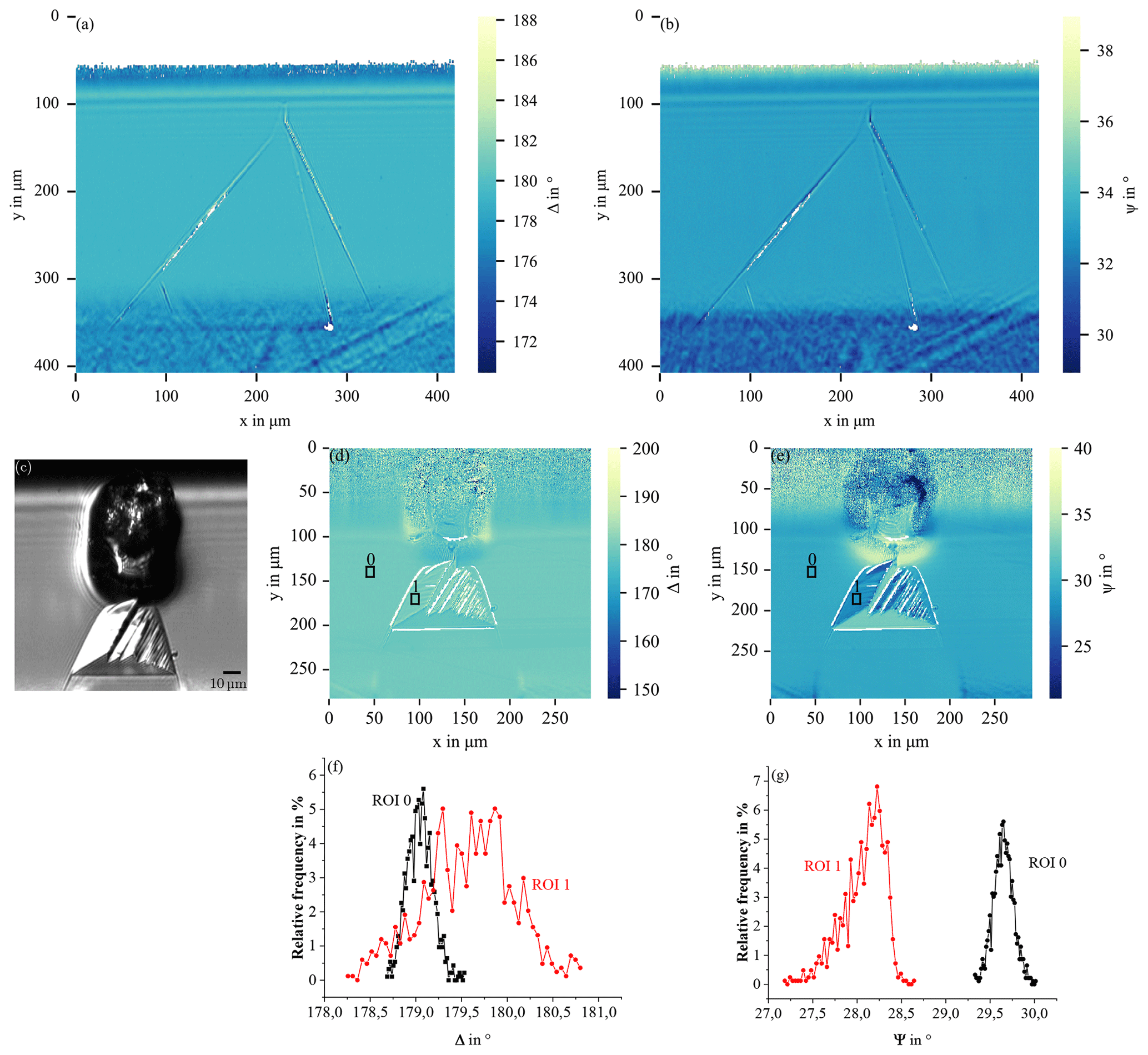
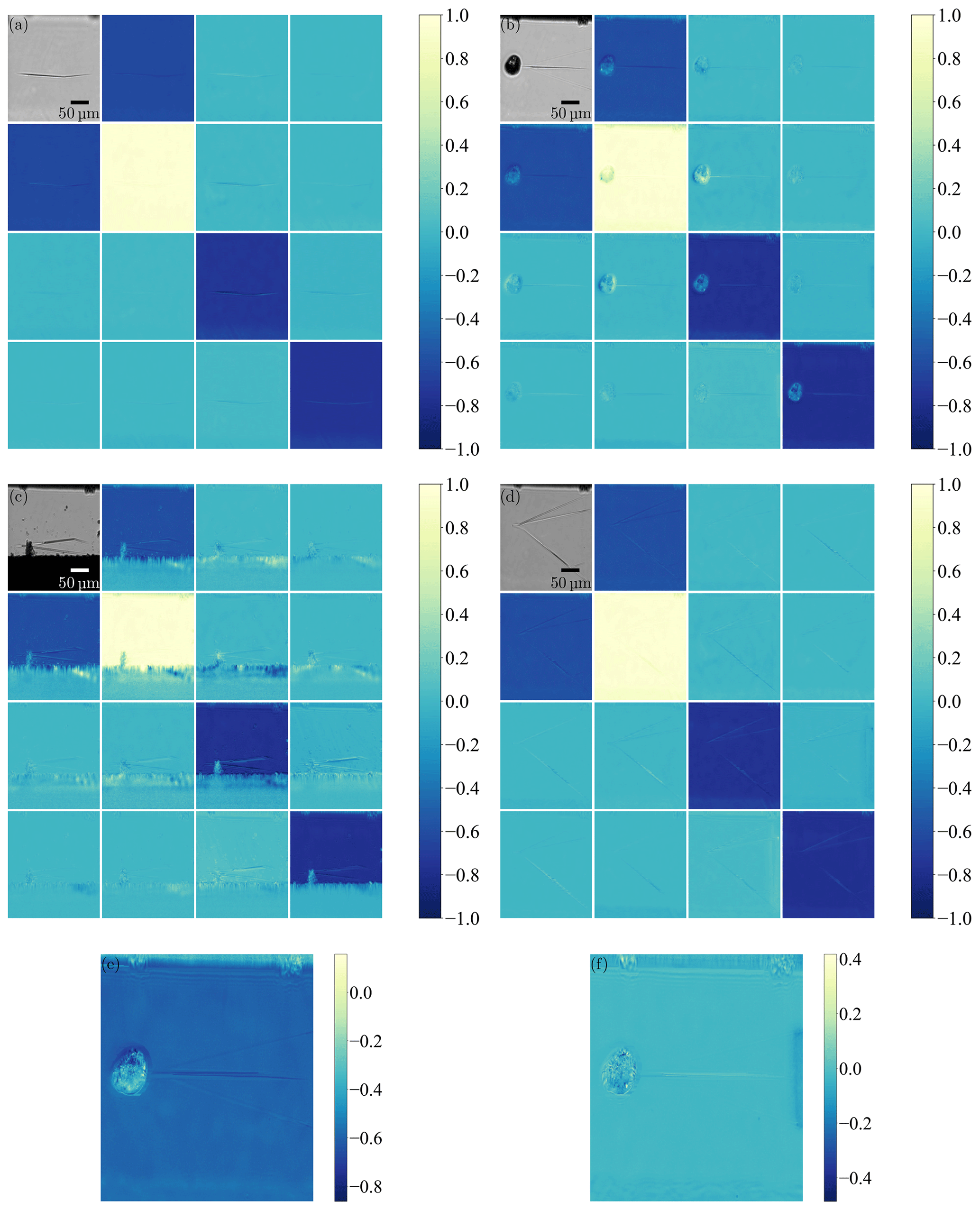
Figure 3Δ (a) and Ψ (b) maps of a polytype inclusion from Fig. 1d performed at 550 nm and at a 40° angle of incidence; overall-focused ellipsometric contrast microscopy image (c) of a polytype inclusion with particle; Δ (d) and Ψ (e) maps performed at a 550 nm wavelength and a 53° angle of incidence; histograms (f) and (g) of the corresponding regions of interest.
For a more detailed analysis, we can consider the type-A defect in Fig. 3c–e with a more complex structure consisting of two different areas. We show that the structural modification of the layer can be studied by means of a very informative statistical pixel-value analysis provided by an imaging ellipsometry setup. An overall-focused ellipsometric contrast microscopy image of the type-A defect can be seen in Fig. 3c. It was taken using a 10× objective at the angle of incidence AOI = 53°. The angles of the polarizer (P), the analyser (A), and the compensator (C) were P = 50°, A = 33°, and C = 45°, respectively. A focus scan is performed from the top to the bottom of the image and the overall-focused image is constructed from the stack of acquired line-focused images. Especially the step-like structure of the polytype inclusion can be seen very clearly. This is a polytype inclusion of type A. The focused scanned Ψ and Δ maps acquired with a 20× objective are shown in Fig. 3d and e. In the Ψ and Δ maps, the outlines of the polytype inclusion can be clearly detected. The particle is more clearly highlighted in the Ψ map than in the Δ map. The bright lines in the polytype inclusion part correspond to a low detected signal intensity (poor signal-to-noise ratio, SNR), which can be caused by multiple light scattering by inhomogeneous surface structures and resulting depolarization of reflected light. This effect may indicate non-uniformity of the epitaxial layer thickness (reduced thickness) in a triangular part of a defect and show that the structures visible in the ellipsometric contrast microscopy image in Fig. 3c represent the steep grooves. For both maps a region of interest (ROI) has been defined in the polytype inclusion part of the defect (ROI 1) and in the area outside the defect (ROI 0). Histograms for the respective ROIs can be seen in Fig. 3f and g. The measured Ψ and Δ pixel values in the selected ROIs are displayed on the horizontal axis. Ψ and Δ ranges are divided into a certain number of equal intervals and relative frequencies. That is, the number of pixel values within the interval relative to the entire number of pixels in the ROI are displayed on the vertical axis. Ψ and Δ distributions are found to be broader for ROI 1 within the defect than for ROI 0 outside the defect. Ψ values for ROI 1 are shifted towards lower values. Histogram analysis can indicate modified structures within the selected ROI 1 compared to the defect-free epitaxial layer surface in ROI 0 (Ermilova et al., 2023). Thus, a distinction can be drawn between the epitaxial layer and the defect. To clarify the topography of the defect, additional measurements were performed with WLIM.
4.1.2 Mueller matrix
As an extension to the Ψ and Δ measurements, IMME measurements have been performed on the structures shown in Fig. 1 at a wavelength of 500 nm and an angle of incidence of 50°. The results are shown in Fig. 4. Since all the elements are normalized to the m11 element, this element is always 1, and for this reason it is replaced here by a grey-scale image of the measured region. As can be seen in the results, the measurement system is sensitive to all four defects. On the main diagonal, the influence of reflection is clearly visible in all four cases. In the case of transmission this would be an identity matrix, and in the case of reflection the sign of the m33 and m44 elements changes. The defects have different amounts of influence on the polarization caused e.g. by different edge geometries or edge orientations. The carrot defects in Fig. 4a and c have little influence on the polarization. In Fig. 4b, when measuring the polytype inclusion with particle, the particle especially highlights very well, so it has a greater influence on the polarization than the surrounding surface. The line in the middle of the structure, which according to Chen et al. (2022) and Guo et al. (2017) represents an area that is not overgrown with 4H and that has a greater influence than the two outer lines of the polytype inclusion. For the polytype inclusion in Fig. 4d, something very similar can be observed: here, the lower line has a higher influence on the polarization than the other two. Further investigations should be carried out to verify whether a conclusion can be drawn from this as to which line is the one that has not been overgrown by 4H.
4.2 Coherent Fourier scatterometry
The defects from Fig. 1 have been measured with the CFS, and the measurement results are shown in Fig. 5. For the measurements a step size in the y direction of 0.2 µm has been applied. In Fig. 5b, impurities have been added around the particle, compared to the microscope image from Fig. 1b, which is probably due to transport of the sample to different labs.
4.3 White light interference microscopy
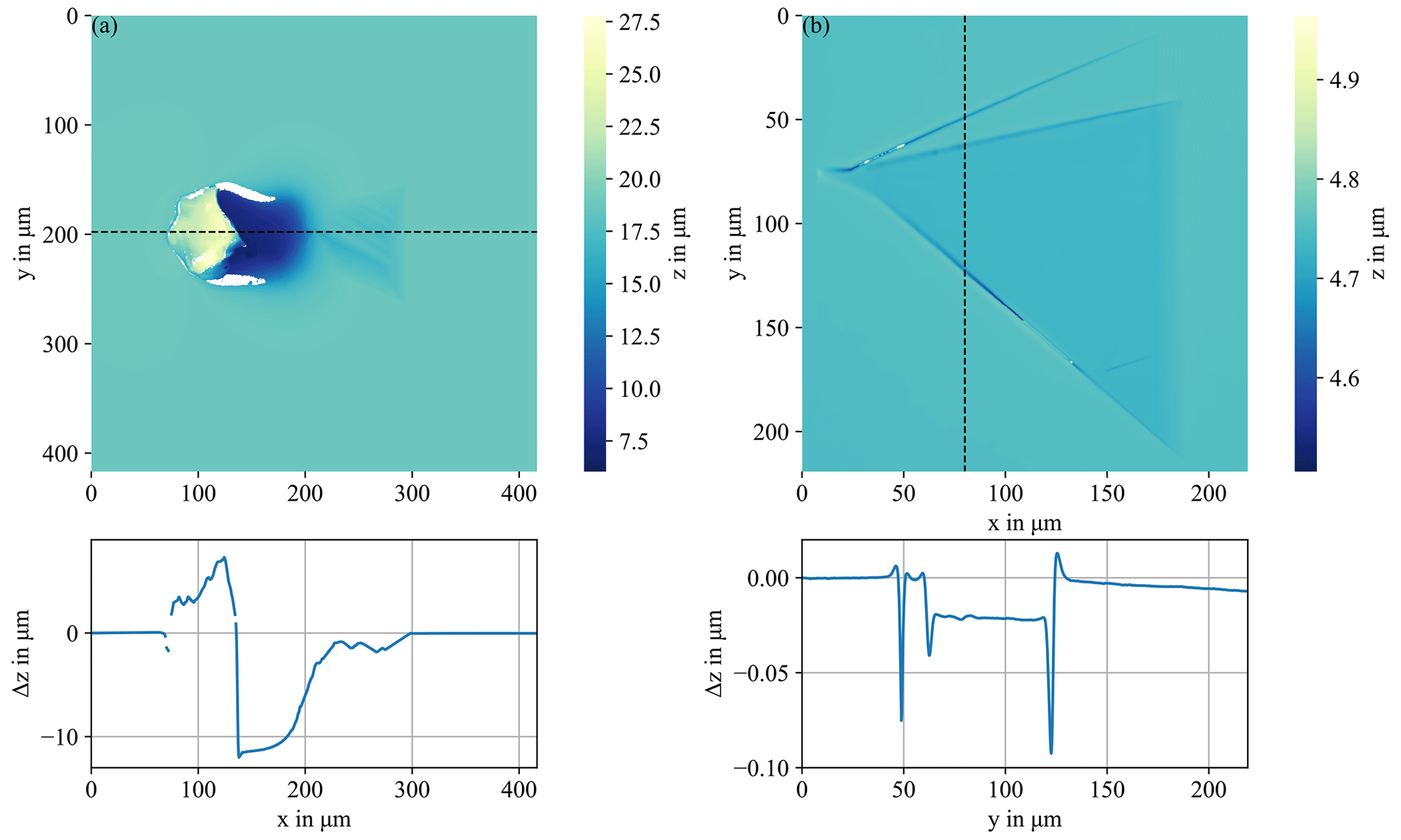
Figure 6 shows the two-dimensional WLIM images with associated height profiles of two polytype inclusions from Figs. 3c and 1d, respectively. The measurement in Fig. 6a was performed with a 20× Mirau objective and the measurement in Fig. 6b with a 20× objective and a 2× zoom. The horizontal axis of a profile corresponds to the distance along the dashed line on the sample surface. The vertical axis indicates the height at the corresponding point of a dashed line. The line profile in Fig. 6a shows that the particle of the polytype inclusion extends about 7 µm over the 4H-SiC epitaxial layer. After that, the profile line drops steeply over 11 µm towards the 4H-SiC substrate. The polytype inclusion part of the defect has V-shaped structures as shown in the height profile in Fig. 6a, which are located up to 2 µm inside the layer. These findings are consistent with suggestions that particles falling on the substrate before or during the epitaxy process can cause formation of polytype inclusions. In Fig. 6b, the plateau between the bottom and middle lines can be seen very clearly. This is about 20 nm deeper than the surrounding substrate. The outer lines in a defect visible in Fig. 6b correspond to a depth of more than 70 nm, showing that the defect structures are located within the epitaxial layer.
4.4 Atomic force microscopy
Using AFM, the defects shown in Fig. 1a, b and d have been measured together with additionally threading dislocations that seem to be TEDs with an explanation in Sect. 2. The results of these measurements are shown in Fig. 7. The carrot defect from Fig. 7a has a depth of about 70 nm. In the polytype inclusion from Fig. 7b, the 3C layer can be seen very well, which is completely overgrown by 4H-SiC steps. It is about 20 nm deeper than the surrounding surface. The line in the middle of the structure not overgrown with 4H is up to 120 nm deeper than the epitaxial layer. The TEDs in Fig. 7c have a depth of about 25 nm and a width of about 2 µm. These dislocations are found very often on the sample surface, which is consistent with the density distribution mentioned in Sect. 2. In the polytype inclusion in Fig. 7d, the plateau between the lower and middle lines can also be seen. This is about 20 nm deeper than the surrounding surface. The lines are up to 150 nm deeper than the epitaxial layer surface.
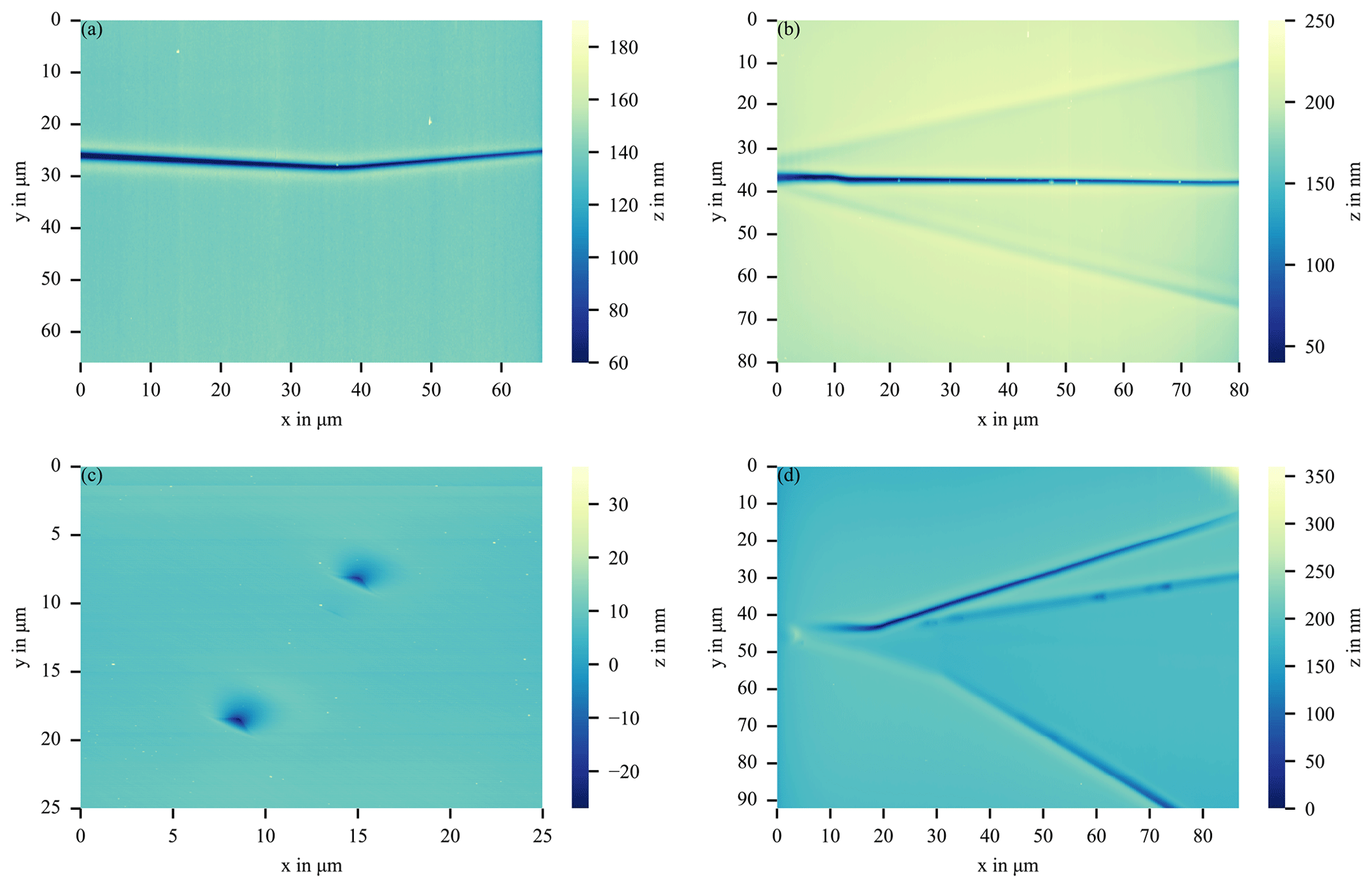
WLIM and AFM both represent the topography of the defects. Figures 6b and 7d show the results of the same defect. The topographies of the two measurements agree very well. The differences of the depths of the lines and the plateau are found identically in both measurement results. For such a structure, which has relatively large dimensions, the advantages of the WLIM measurement with a significantly shorter measurement time and a non-destructive measurement outweigh the disadvantages. The advantages of AFM apply to structures that are smaller than the resolution limit of WLIM, e.g. the TEDs in Fig. 7c.
All measurement methods used are sensitive to the defects studied here. Ellipsometry can detect the defects by analysing the images taken and searching for corresponding signals in the Mueller matrix or in Ψ and Δ. The polarization effects of the different defects can be studied. The analysis of the different areas of polytype inclusions is particularly interesting, as these are the most prominent in both the Mueller matrix images and the Ψ and Δ maps. Accordingly, imaging ellipsometry can be used for polytype inclusions, particles and carrots, but the focus should be on the polytype inclusions and particles. CFS detects the defects by scanning the focused laser beam over the sample. It can detect carrot defects, polytype inclusions and isolated nanoparticles and is therefore equally suitable for all of these three defect types. The advantage of both measurement methods is that they can analyse structures that are smaller than the wavelength used due to analysing the light–sample interaction via scattered light fields. AFM and WLIM measurement results are applicable for studying the topography of the defects. WLIM has the advantage of not having to scan laterally but can simultaneously image the topography of the part of the sample that is currently in the microscope's field of view. However, this means that the WLIM is restricted by the optical resolution limit. To avoid having to scan over the entire sample with AFM, the position information from ellipsometry, CFS or WLIM can be used to measure directly at the correct locations. Comparisons between the AFM and WLIM measurements at the same defects give identical results. The methods have different measurement speeds: for a measurement field of 100 µm × 100 µm IE needs several seconds to a minute for focused maps, CFS needs minutes, WLIM needs seconds, and AFM needs several minutes to tens of minutes. In general, the measurement time increases from WLIM over ellipsometry and CFS to AFM.
In comparison to other well-established methods for defect inspection, IE and CFS offer distinct advantages. They are non-destructive and measure quickly enough that they can also be used in-line. In addition, these methods can consider polarization properties, which have not been used much in the previously established methods.
A summary of the measurement methods is shown in Table 2.
To learn more about the exact structure of the defects, numerical simulations can be performed in the case of ellipsometry. This requires precise information about the materials used and their optical properties. Investigations are ongoing by combining the different measurement methods to get this required a priori information. With it, a model-based analysis of the IMME measurements on different defect types will be feasible, giving access to further structural and crystallographic defect details.
In conclusion, the choice of the most appropriate technique depends very much on the type of defect and what information is desired to make the right choice of measuring instrument. In general, a combination of different methods is required to get sufficient information about the type, size, and density of the present defects. Often it will be most efficient to start with a fast imaging method such as IMME to identify the locations of all the defects and then, depending on the defect type and further required information like defect depth, to combine this with one or more of the scanning metrology methods. If defects on the sample surface are to be found, ellipsometry, CFS, or even WLIM are suitable. If further information about the polarization properties, like edge orientations or edge geometries, is needed, then ellipsometry is suitable. If depth information of specific defects is needed, AFM or WLIM measurements can be performed.
Further investigations about suitable combinations of measurement methods in the different defect types are planned and will be published in a forthcoming paper.
Data underlying the results presented in this paper are available as raw data at https://doi.org/10.5281/zenodo.8382597 (Grundmann et al., 2023).
JG: performing imaging of Mueller matrix ellipsometry measurements, discussing results, writing the paper. BB: discussing results, writing the paper. EE: performing the Ψ and Δ imaging ellipsometry measurements, discussing results, writing the paper. MW: performing white light microscopy measurements. AH: discussing results. PK: performing atomic force microscopy measurements, discussing results, writing the paper. JR: performing coherent Fourier scatterometry measurements, discussing results. SFP: discussing results, writing the paper.
The contact author has declared that none of the authors has any competing interests.
Publisher’s note: Copernicus Publications remains neutral with regard to jurisdictional claims made in the text, published maps, institutional affiliations, or any other geographical representation in this paper. While Copernicus Publications makes every effort to include appropriate place names, the final responsibility lies with the authors.
This article is part of the special issue “Sensors and Measurement Science International SMSI 2023”. It is a result of the 2023 Sensor and Measurement Science International (SMSI) conference, Nuremberg, Germany, 8–11 May 2023.
This project (20IND09 PowerElec) PowerElec has received funding from the EMPIR programme co-financed by the Participating States and from the European Union's Horizon 2020 research and innovation programme.
The authors thank AIXTRON for providing the samples.
This research has been supported by the European Metrology Programme for Innovation and Research (grant no. 20IND09 PowerElec).
This paper was edited by Michael Kraft and reviewed by three anonymous referees.
Alves, L. F. S., Gomes, R. C. M., Lefranc, P., de A. Pegado, R., Jeannin, P.-O., Luciano, B. A., and Rocha, F. V.: SiC power devices in power electronics: An overview, in: 2017 Brazilian Power Electronics Conference (COBEP), Juiz de Fora, Brazil, 19–22 November 2017, IEEE, 1–8, https://doi.org/10.1109/COBEP.2017.8257396, 2017. a
Aspnes, D. E.: The Accurate Determination of Optical Properties by Ellipsometry, in: Handbook of Optical Constants of Solids, edited by: Palik, E. D., Academic Press, 89–112, ISBN: 0-12-544420-6, 1985. a
Azzam, R. M. A. and Bashara, N. M.: Ellipsometry and Polarized Light, North-Holland, New York, ISBN 0720406943, 1977. a
Benamara, M., Zhang, X., Skowronski, M., Ruterana, P., Nouet, G., Sumakeris, J. J., Paisley, M. J., and O'Loughlin, M. J.: Structure of the carrot defect in 4H-SiC epitaxial layers, Appl. Phys. Lett., 86, 021905-1–021905–3, https://doi.org/10.1063/1.1849416, 2005. a, b
Chen, P.-C., Miao, W.-C., Ahmed, T., Pan, Y.-Y., Lin, C.-L., Chen, S.-C., Kuo, H.-C., Tsui, B.-Y., and Lien, D.-H.: Defect Inspection Techniques in SiC, Nanoscale Res. Lett., 17, 30, https://doi.org/10.1186/s11671-022-03672-w, 2022. a, b, c, d
Chipman, R. A.: Polarimetry, in: Handbook of Optics, edited by: Bass, M., van Stryland, E. W., Williams, D. R., and Wolfe, W. L., McGraw-Hill, 2, 22.1–22.37, ISBN: 0-07-047974-7, 1994. a
de Groot, P.: Principles of interference microscopy for the measurement of surface topography, Adv. Opt. Photonics, 7, 1–65, https://doi.org/10.1364/AOP.7.000001, 2015. a
Eaton, P. and West, P.: Atomic Force Microscopy, Oxford University Press, ISBN: 978-0-19-957045-4, 2010. a
Ermilova, E., Weise, M., and Hertwig, A.: Application of imaging ellipsometry and white light interference microscopy for detection of defects in epitaxially grown 4H-SiC layers, J. Eur. Opt. Soc.-Rapid, 19, 23, https://doi.org/10.1051/jeos/2023018, 2023. a
Funke, S., Miller, B., Parzinger, E., Thiesen, P., Holleitner, A. W., and Wurstbauer, U.: Imaging spectroscopic ellipsometry of MoS2, J. Phys.-Condens. Mat., 28, 385301, https://doi.org/10.1088/0953-8984/28/38/385301, 2016. a
Gawhary, O. E., Kumar, N., Pereira, S. F., Coene, W. M. J., and Urbach, H. P.: Performance analysis of coherent optical scatterometry, Appl. Phys. B-Laser. O., 105, 775–781, https://doi.org/10.1007/s00340-011-4794-7, 2011. a
Goldstein, D.: Mueller Matrix Polarimetry, in: Polarized Light, edited by: Thompson, B. J., Marcel Dekker, Inc., 2nd edn., ISBN: 0-8247-4053-X, 2003. a, b
Grundmann, J., Bodermann, B., Ermilova, E., Weise, M., Hertwig, A., Klapetek, P., Rafighdoost, J., and Pereira, S. F.: Optical and Tactile Measurements on SiC Sample Defects - Dataset, Version v1, Zenodo [data set], https://doi.org/10.5281/zenodo.8382597, 2023. a
Guo, J., Yang, Y., Raghothamachar, B., Kim, T., Dudley, M., and Kim, J.: Understanding the microstructures of triangular defects in 4H-SiC homoepitaxial, J. Cryst. Growth, 480, 119–125, https://doi.org/10.1016/j.jcrysgro.2017.10.015, 2017. a, b, c, d
Hallin, C., Konstantinov, A. O., Pecz, B., Kordina, O., and Janzen, E.: The origin of 3C polytype inclusions in epitaxial layers of silicon carbide grown by chemical vapour deposition, Diam. Relat. Mater., 6, 1297–1300, 1997. a
Hassan, J., Henry, A., McNally, P. J., and Bergman, J. P.: Characterization of the carrot defect in 4H-SiC epitaxial layers, J. Cryst. Growth, 312, 1828–1837, https://doi.org/10.1016/j.jcrysgro.2010.02.037, 2010. a
Hecht, E.: Polarization, in: Optics, edited by: Black, A., Addison-Wesley, 4th edn., 325–384, ISBN: 0-321-18878-0, 2002. a
Konstantinov, A. O., Hallin, C., Pecz, B., Kordina, O., and Janzen, E.: The mechanism for cubic SiC formation on off-oriented substrates, J. Cryst. Growth, 178, 495–504, 1997. a
Li, H., Cui, C., Lu, J., Hu, Z., Lin, W., Bian, S., and Xu, X.: Mueller matrix ellipsometric characterization of nanoscale subsurface damage of 4H-SiC wafers: from grinding to CMP, Front. Phys., 9, 820637, https://doi.org/10.3389/fphy.2021.820637, 2022a. a
Li, J., Yang, G., Liu, X., Luo, H., Xu, L., Zhang, Y., Cui, C., Pi, X., Yang, D., and Wang, R.: Dislocations in 4H silicon carbide, J. Phys. D Appl. Phys., 55, 463001, https://doi.org/10.1088/1361-6463/ac8a58, 2022b. a
Losurdo, M. and Hingerl, K. (Eds.): Ellipsometry at the Nanoscale, Springer, https://doi.org/10.1007/978-3-642-33956-1, 2013. a
Rafighdoost, J., Kolenov, D., and Pereira, S. F.: Coherent Fourier Scatterometry for Detection of Killer Defects on Silicon Carbide Samples, IEEE T. Semiconduct. M., 37, 124–128, https://doi.org/10.1109/TSM.2023.3337720, 2023. a
Raymond, C. J.: Scatterometry for Semiconductor Metrology, in: Handbook of Silicon Semiconductor Metrology, edited by Diebold, A. C., Marcel Dekker, Inc., ISBN: 0-8247-0506-8, 2001. a
Roy, S., Bouwens, M., Wei, L., Pereira, S. F., Urbach, H. P., and van der Walle, P.: High speed low power optical detection of sub-wavelength scatterer, Rev. Sci. Instrum., 86, 123111, https://doi.org/10.1063/1.4938183, 2015. a, b
Si, W., Dudley, M., Kong, H.-S., Sumakeris, J., and Carter, C.: Investigations of 3C-SiC Inclusions in 4H-SiC Epilayers on 4H-SiC Single Crystal Substrates, J. Electron. Mater., 26, 151–159, https://doi.org/10.1007/s11664-997-0142-4, 1997. a
Treu, M., Vecino, E., Pippan, M., Häberlen, O., Curatola, G., Deboy, G., Kutschak, M., and Kirchner, U.: The role of silicon, silicon carbide and gallium nitride in power electronics, in: 2012 International Electron Devices Meeting, San Francisco, CA, USA, 10–13 December 2012, IEEE, 7.1.1–7.1.4, https://doi.org/10.1109/IEDM.2012.6478995, 2012. a
Wilson, L., Ishiuchi, H., Gargini, P., Allan, A., Balestra, F., Hayashi, Y., and Kenny, L.: Executive Summary, in: 2021 IEEE International Roadmap for Devices and Systems Outbriefs, Santa Clara, CA, USA, 30 November 2021, IEEE, 1–64, https://doi.org/10.1109/IRDS54852.2021.00007, 2021. a, b
Yu, J., Yang, X., Peng, Y., Hu, X., Wang, X., Chen, X., and Xu, X.: Revelation of the dislocations in the C-face of 4H-SiC substrates using a microwave plasma etching treatment, CrystEngComm, 23, 353–359, https://doi.org/10.1039/d0ce01489c, 2021. a
Zhao, L.: Surface defects in 4H-SiC homoepitaxial layers, Nanotechnol. Precis. Eng., 3, 229–234, https://doi.org/10.1016/j.npe.2020.12.001, 2020. a