the Creative Commons Attribution 4.0 License.
the Creative Commons Attribution 4.0 License.
 | 08 Jul 2024
Concept, simulation, and fabrication of inverted grating structures for surface plasmon resonance sensors
Pongsak Sarapukdee
Dirk Schulz
Stefan Palzer
Surface plasmon resonance (SPR) sensors offer the possibility of label-free analysis of biosamples. The long-term stability of standard approaches is limited due to degradation of the grating upon contact with the analyte, and strategies to improve the performance in this regard include the use of so-called inverted configurations. By exciting surface plasmons from the back side of the grating, this design overcomes limitations of traditional grating-based SPR sensors caused by direct contact with the analyte medium and offers new design possibilities for implementing microfluidic analytical systems. Here a simulation for optimizing design parameters and a corresponding microfabrication technology to create the inverted grating are presented. An experimental evaluation of surface plasmon excitation and sensitivity enhancement demonstrates the feasibility of the approach. While the observed coupling effect of inverted grating structures is not as strong as the conventional configuration, it offers benefits like preventing surface oxidation, enabling repeated usage and new concepts for biosample processing.
- Article
(4610 KB) - Full-text XML
- BibTeX
- EndNote


Surface plasmon resonance (SPR) sensors have emerged as powerful tools for label-free detection and real-time monitoring of biomolecular interactions (Samuel and Rao, 2022). Unlike conventional methods that require labelling of molecules with fluorescent or radioactive tags, SPR sensors directly detect changes in the refractive index near the sensor surface, thus enabling sensitive and quantitative analysis of biomolecular interactions. One common design approach for SPR sensors involves the use of a grating structure to couple incident light with surface plasmons, which are collective oscillations of electrons at the metal–dielectric interface. The grating structure enhances the sensitivity of the sensor by increasing the interaction area between the surface plasmons and the analyte molecules (Arora et al., 2018). A grating SPR sensor is well-suited for integration with small devices due to its compact size and compatibility for microintegration, which can further enhance their utility and versatility in various applications (Mahmud et al., 2023).
However, traditional grating-based SPR sensors have certain limitations that affect their performance. One significant issue is the direct contact of the analyte medium with the grating surface (Kotlarek et al., 2019; Wood et al., 2019; Sarapukdee et al., 2023; Rossi et al., 2018). Past research highlights various difficulties in developing grating-based SPR sensors when the light wave is incident from the front and travels through the sensing fluid. Firstly, the presence of the sensing fluid might alter the intensity, polarization, and phase of the reflected light, adding noise to the detection process. Secondly, turbid or bubbling testing fluids can scatter reflected light, confounding measuring results. Thirdly, direct contact of incident light with biological samples under test may cause damage or induce changes in the samples, resulting in unreliable measurement results. These findings emphasize the need to evaluate alternative sensor configurations to circumvent potential effects of direct contact with the analyte medium. In the past, both simulations and experimental studies have examined SPR excitation through backside illumination of the grating (Pi et al., 2016; Lindquist et al., 2012; Saito et al., 2019a, b; Kuo et al., 2019; Yoon et al., 2006) with the aim of enabling more robust sensing devices. Basically, the inverted configuration can mitigate the detrimental effects caused by direct contact with the analyte medium and enable new designs of the sample cell and sample handling. By employing a non-pass-through or backside-incident approach, the inverted grating design minimizes noise from sensing fluid interactions, offers greater compatibility with diverse sample types, and reduces the risk of sample damage. The inverted grating configuration offers the potential to enhance measurement accuracy and reliability, making it a promising technique in grating-based surface plasmon resonance sensing technology.
The field of plasmonic sensors based on flat finished grating structures and back-illumination has seen significant research over the past decade, with numerous studies exploring various designs and applications. To this end, several groups have investigated sophisticated designs using various material systems and grating designs. Iqbal et al. (2022) showed the potential of buried gold (Au) grating to enhance the sensitivity. Using a nanoslit design making use of two dielectric and two metallic layers, Elshorbagy et al. (2017) demonstrated an indirect SPR excitation approach for the refractive index range between n = 1.33 and 1.36 using NIR laser sources. A similar refractive index range was investigated by Kong et al. (2020) using a combination of a prism and a grating structure embedded in thin silver (Ag) layers to excite SPR. In order to shield the Ag from the analyte, a graphene layer was deposited. An arsenic selenide (As2Se3)-based approach combined with a gold (Au) layer and laser excitation in the NIR spectral range was investigated by Joseph et al. (2020) to show a detection range between n = 1.33 and 1.345.
However, in order to lower production costs and facilitate fabrication of large numbers of SPR sensors, a reduction in system complexity and the possibility of using excitation sources in the visible spectral range are possible building blocks. For SPR systems operating in the visible spectrum, silver is a worthwhile material to study, since it is known as a low-loss, high-performance material. To advance knowledge in this regard, the possibility of using comparatively simple, silver-based inverted grating structures with SPR excitation in the visible range is investigated here. Consequently, this work focuses on utilizing silver as the plasmonic material since it offers high sensitivity and cost-effectiveness as compared to other materials. Silver allows for enhanced sensing capabilities while remaining economically viable. The fabrication process involves direct deposition onto glass substrates, eliminating the need for expensive substrates and making the device more accessible and affordable. The study introduces novel insights and considerations into the design and fabrication of plasmonic sensors, offering an added perspective to the challenges and opportunities in this field. The experimental results of the systems are used to provide real-world confirmation of the proposed simulation environment.
In this work, an inverted grating structure has been simulated, designed, and fabricated using microsystems technology. The performance in terms of surface plasmon excitation and sensitivity enhancement has been evaluated for a refractive index range of n = 1.0–1.6. The grating coupler is simulated in order to optimize its design parameters, fabricate the inverted grating structure on glass substrates, and experimentally measure the surface plasmon response using a dedicated optical setup. By exploring the potential of the inverted grating structures, advances in the field of fabricating inverted grating SPR sensors may be achieved, thus contributing to overcoming the limitations of traditional grating-coupler designs using materials and technologies that enable reproducible fabrication using microsystems technology. The traditional SPR sensor concept and the inverted configuration are depicted in Fig. 1 to highlight the differences in the respective concepts and demonstrate the potential for novel system designs based on inverted grating couplers.

Figure 1(a) The schematic design illustrates the utilization of an inverted grating with polydimethylsiloxane (PDMS) microchannels. The microtube obstructs the illumination light on the front side, while the back side (b) offers advantages for assembly.
This work describes the complete development cycle, including fabrication, characterization, and simulation, to enable an efficient and iterative optimization of grating structures. The computer modelling steps used in this study are illustrated in Fig. 2 and aim at providing a simulation environment capable of providing accurate predictions of the real-world behaviour of the system.

Figure 2The simulation environment has been built to incorporate experimental results in order to obtain more accurate models, which describe the real-world behaviour of the inverted structures.
Therefore, a computer model has been built using preliminary experimental data including material parameters and grating designs. Due to its potential for highly sensitive SPR sensor couplers, silver has been chosen as the grating material in this study. For technological reasons, an adhesion layer of nickel is needed, and the material parameters of both have been considered for the simulation model. The outcomes of laboratory experiments have then been compared to the results of a computer model. Finally, parameters have been adjusted in order to obtain results in line with the experimental results. The process is iterative and may be repeated with new experimental results to fine-tune the computer model further. In this way, a computer model for plasmonic grating couplers using an inverted configuration for biosensor applications has been built. This model has also been used to predict the results of upcoming experiments. The model has been studied in order to assess its accuracy in predicting the behaviour of novel structures.
The simulation is based on MATLAB using the finite-difference time domain (FDTD) method (Archambeault et al., 2001) along with the Drude model method (Levi, 2016) to model the behaviour of the grating structure. Additional techniques integrated into the simulation environment include perfectly matched layer (PML) (Bérenger, 2007), periodic boundary condition (PBC) (Li and Sarris, 2009), and the total-field/scattered-field method (TF/SF) (Zhang et al., 2020), which are crucial for accurately simulating the reflectivity of the grating structure. An inverted grating has been designed on a glass substrate, necessitating verification of the manufacturing parameters. Notably, the simulation model has been verified with a conventional front-side grating, as shown in Fig. 3, where a light wave of 632.8 nm wavelength is utilized by employing polarized light with a power of 1 mW. The values for the material properties have been implemented using a dielectric constant of −11.4 at an excitation wavelength of 632.8 nm for the nickel layer (εNi) and a permittivity of −19 for silver (εm). Additionally, the model has furthermore used permittivity values of 2.1 for glass (εd) and 1 for air (εair) to accurately represent the optical properties of the materials involved. These values were chosen based on the validation of the model against experimental results from previous studies (Sarapukdee et al., 2023), where the provided values for the dielectric constants yielded accurate predictions and consistent outcomes. Therefore, the dielectric constant values used in this model reflect the values that were most appropriate and effective for achieving agreement with experimental observations.
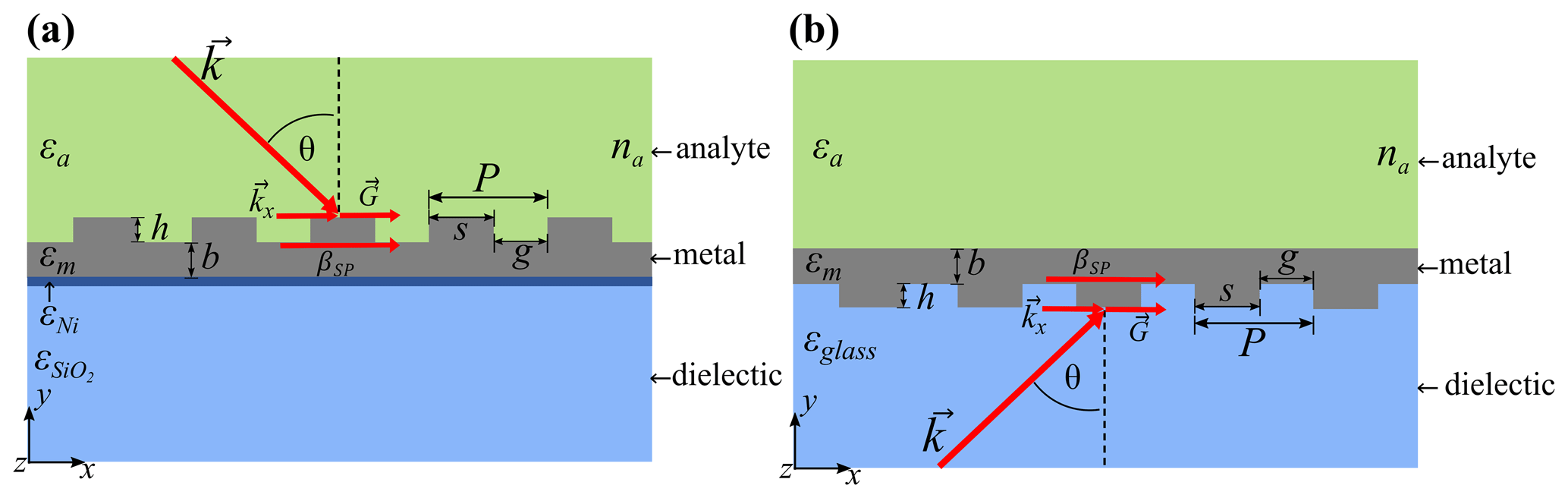
Figure 3The diagram depicts grating structures. (a) Front-side grating: a periodic groove structure in an analyte substance (εa). The incident wave (k) interacts with the grating at an angle θ, resulting in a diffracted wave that propagates in the direction of the surface plasmon wave (βSP). (b) The inverted grating structure consists of a metallic layer (εm) on top of a glass substrate (εglass). The incident wave initially interacts with the glass substrate and then with the grating structure, allowing analyte material contact to occur above the metal layer.
After validating the model, the structure has been redesigned from the conventional front-side grating to an inverted grating, as depicted in Fig. 3. The structural parameter range that has been considered consisted of a symmetric, rectangular grating structure with a periodicity P of 500–800 nm, i.e. a grating groove size s of 250–400 nm, a gap between the grating groove g of 250–400 nm, a nickel layer of 5 nm, and a silver base thickness b of 40–50 nm, and preliminary simulation results revealed that, when the grating groove height surpassed that of the silver base, a peak vanishes. Consequently, the setup focused exclusively on structures where the height remains below the silver base layer. Specifically, for a silver base thickness b = 40 nm, the heights considered were 20, 30, and 40 nm. However, for b = 50 nm, the heights tested ranged from 20 to 50 nm. Plasmon excitation angles ranging from 10 to 70° were carefully investigated in order to determine the best structure. These evaluations were carried out using incident angles directed at the grating structure's surface, with the goal of obtaining a thorough understanding of its characteristics.
Exemplary simulation results, as illustrated in Fig. 4, reveal the relative reflection profile and plasmon excitation angles for inverted configurations. These simulation results yield primary candidates for the fabrication process in the upcoming experiments and highlight the importance of precise nanostructuring that is necessary to obtain sensitive and reproducible devices. Figure 4b showcases the coupling efficiency (CE) − calculated as (100 − relative reflection) FWHM − revealing two configurations that yielded optimal results: silver base thickness b = 50 nm, groove height h = 20 nm, b = 40 nm, and h = 20 nm. These configurations demonstrated excellent coupling efficiency, setting the stage for taking design decisions. It is important to note that Fig. 4 only shows the structure with a periodicity of 500 nm, as it has the maximum coupling efficiency among periodicities of 500–800 nm.
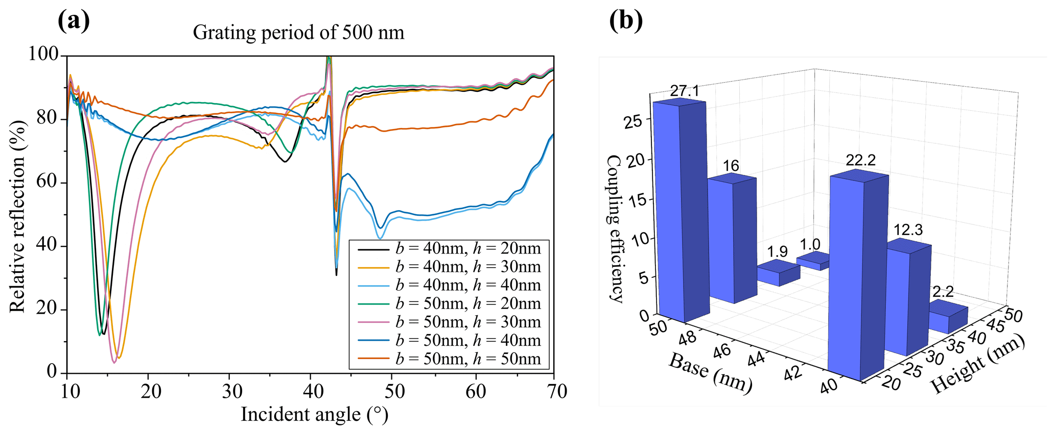
Figure 4(a) Sample simulation results of the inverted grating model for a grating periodicity Λ = 500 nm, varying silver base thickness of 40–50 nm, and grating groove height of 20–40 nm. (b) The highest coupling efficiency is 27.1, achieved from the silver base thickness of 50 nm and grating groove height of 20 nm.
Balancing performance with the complexity of fabrication is often a key consideration in experimental setups. After careful evaluation, it became evident that, while both configurations provided excellent coupling efficiency, the combination of b = 50 nm and h = 30 nm emerged as the ideal choice. This configuration strikes a balance between performance and ease of fabrication, making it the preferred choice for the inverted grating design.
To determine the optimal structure, plasmon excitation angles ranging from 10 to 70° have been evaluated since characterization via the home-built measurement station offers this range. It is important to note that the incident angles at the grating structure are calculated by accounting for the refractive index of the glass medium, employing Snell's law (Pedrotti et al., 2019) to accurately determine the angles of incidence.
In order to estimate the sensitivity of the structure, varying refractive indices have been introduced into the model, and the results are shown in Fig. 5. The measurement ranges up to refractive indices of 1.6 indicate the possibility of biosample analysis with a high dynamic range. While the first-order excitations provide a more pronounced dip, the peak width is also much broader. From the signal profile of the grating measurement results, please refer to the explanation of the grating diffraction order from Dai et al. (2018). The +1- and −2-order SPR dips occur at angles of 15.8 and 34.8°, respectively.

Figure 5(a) The influence of the sample's refractive index on the plasmon excitation demonstrates the sensitivity of inverted structures in first- (m = + 1), second- (m = −2), and third-order (m = +3) couplings. (b) Graph illustrating the relationship between the plasmon excitation angle and refractive index units: the first-order and second-order angle shows minimal change with a varying refractive index, while the third orders (S = 31° RIU−1, FOM = 47 RIU−1) exhibit shifts.
Remarkably, despite variations in the refractive index, these dips remained relatively stable. A possible explanation is that SPR is excited at the silver–substrate interface. This excitation angle appears to be unaffected by changes in the analyte layer. In contrast, the +3-order SPR dip exhibited a dynamic response closely tied to changes in the refractive index. It displayed a sensitivity of 31° RIU−1, corresponding to a figure of merit (FOM) of 47 RIU−1. The shift in the excitation angle is directly correlated with changes in the surrounding medium, making it a promising tool for monitoring alterations in analyte properties.
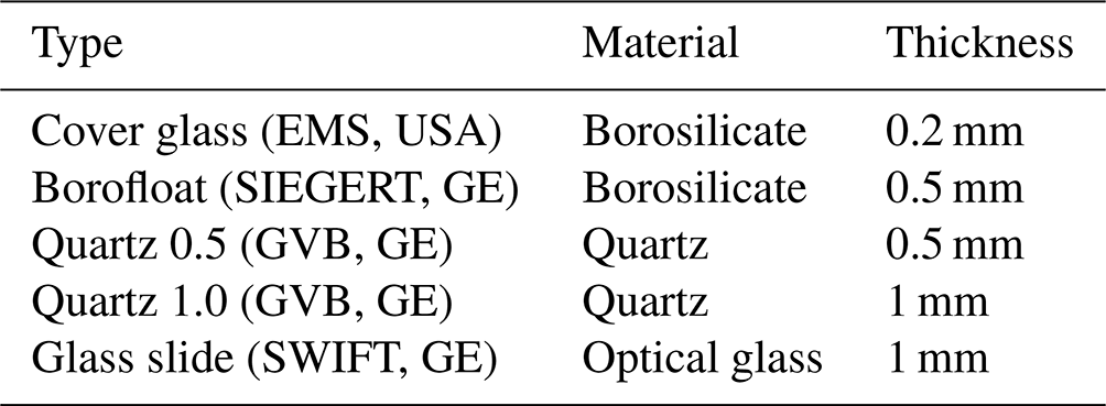
In the first step of the technology flow development, the most suitable glass to form the base of the inverted grating structure was determined experimentally. Different glasses were considered based on factors like commercial availability, cost-effectiveness, heat resistance, and corrosion resistance. Since the fabrication process involves multiple steps, it was crucial to choose a substrate that is compatible with the construction process. Table 1 shows various substrates that have been investigated with different materials and thicknesses.
Table 1Overview of the different glass types and thickness details.
Commercially available glass typically comes in a size of (2 × 2) cm2; larger glasses were cut to a similar size, except for quartz glass, which was available in a (1 × 1) cm2 size. Prior to testing, the samples were cleaned with isopropyl alcohol (IPA) and allowed to dry. The experiment involved sputtering nickel onto the surface to form a seeding layer, followed by the deposition of a smooth silver layer at a rate of 0.15 nm s−1. A 100 nm thick silver layer was then thermally evaporated over the nickel seed layer. The samples were tested to observe how light transmits through the substrate without the grating structure affecting the behaviour, i.e. merely determining the reflectivity at different illumination angles. Figure 6 illustrates the glass testing configuration. Therefore, the reflected signal should remain consistent, without recognizable dip angles, and have a high light intensity, indicating that the glass does not absorb light effectively.
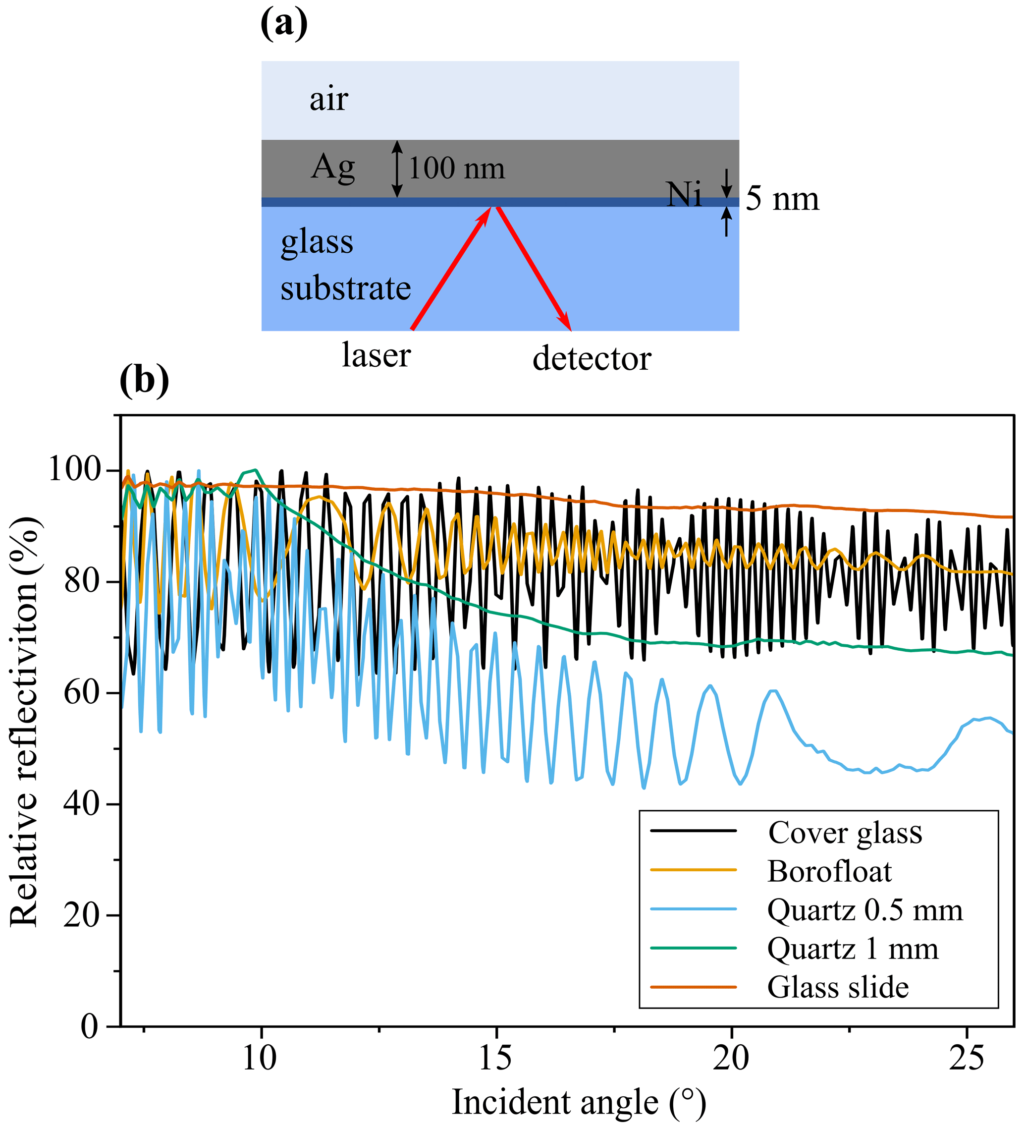
Figure 6(a) Measuring various types and thicknesses of glass substrates with a 100 nm silver layer on the back side but without excitation of surface plasmons. (b) The relative reflection results indicate the effect of interval reflection, leading to an interference effect when tilting the excitation angle. A clear signal can only be appreciated from the glass slide (red line) and quartz 1 mm (green line).
The fabrication of the inverted grating consequently continued on a clear glass substrate and required a new measurement method to overcome the challenge of analysing gratings without blocking light passing through the transparent glass. The main microfabrication steps are shown in Fig. 7 and mainly rely on using poly(methyl methacrylate) (PMMA) as an e-beam sensitive photoresist in combination with reactive-ion etching for structuring.
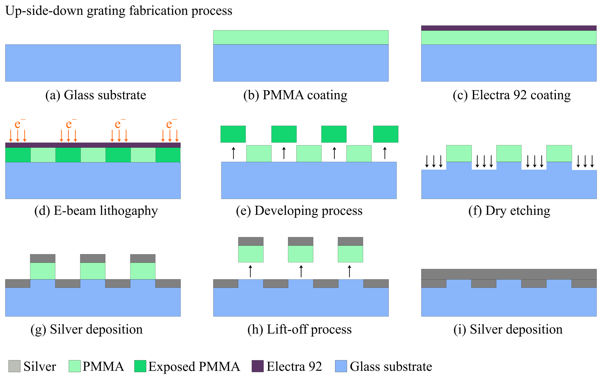
Figure 7Fabrication process for inverted grating: (a) initially, a glass substrate measuring (2 × 2) cm2 was divided into equal squares. (b–c) Following that, the substrate was coated with e-beam resists and a conductive layer. (d) The grating structure was then meticulously patterned using the e-beam lithography technique. (e) Subsequently, the exposed e-beam resist and the conductive layer were removed through a chemical development process. (f) Reactive ion etching was conducted to the same depth as the desired groove height h of the grating structure. (g) The first layer of silver was deposited onto the substrate via thermal evaporation. (h) A lift-off process was then employed to eliminate the resist, followed by (i) the deposition of the second layer of silver, forming the silver base thickness b for the grating structure.
To achieve inverted grating structures, a photoresist layer of 250 nm PMMA is initially applied to the glass substrate. However, due to the high insulating properties of glass, scanning electron microscopy (SEM) image reproduction at the nanoscale was of poor quality. To improve conductivity, Electra 92 (AR-PC 5090.02, Allresist GmbH) was used. This allowed for the commencement of e-beam construction and development processes. The next step involved etching the inverted grating structure into the glass substrate using reactive-ion etching (RIE, Oxford PlasmaLab 80Plus, Oxford Instruments) to match the depth of the grating groove height h. Subsequently, the first silver layer was deposited at the same height to create the silver grating within the glass substrate. The lift-off process was then utilized to remove the silver layer above the photoresist. Afterwards, the second silver layer was deposited to establish the base of the grating structure. Additional layers of corrosion protection may be applied as needed to enhance the overall durability and performance of the grating. By following this process, the fabrication of the inverted grating on the clear glass substrate can be accomplished.
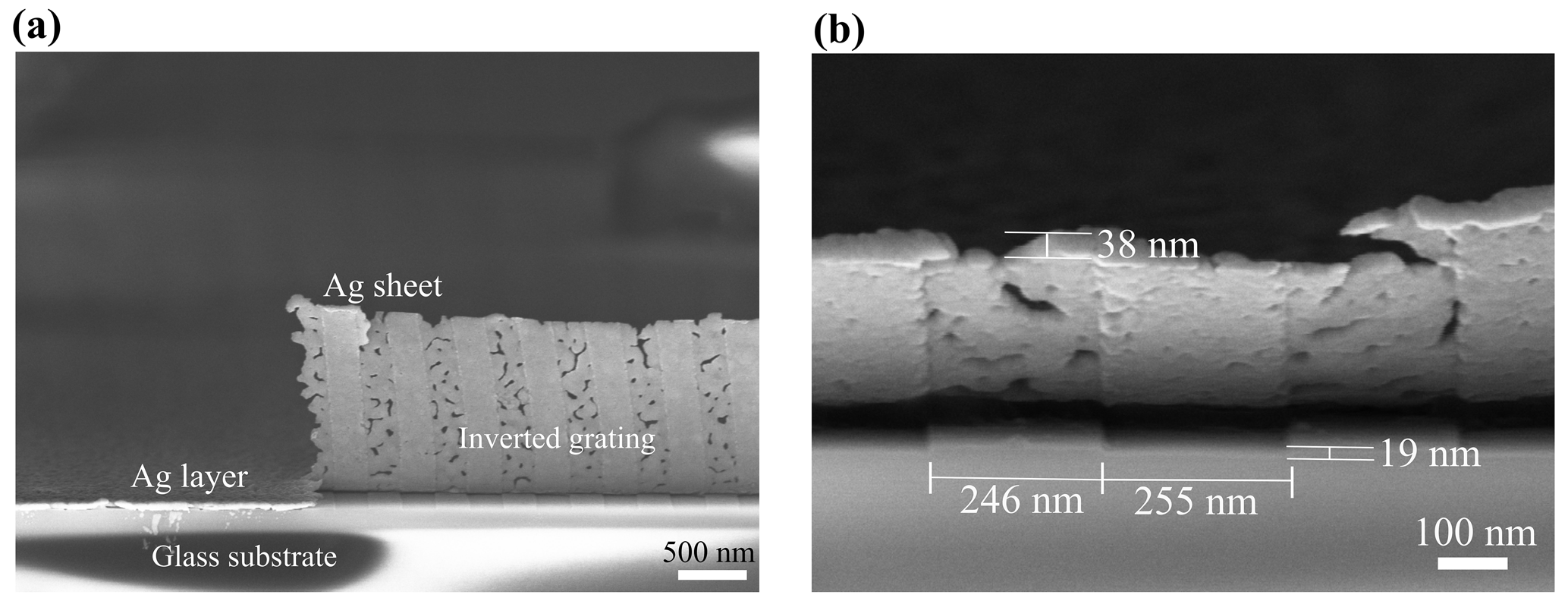
Figure 8The SEM cross-sectional image of the inverted grating structure reveals a peeled sheet of silver metal, indicating porosity due to the absence of an adhesive layer. The substrate also displays an etching depth matching the grating groove height h of (20 ± 2) nm, a grating groove size of (250 ± 5) nm, and a base thickness of (40 ± 3) nm.
Following the results of the simulation, the structural parameters of the grating to be fabricated were chosen. The morphology of the produced structures has been assessed using SEM analysis, and exemplary results are shown in Fig. 8. To assess the performance of the grating structures, surface plasmons were excited using a custom measurement setup as shown in Fig. 9. A 632.8 nm helium–neon gas laser (05-LHP-151, Melles Griot) was employed, and its polarization was adjusted with an integrated polarizer to produce a linearly polarized beam for ideal coupling. The beam intensity was set to 1 mW using a neutral density filter (ND filter), and a plano-convex lens with a focal length of f = 300 mm was used to collimate the near-ideal Gaussian beam with a 3 mm diameter and block higher-order Gaussian-mode contributions.
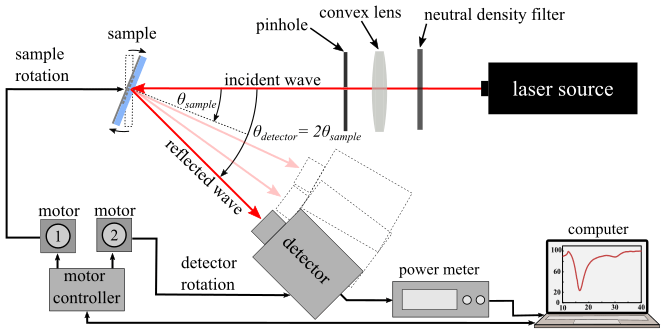
Figure 9Experimental setup for grating measurement featuring incident and reflected waves. The sample rotates on one motor, while the photodetector rotates on a separate motor at twice the angular speed, achieved through independent motor control.
The light was then focused on a pinhole and re-collimated to obtain a 1 mm diameter beam, thus illuminating the grating structures to their full extent during experiments. The sample holder was designed to automatically record reflection characteristics from 10 to 70° with a 0.2° angular resolution. To measure the coupling efficiency, the reflected beam intensity was recorded while varying the excitation angles. For this purpose, a light detector (ANDO, Ando Electric Co., Ltd.) simultaneously rotated at twice the sample angle.
Figures 10 and 11 show the performance of various inverted gratings that have been manufactured on a glass substrate and that feature a periodicity P of 500 nm and varying groove heights and silver base thicknesses. According to the experimental findings, the +1-order plasmon excitation angle is 15° (b = 50 nm, h = 30 nm, CE = 16.4) from the simulation result that was displayed at 15.8°, which is slightly off. In the simulations, ideal conditions are often assumed, including perfect material properties and surface characteristics. However, in practice, imperfections in substrate and metal properties can cause deviations from simulated results.
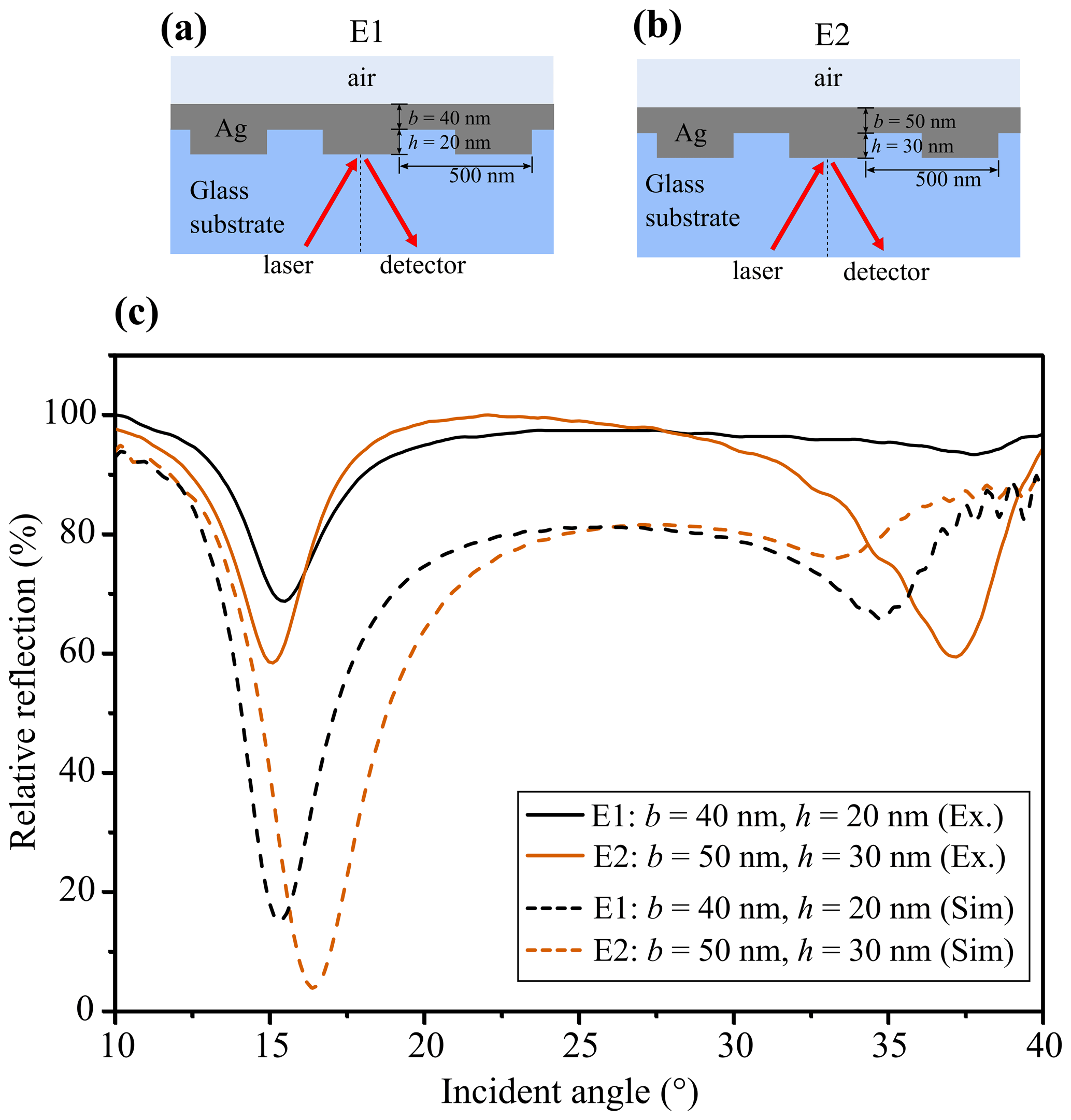
Figure 10The measurement of an inverted grating structure on a 1 mm thick glass substrate, with a 500 nm period, initially featured a 30 nm grating groove height and a 50 nm silver base thickness. Further experiments introduced variations, including a grating with a 20 nm grating groove height and a 40 nm silver base thickness. However, the results exhibited inconsistency, especially at plasmon excitation angles between different grating configurations. These disparities suggest challenges in precisely controlling and reproducing the etching processes for 20 and 30 nm grating groove height structures.
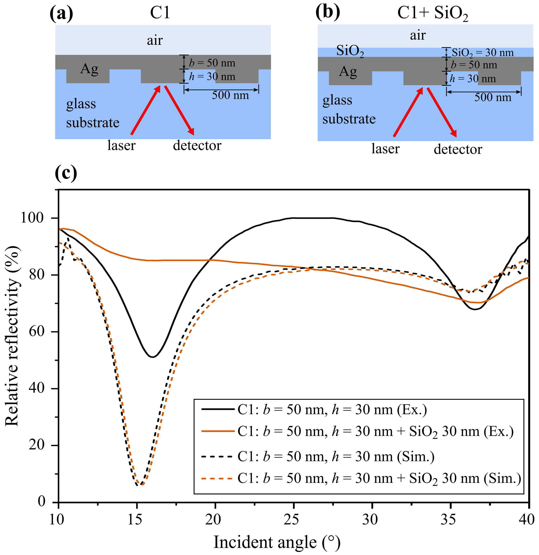
Figure 11Sketch of the inverted grating structure on a glass substrate without (a) and with (b) the silicon oxide protective layer. (c) The measurement of the inverted grating structure on the 1 mm thick glass substrate, both with and without the silicon oxide protective layer. Notably, the plasmon excitation angle exhibited a significant shift after the deposition of the silicon oxide layer. This observation suggests that high-temperature processes involved in the deposition may have affected the properties of the glass substrate and the underlying silver layer, which lacks a seed layer for controlled growth.
One possible explanation for this deviation lies in the refractive index mismatch between the substrate and the metal layer. In the simulation, this index matching is often assumed, but in real-world fabrication, achieving a perfect match can be challenging. This mismatch can lead to alterations in the plasmon excitation angle, as observed in the experimental results.
The −2-order plasmon excitation angle is shown at 37.2° (CE = 6.6), which holds particular importance in an inverted grating configuration.
Interestingly, the experimental results did not reveal the presence of the third-order plasmon excitation angle. This discrepancy between simulation and experimentation signals the need for further refinement in both domains. It suggests that the simulation models should be updated to better reflect the intricacies of real-world fabrication processes while also highlighting potential areas for improvement in the experimental setup.
The experimental data demonstrate the feasibility of coupling light waves in an inverted grating configuration. This implies that, even with minor deviations from simulation predictions, the ability to couple light waves in this configuration opens doors to numerous applications in the fields of sensing applications and in particular the options this opens up for integrated plasmonic microsystem design.
The most promising inverted structure has been investigated further to assess the feasibility of covering the plasmonic structures with protective coatings to allow for cleaning and additional protection when operating the structures under realistic conditions. To this end, a 30 nm thick SiO2 layer has been deposited onto the silver layer. Using a grating periodicity of (500 ± 10) nm, a silver base thickness b of (50 ± 5) nm, and a grating groove height of (30 ± 5) nm, structures with and without a protective layer have been compared. The results are shown in Fig. 9 and demonstrate the difficulty in maintaining the performance of the grating coupler in terms of sensitivity.
The coupling efficacy for inverted grating structures without protective coating is 12.61, which may be compared to 34.21, which has been achieved using the same materials but with a standard SPR configuration (Sarapukdee et al., 2023). When applying the SiO2 layer, the coupling efficacy decreases to 2.27, which lowers the sensitivity to 8.5° RUI−1. The reason for this performance may lie within the dielectric properties of SiO2, which points towards the need to investigate other materials for protection (Zhang and Xue, 2019). Additionally, the poor adhesion between silver and SiO2 likely leads to a poor coupling efficiency.
Previous research (Sarapukdee et al., 2023) has demonstrated that silicon oxide can be successfully used as a protective layer by plasma-enhanced chemical vapor deposition (PECVD) at high temperatures. However, for the inverted grating structure with glass–silver contact, the difference in thermal expansion coefficients between the glass substrate and the silver grating at high temperatures might cause structural integrity issues, resulting in sensor performance degradation. Depositing a protective layer of silicon oxide at lower temperatures may assist in mitigating this problem. Furthermore, future research should include the investigation of alternative low-temperature deposition methods for silicon nitride, which is another promising material for use as a protective layer due to its compatibility with the underlying silver grating structure and potential to improve sensor performance and longevity.
The inverted grating structure offers compelling operational benefits, though it is not yet as potent in coupling as conventional grating couplers. It excels in mitigating surface oxidation, prolonging the grating's lifespan and making it ideal for various practical applications. Traditional plasmonic devices are prone to corrosion and deterioration of the grating structure itself. Using the inverted grating approach, protective substrate layers and smooth, cleanable interfaces with the analyte samples may be implemented, which reduces maintenance needs and potentially cuts costs. To optimize this configuration, integrating an antireflection layer on the glass substrate is a promising approach. This innovation can substantially reduce interference from the glass, enhancing performance and possibly enabling thinner glass substrates. However, further investigation and refinement are essential for improving coupling efficacy. Ensuring robust adhesion of the silver layer to the glass is critical, especially in demanding applications. Advanced fabrication techniques and materials should be explored. Efficiency in signal detection is another area for possible improvement. While backside illumination has been explored, it still relies on complex optical systems. An exciting avenue is electrical detection through integrated circuits (Saito et al., 2019a, b) and sensors (Lin et al., 2018), streamlining the device. Additionally, integrating semiconductor nanostructures into the inverted grating presents intriguing possibilities. These nanostructures can serve as sensitive optical sensors, offering precision and sensitivity in various applications. In conclusion, while the coupling effect of inverted grating structures may not match the conventional configuration, it brings operational advantages and device design options. Preventing oxidation, improving adhesion, and exploring new detection methods are promising directions for future research and development.
Data sets are made available on request from the correspondence author (stefan.palzer@tu-dortmund.de).
Conceptualization: PS and DS; methodology: PS; software: PS; writing: SP and PS; supervision: SP. All the authors have read and agreed to the published version of the manuscript.
The contact author has declared that none of the authors has any competing interests.
Publisher’s note: Copernicus Publications remains neutral with regard to jurisdictional claims made in the text, published maps, institutional affiliations, or any other geographical representation in this paper. While Copernicus Publications makes every effort to include appropriate place names, the final responsibility lies with the authors.
We thank Philipp Czyba of TU Dortmund for providing valuable guidance on cleanroom facilities and measurement equipment.
This paper was edited by Bernhard Jakoby and reviewed by two anonymous referees.
Archambeault, B., Brench, C., and Ramahi, O. M.: The Finite-Difference Time-Domain Method, in: EMI/EMC Computational Modeling Handbook, Springer, Boston, MA, 35–70, https://doi.org/10.1007/978-1-4615-1557-9_3, 2001.
Arora, P., Talker, E., Mazurski, N., and Levy, U.: Dispersion engineering with plasmonic nano structures for enhanced surface plasmon resonance sensing, Sci. Rep.-UK, 8, 9060, https://doi.org/10.1038/s41598-018-27023-x, 2018.
Bérenger, J.-P.: The Two-Dimensional Perfectly Matched Layer, in: Perfectly Matched Layer (PML) for Computational Electromagnetics, Springer, Cham, 13–27, https://doi.org/10.1007/978-3-031-01696-7_3, 2007.
Dai, Y., Xu, H., Wang, H., Lu, Y., and Wang, P.: Experimental demonstration of high sensitivity for silver rectangular grating-coupled surface plasmon resonance (SPR) sensing, Opt. Commun., 416, 66–70, https://doi.org/10.1016/j.optcom.2018.02.010, 2018.
Elshorbagy, M. H., Cuadrado, A., and Alda, J.: High-sensitivity integrated devices based on surface plasmon resonance for sensing applications, Photonics Res., 5, 654–661, https://doi.org/10.1364/PRJ.5.000654, 2017.
Iqbal, T., Tabassum, H., Afsheen, S., and Ijaz, M.: Novel exposed and buried Au plasmonic grating as efficient sensors, Waves Random Complex, 32, 1571–1582, https://doi.org/10.1080/17455030.2020.1828665, 2022.
Joseph, S., Sarkar, S., and Joseph, J.: Grating-Coupled Surface Plasmon-Polariton Sensing at a Flat Metal-Analyte Interface in a Hybrid-Configuration, ACS Appl. Mater. Inter., 12, 46519–46529, https://doi.org/10.1021/acsami.0c12525, 2020.
Kong, L., Lv, J., Gu, Q., Ying, Y., Jiang, X., and Si, G.: Sensitivity-Enhanced SPR Sensor Based on Graphene and Subwavelength Silver Gratings, Nanomaterials-Basel, 10, 2125, https://doi.org/10.3390/nano10112125, 2020.
Kotlarek, D., Vorobii, M., Ogieglo, W., Knoll, W., Rodriguez-Emmenegger, C., and Dostálek, J.: Compact Grating-Coupled Biosensor for the Analysis of Thrombin, ACS Sensors, 4, 2109–2116, https://doi.org/10.1021/acssensors.9b00827, 2019.
Kuo, W.-K., Tongpakpanang, J., Kuo, P.-H., and Kuo, S.-F.: Implementation and phase detection of dielectric-grating-coupled surface plasmon resonance sensor for backside incident light, Opt. Express, 27, 3867–3872, https://doi.org/10.1364/OE.27.003867, 2019.
Levi, A. F. J.: Essential classical mechanics for device physics, Version: 20160901, IOP concise physics, Morgan & Claypool Publishers, ISBN 978-1681744124, 2016.
Li, D. and Sarris, C. D.: FDTD lattice termination with periodic boundary conditions, in: 2009 IEEE MTT-S International Microwave Symposium Digest, Boston, MA, USA, 7–12 June 2009, IEEE, 329–332, https://doi.org/10.1109/MWSYM.2009.5165700, 2009.
Lin, J., Li, C., Chang, C.-C., Tsai, T.-H., Zito, D., and Chang, S.-F.: Editors' Choice–Review–Semiconductor Integrated Radar for Sensing Applications, ECS J. Solid State Sci. Technol., 7, Q3126–Q3142, https://doi.org/10.1149/2.0181807jss, 2018.
Lindquist, N. C., Johnson, T. W., Jose, J., Otto, L. M., and Oh, S.-H.: Ultrasmooth metallic films with buried nanostructures for backside reflection-mode plasmonic biosensing, Ann. Phys.-Berlin, 524, 687–696, https://doi.org/10.1002/andp.201200144, 2012.
Mahmud, R. A., Sagor, R. H., and Khan, M.: Surface plasmon refractive index biosensors: A review of optical fiber, multilayer 2D material and gratings, and MIM configurations, Opt. Laser Technol., 159, 108939, https://doi.org/10.1016/j.optlastec.2022.108939, 2023.
Pedrotti, F. L., Pedrotti, L. M., and Pedrotti, L. S. (Eds.): Geometrical Optics, in: Introduction to optics, 3rd edn., Cambridge University Press, Cambridge, 16–49, https://doi.org/10.1017/9781108552493.005, 2019.
Pi, S., Zeng, X., Zhang, N., Ji, D., Chen, B., Song, H., Cheney, A., Xu, Y., Jiang, S., Sun, D., Song, Y., and Gan, Q.: Dielectric-Grating-Coupled Surface Plasmon Resonance From the Back Side of the Metal Film for Ultrasensitive Sensing, IEEE Photonics J., 8, 1–7, https://doi.org/10.1109/JPHOT.2015.2509870, 2016.
Rossi, S., Gazzola, E., Capaldo, P., Borile, G., and Romanato, F.: Grating-Coupled Surface Plasmon Resonance (GC-SPR) Optimization for Phase-Interrogation Biosensing in a Microfluidic Chamber, Sensors-Basel, 18, 1621, https://doi.org/10.3390/s18051621, 2018.
Saito, Y., Yamamoto, Y., Kan, T., Tsukagoshi, T., Noda, K., and Shimoyama, I.: Electrical detection SPR sensor with grating coupled backside illumination, Opt. Express, 27, 17763–17770, https://doi.org/10.1364/OE.27.017763, 2019a.
Saito, Y., Yamamoto, Y., Kan, T., Tsukagoshi, T., Noda, K., and Shimoyama, I.: Current Detection Type SPR Sensor using AU Grating and Backside Illumination, in: 2019 IEEE 32nd International Conference on Micro Electro Mechanical Systems (MEMS), Seoul, Korea (South), 27–31 January 2019, IEEE, 452-455, https://doi.org/10.1109/MEMSYS.2019.8870819, 2019b.
Samuel, V. R. and Rao, K.: A review on label free biosensors, Biosensors and Bioelectronics: X, 11, 100216, https://doi.org/10.1016/j.biosx.2022.100216, 2022.
Sarapukdee, P., Spenner, C., Schulz, D., and Palzer, S.: Optimizing Stability and Performance of Silver-Based Grating Structures for Surface Plasmon Resonance Sensors, Sensors, 23, 6743, https://doi.org/10.3390/s23156743, 2023.
Wood, A., Barizuddin, S., Darr, C. M., Mathai, C. J., Ball, A., Minch, K., Somoskovi, A., Hamasur, B., Connelly, J. T., Weigl, B., Andama, A., Cattamanchi, A., Gangopadhyay, K., Bok, S., and Gangopadhyay, S.: Ultrasensitive detection of lipoarabinomannan with plasmonic grating biosensors in clinical samples of HIV negative patients with tuberculosis, PLoS ONE, 14, e0214161, https://doi.org/10.1371/journal.pone.0214161, 2019.
Yoon, K. H., Shuler, M. L., and Kim, S. J.: Design optimization of nano-grating surface plasmon resonance sensors, Opt. Express, 14, 4842–4849, https://doi.org/10.1364/OE.14.004842, 2006.
Zhang, H. and Xue, X.: The research progress on corrosion and protection of silver layer, SN Appl. Sci., 1, 1–8, https://doi.org/10.1007/s42452-019-0495-3, 2019.
Zhang, Y., Liu, Y., and Li, X.: Total-Field/Scattered-Field Formulation for FDTD Analysis of Plane-Wave Propagation Through Cold Magnetized Plasma Sheath, IEEE T. Antenn. Propag., 68, 377–387, https://doi.org/10.1109/TAP.2019.2938707, 2020.