the Creative Commons Attribution 4.0 License.
the Creative Commons Attribution 4.0 License.
 | 30 Aug 2024
Thin quartz resonators as a detector element for thermal infrared sensors
Agnes Eydam
Christian Hoyer
Volkmar Norkus
Frank Ellinger
Gerald Gerlach
This work describes the manufacturing technology and packaging of a single-crystal quartz sensor with a thickness of 5 µm. The temperature dependence of the resonance frequency of quartz resonators can be used for thermal radiation sensors with a high signal-to-noise ratio. The sensitive element, in the form of a bowl or a cantilever, is ion beam etched and must be able to vibrate freely. Impedance measurements show the temperature-dependent vibration of the resonators. For higher frequencies, scattering parameters are measured using a vector network analyzer. The cantilever achieves a higher vibration amplitude than the bowl, although with many secondary resonances. The temperature coefficient of the resonance frequency is determined to be around 90 ppm K−1.
- Article
(5272 KB) - Full-text XML
- BibTeX
- EndNote


Thermal radiation sensors absorb infrared radiation, which causes a temperature change in the sensing element. Depending on the physical effect used, the change in a physical quantity is usually transformed into a signal voltage. Examples include pyroelectric sensors based on a polarization change or microbolometers with a temperature-dependent resistance (Gerlach and Budzier, 2010).
Quartz resonators, on the other hand, use the temperature dependence of the resonance frequency of piezoelectric oscillators. Frequency can be measured with high accuracy and stability. These sensors are characterized by a high specific detectivity (D*) or, rather, a high signal-to-noise ratio, allowing for the detection of very small radiation fluxes. The cutting angle at which the resonator is cut from the quartz crystal defines its properties. The so-called “Y cut” has the highest temperature coefficient of the resonance frequency and is, therefore, most suitable for temperature sensors (Neubig and Briese, 1997). In Ren et al. (2011), an array of 18 µm thick Y-cut-quartz resonators was used to monitor biochemical reactions. There, the sensor array was structured by inductively coupled plasma etching. In Pisani et al. (2011), the quartz wafer was bonded to a silicon wafer with etched cavities. Afterwards, the quartz film was thinned down, and perforations were etched to create a free-standing, corner-supported detector. These quartz bulk sensors with a minimal thickness of 7 µm achieved a value of cm Hz W−1 (Ren et al., 2010).
Another approach is the use of thin films of piezoelectric materials, such as AlN or ZnO, which can be deposited by sputtering or chemical vapor deposition to achieve resonators with thicknesses below 1 µm (Breen et al., 2016; Wang et al., 2011). However, the need for a carrier substrate and the polycrystalline films limit their detectivity. A carrier substrate is an additional heat sink, resulting in a lower temperature change in the sensing element. A value of D* = 1.59×107 cm Hz W−1 was given for an AlN micro-electromechanical systems (MEMS) resonator in Li et al. (2017). In Sui et al. (2024), a 4 µm thick ceramic lead–zirconate–titanate (PZT) thin film was fabricated by wafer bonding and chemical–mechanical polishing. Its temperature coefficient of the resonance frequency is very large, at about 200 ppm K−1; however, to date, there has not been any investigation regarding the detectivity. In Li et al. (2023), terahertz detectors using MEMS resonators are discussed in detail.
Free-standing resonator structures of single-crystalline heteroepitaxial cantilevers of several-micrometer thickness were fabricated on silicon substrates. In Peiner et al. (2000), piezoelectric layers of InP or GaAs were epitaxially grown on silicon, and the cantilever structure was realized by etching the silicon in a KOH solution. In Zimmermann et al. (2006), GaN membranes were fabricated by dry etching. However, these resonator structures have not been used as temperature sensors yet. They would be another possible approach for very thin sensors with a high signal-to-noise ratio, but this approach is not pursued in our work.
Semiconductor-based MEMS resonators have several advantages, such as their potential for integration with microelectronic and other MEMS devices and high scalability in manufacturing, resulting in very low costs with respect to mass production. On the other hand, the development of a new device and the production plants in general are very expensive and unsuitable for the production of low quantities.
Our focus lies on infrared detectors with small or medium production quantities using technology known from pyroelectric detectors, in particular ion beam etching for the thinning process. Reducing the film thickness leads to a higher resonance frequency and, consequently, an increased absolute frequency change and increased sensitivity. However, the miniaturization is carried out based on single-crystal quartz, not polycrystalline thin films, due to the lower noise and the lack of requirement for an additional substrate.
The goal of this work is to improve sensor parameters that directly influence the sensitivity, such as the reduction in quartz thickness, thermal conductivity between the sensor and the environment, and the absorption coefficient. This will lead to a better signal-to-noise ratio.
For that purpose, a technological procedure for manufacturing quartz sensors with very small thicknesses in the range of 5 µm with both plate- and beam-like structures is presented in Sect. 2. After that, impedance measurements to determine the resonance frequency up to 400 MHz are described in Sect. 3. Section 4 presents the proof of the temperature coefficient of the resonance frequency.
The starting point for the fabrication of the resonator devices are quartz wafers with a size of 20 mm × 20 mm and a thickness of 500 µm (Quarztechnik Daun GmbH, Daun, Germany). They are thinned down to a thickness of 20 µm by lapping and polishing and cut into chips with a size of 4 mm × 4 mm. The chips are structured by photolithography followed by depositing thin films or by removing material. Electrode films of NiCr and Au are deposited by thermal evaporation. The electrode is reinforced in the contact area. Structures like bowl-shaped cavities and trenches are ion beam etched.
In a first step, sensors were built up with unstructured quartz chips after each technological step (lapping, polishing, and etching) to investigate their influence on the vibration, as the crystal structure may be damaged by processing its surface (Danel and Delapierre, 1991). However, our measurements showed no effect on the vibration.
After that, two sensor layouts were implemented. The layouts have to meet the following requirements:
-
The quartz membrane of the sensitive element has to be very thin. The sensitive area is defined by the overlapping parts of the front and back electrodes.
-
The thin quartz membrane has to be mechanically stabilized.
-
The vibration of the quartz resonator should be decoupled from external vibrations.
-
An additional thermal isolation is preferable because it increases the sensitivity.
The basic concept is a thin, free-standing membrane that is stabilized by a thicker carrier frame. The detailed technological steps are presented in Table 1 and Fig. 1. The two layouts are briefly outlined in the following:
-
In the first layout, the front and back electrode form a cross. The sensitive element is the overlapping part where a bowl with a thickness of 5 µm is etched in the chip (Fig. 2a). The sensors are mounted in a TO-8 package. A substrate is glued on the base, and the quartz chip is assembled on silicon rods to decouple it from external vibrations (Fig. 2c). Ideally, it should vibrate freely without environmental influences. Three rods are used for technical reasons – there is more space to contact the back electrode without a fourth rod.
-
The second layout consists of a 5 µm thin cantilever which is connected to the thicker frame by a narrow bridge (Fig. 2b). The trench between the cantilever and frame keeps the sensitive element thermally isolated. Here, the frame is firmly fixed on a carrier substrate with a deepening in the middle, leaving the cantilever versatile (Fig. 2d). This layout has been successfully used for pyroelectric LiTaO3 sensors (Norkus et al., 2014).
Some of the sensor chips were coated with a NiCr absorption layer with a thickness of 1.2 µm to improve the radiation absorption (Schossig et al., 2010).
Table 1Technological steps to manufacture quartz resonator chips.


Figure 1Schematic representation of the technological process to manufacture quartz resonator chips.

Figure 2(a, b) Sensor layouts and (c, d) packaging for quartz resonators: sensitive element as a bowl (a, c) and as a cantilever (b, d). The numbers in the figure denote the following: 1 – sensitive element; 2 – frame; 3 – trench; 4 – bridge; 5 – silicon rods; and 6 – carrier substrate. The scale bars in panels (a) and (c) also apply to panels (b) and (d), respectively.
Before the 5 µm thin quartz chips were manufactured, the technology had been tried out with 80 µm thick test chips. These chips were either kept unstructured with an electrode covering the entire surface or they had the bowl-like structure but were etched just 10 µm deep with a final thickness of 80 µm within a 90 µm thick frame.
3.1 Experimental methods
The fundamental resonance frequency of a quartz crystal vibrating in thickness shear mode is given by
where d is the thickness of the quartz plate, c is the Young modulus, and ρ is the density (Vig, 1996). The material parameters of Y-cut quartz are c = 40 GPa and ρ = 2.65 g cm−3 (Ren et al., 2010). Figure 3 shows the Butterworth–Van Dyke (BVD) equivalent circuit of a quartz resonator. It captures the mechanical behavior of the piezoelectric transducer in terms of the electrical elements. The dynamic capacitance (C1) represents the elastic compliance, and the inductance (L1) represents the effective vibrating mass of the resonator. The resonance resistance (R1) results from the damping of the vibration. C0 is the static capacitance of the crystal. L1 and C1 form a series resonant circuit; furthermore, in combination with C0, they form a parallel resonant circuit (Neubig and Briese, 1997). The quality factor (Q) of the vibration is defined as the ratio of the resonance frequency to its 3 dB bandwidth. It can be expressed with the elements of the equivalent circuit as

By measuring the complex impedance of the device under test (DUT), in this case the quartz crystal, as a function of frequency, it is possible to accurately determine its resonance frequency. The excitation frequency is varied, and the corresponding impedance values are measured. For a series resonant circuit, the magnitude will be minimal and the phase will be zero at the resonance frequency. For parallel resonance, the magnitude of the complex impedance is maximum and the phase is ±90° with a zero crossing. A vector network analyzer (VNA) or frequency response analyzer (FRA) allows one to measure complex impedance. Using a VNA at low frequencies is inappropriate because it is limited by several factors, including the signal-to-noise ratio and calibration range. Therefore, an FRA measures current and voltage using the four-terminal method in the low-frequency range. At higher frequencies, the VNA characterizes the DUT using scattering parameters (S parameters) of an electromagnetic wave as a function of frequency. The S parameters describe the ratio of the transmitted or reflected power wave to the incident wave. In the high-frequency range, the wavelength is smaller than the cable length; thus, the current and voltage are location dependent, and a simple measurement of them is no longer sufficient (Radschun, 2017). Using the VNA, the complex impedance (more accurately the complex input impedance, ) of the DUT is determined by
with a reference impedance Z0 of 50 Ω and the complex input reflection coefficient .
In this work, six quartz resonator sensors were fabricated and studied. The first two sensors with a resonator thickness of ca. 80 µm were measured with an FRA (Solartron SI 1260, Solartron Analytical, Farnborough, UK). This analyzer operates at frequencies of up to 32 MHz. The thin sensors with a thickness of approximately 5 µm were characterized with VNAs. For that, an R&S ZVL-6 device (Rohde & Schwarz, Munich, Germany) that operates in the frequency range from 9 kHz to 6 GHz was used for sensors no. 3 and no. 4. Sensors no. 5 and no. 6 were measured with an R&S ZNB8 with a frequency range from 9 kHz to 8.5 GHz. Table 2 summarizes the characteristics of the sensors and the expected resonance frequencies determined by Eq. (1). The thickness was measured with a mechanical precision feeler for the thicker sensors or with a light section microscope otherwise.
3.2 Calibration
To obtain accurate and reliable measurements of electrical characteristics and frequency response, the measuring instruments were calibrated in advance. This calibration compensated for systematic errors caused by cables, connectors, and other factors, as the according parasitic effects are not negligible, especially at higher frequencies. Calibration was carried out using the through–reflect–line (TRL) calibration method (Engen and Hoer, 1979; Williams et al., 1991). This method defines a reference plane in close proximity to the DUT that corrects for reflections and losses caused by the test setup.
Figure 4 shows the board for TRL calibration of the VNA. This calibration of the VNA with two ports, one port on each side of the DUT, consists of the following steps:
-
Through. A line of exactly known zero length is inserted between the two ports of the VNA. The zero length refers to the reference plane, which is located at the center of this line.
-
Reflect. The reflect step is used to determine the reflection characteristics of each port. This can be done using an open or short circuit. While a short circuit has a well-defined reference plane, the open circuit can have fringing effects that introduce uncertainties. The actual magnitude of the reflection does not need to be known, but the phase of this standard must be within one-fourth of the wavelength.
-
Line. The line step involves a line of a different length compared with the through standard but with the same characteristic impedance and propagation constant. Therefore, this line must have an appropriate electrical length for the frequency range of the calibration. Thus, within this frequency range, the phase difference between the through standard and the line standard should be greater than 20° and less than 160°. For the calibration board in this work, the frequency range is between 65 and 520 MHz.
-
Match. This step is an optional low-reflection termination standard used to verify correct calibration.

Figure 4Board for TRL calibration of the VNA. The numbers in the figure denote the following: 1 – open standard; 2 – short standard; 3 – match standard; 4 – line standard; 5 – measurement fixture including TO-8 package; and 6 – through standard.
3.3 Results and discussion
Figure 5 shows the magnitude and phase of the complex impedance of sensors no. 1 and no. 2 with approximately 80 µm thick quartz resonators. The maximum of the magnitude marks the resonance frequency, which is close to the expected values (see Table 2). The calculated values depend on the accuracy of the thickness measurement. The parallel resonance is much stronger than the series resonance for both sensors. The phase at resonance is φ = −47° for sensor no. 1 and φ = 0° for sensor no. 2. Outside of the resonance the phase is −90°, which corresponds to the static capacitance C0. An ideal quartz resonator would exhibit a phase jump from −90 to +90° and back, which is almost the case for sensor no. 2. Note that the equivalent circuit in Fig. 3 is only a basic model that can be extended. Both spectra show a clear peak among smaller side resonances which are more pronounced in sensor no. 1. Secondary resonances towards higher frequencies are not uncommon in the thickness shear mode (Neubig and Briese, 1997). The behavior of sensor no. 2 bears a stronger resemblance to an ideal resonator than sensor no. 1.

Figure 5Magnitude and phase of the complex impedance of (a) sensor no. 1 and (b) sensor no. 2.
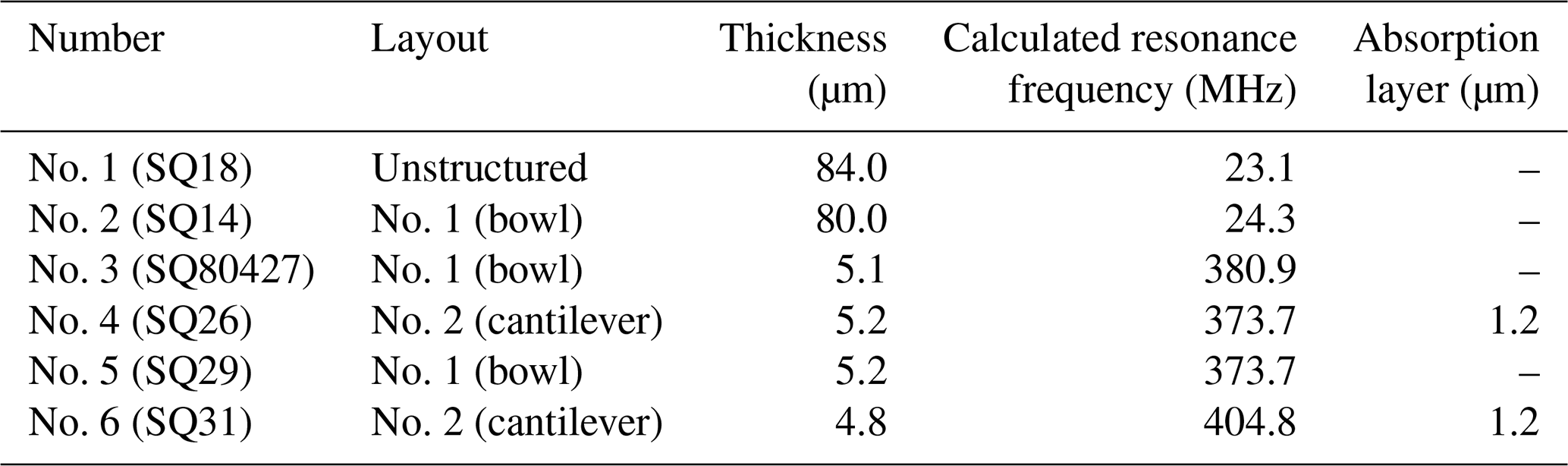
The results of sensor no. 3 are presented in Fig. 6. The spectra show the magnitude and phase of the measured parameter and the calculated impedance , respectively. The maximum of the magnitude occurs at 372.355 MHz. The resonance is explicit, but its respective amplitude and phase jump are rather small at about 1.5 dB and 20° (for ).
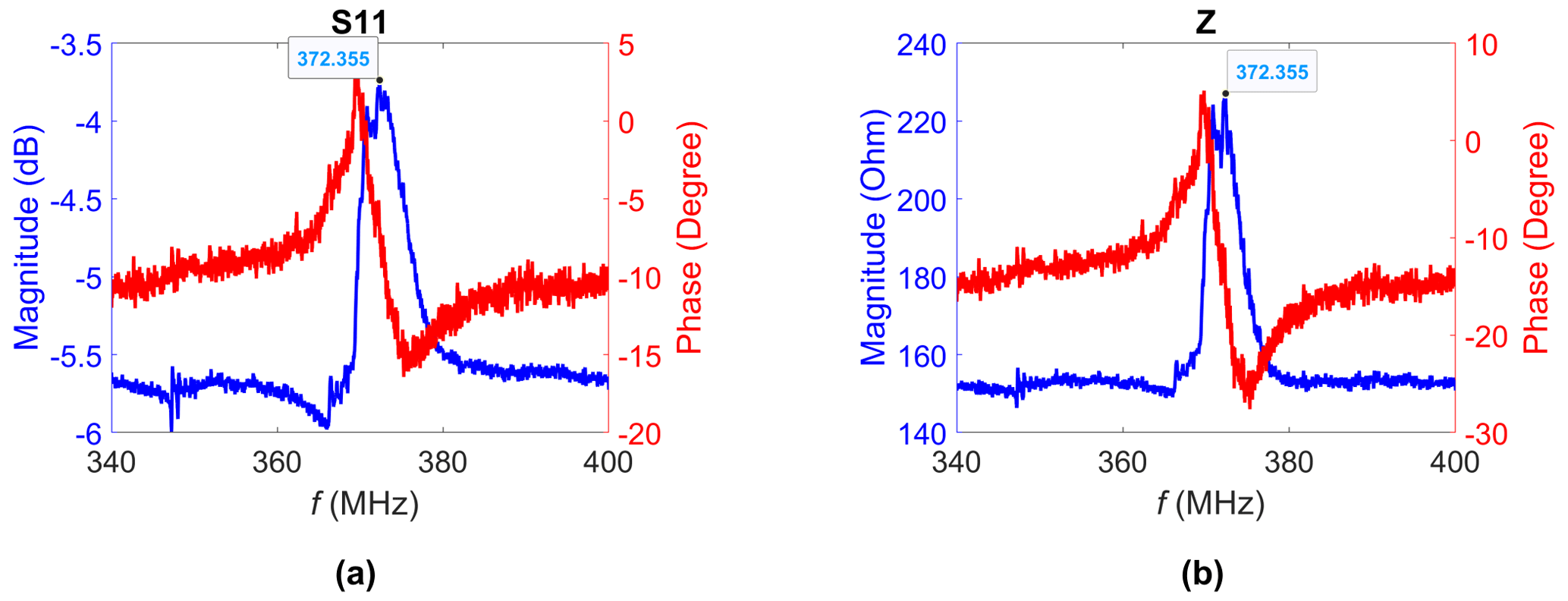
Figure 6Magnitude and phase of (a) the complex input reflection coefficient and (b) the complex impedance of sensor no. 3 (curves are smoothed). The resonance frequency is marked.
The measured impedance is fitted to the BVD model of Fig. 3. The fit in Fig. 8a reveals a quite large measurement–model disagreement. The series resonance is not visible in the measured curve. The equivalent circuit of the quartz resonator should be extended for a better fit. The quality factor amounts to 59 according to Eq. (2). An estimation using the ratio of the resonance frequency to its 3 dB bandwidth yields a value of Q = 117.
Sensor no. 4 with the cantilever achieves a vibration with a larger magnitude of approximately 8 dB and a higher phase jump of 60°, as is visible in Fig. 7a. However, the major drawback is the large number of secondary resonances. Figure 7c shows an enlarged section of the impedance spectrum in Fig. 7b. Here, both the series and parallel resonance are pronounced in contrast to sensor no. 3, which has a dominant parallel resonance. The series resonance frequency amounts to 302.5 MHz and the parallel resonance frequency to 302.75 MHz, corresponding to a resonator thickness of 6.4 µm. This value is equal to the sum of the thicknesses of the quartz chip and the absorption layer. The NiCr layer increases the mass of the resonator, resulting in a lower frequency as well known from quartz crystal microbalances (Steinem and Janshoff, 2007). This also applies to sensor no. 6 and explains the large deviation from the calculated resonance frequency.
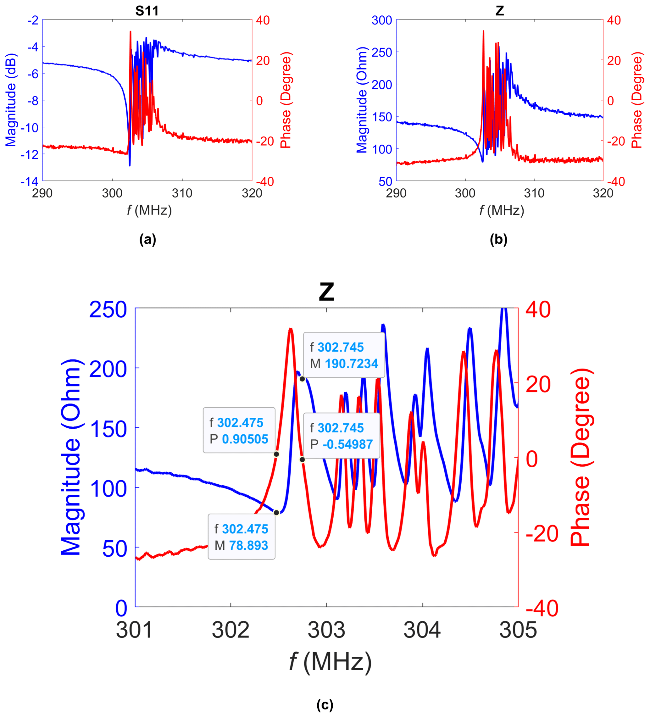
Figure 7Magnitude and phase of (a) the complex input reflection coefficient and (b) the complex impedance of sensor no. 4 (curves are smoothed). Panel (c) presents an enlarged section of panel (b); the resonance frequencies (f) and the corresponding magnitudes (M) and phase angles (P) are marked.
The fit to the BVD model for sensor no. 4 is only carried out for the main resonance, while the secondary resonances are cut off (Fig. 8b). The measurement–model agreement is moderate. The quality factor amounts to 263 using Eq. (2) and to 448 using the 3 dB bandwidth of the resonance frequency. It has improved compared with sensor no. 3, but it is extremely low with respect to the quartz resonator in Pisani et al. (2011), which has a quality factor of 4200.

Figure 8Fit of the measured impedance (magnitude) to the model of a quartz resonator in Fig. 3 for (a) sensor no. 3 and (b) sensor no. 4. The measured curve was cut off after the main resonance for sensor no. 4.
The measurements of the S parameters confirm the vibration of the 5 µm thin quartz resonators, but either the vibration amplitude is very small (sensor no. 3) or there are many side resonances (sensor no. 4). Possible approaches to improve the sensor behavior are the optimization of both the sensor packaging and the sensor layout. The quartz chip is contacted with gold wires, which are glued to the electrodes with a conductive adhesive. When mounting the chip on a carrier substrate, it is important that there is no connection between the back electrode and the substrate that could interfere with the vibration. The chip is only fixed at its four edges and should be able to vibrate freely.
To investigate the influence of the packaging, a quartz chip with a bowl (layout no. 1) was fixed on the carrier substrate with a deepening in the middle and a chip with a cantilever (layout no. 2) was positioned on silicon rods. These combinations were implemented for sensors no. 5 and no. 6 (see Table 2). Figure 9 shows the complex impedance of both sensors. The bowl in sensor no. 5 still vibrates at an unambiguous frequency, despite the stronger fixation, and the cantilever in sensor no. 6 still shows secondary resonances, although less than in sensor no. 4. Sensor no. 5 behaves similarly to sensor no. 3, and the same applies to sensors no. 6 and no. 4. This leads to the conclusion that the vibration characteristics (and thus the existence of side resonances) mainly depend on the sensor layout and not on the fixation.
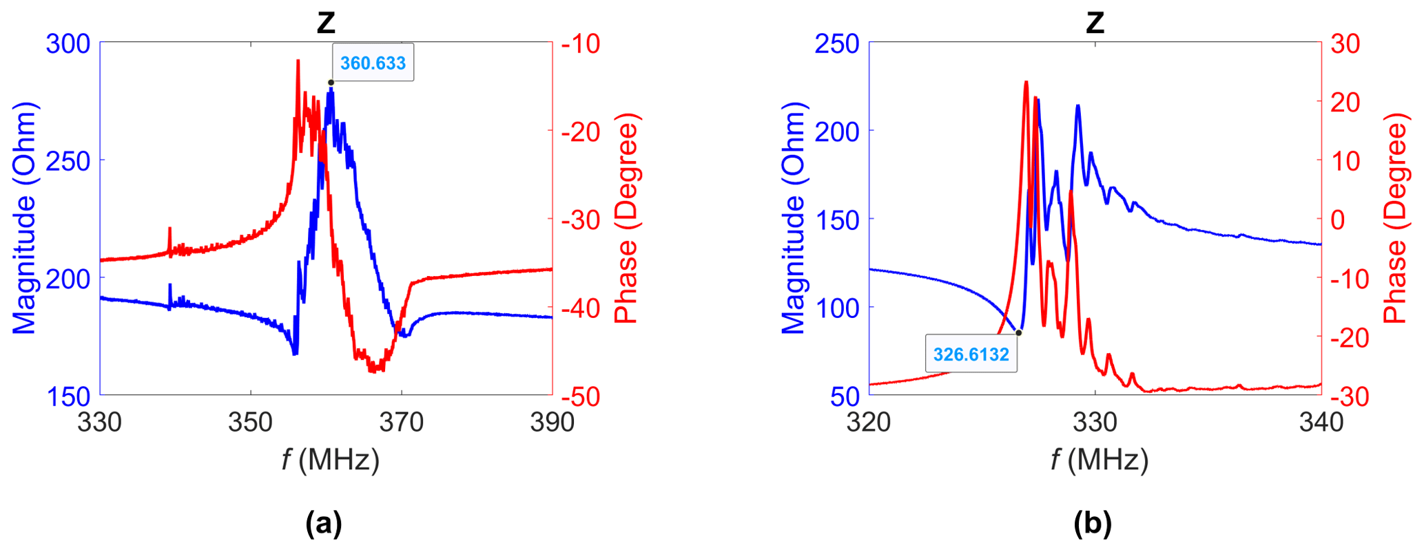
Figure 9Magnitude and phase of the complex impedance of (a) sensor no. 5 and (b) sensor no. 6. The resonance frequency is marked.
In a next step, the layout will be changed in such a way that a self-supporting quartz membrane is connected to the frame by several bridges instead of just a single one.
The targeted goal is the use of the quartz resonators as temperature sensors in the form of thermal radiation sensors. Thus, an important aspect is to validate the temperature dependence of their resonance frequency. Figure 10 shows the measurement setup.

Figure 10Measurement setup to determine the temperature dependence of the resonance frequency of the quartz resonators.
The sensor was placed in a temperature-controlled heating cabinet (WB 60K, mytron). The reference temperature was measured at the sensor cap with a PT1000 probe (GTH 175/Pt, Greisinger, Regenstauf, Germany), and the temperature of the ambient air was measured with a type-K thermocouple (YC-727, YCT Electronics, Shanghai, China). After some settling time, the temperature difference was a maximal value of 0.3 K. The S parameters were determined by the R&S ZVL-6, and the resonance frequency was derived from the calculated impedance. The chosen temperature range extended from 20 to 50 °C, as in Pisani et al. (2011). This seems reasonable for applications like the measurement of the reaction heat of biological processes.
Figure 11 presents the temperature dependence of the resonance frequency for sensors no. 3 and no. 4. It is a clear linear function. Sensor no. 3, with fr = 372.4 MHz at room temperature, shows an increase of 35.6 kHz K−1, yielding a temperature coefficient of 95.6 ppm K−1. The increase in sensor no. 4, with fr = 302.5 MHz at room temperature, amounts to 28.1 kHz K−1, yielding a temperature coefficient of 92.9 ppm K−1. This confirms the expected temperature coefficient of 90 ppm K−1 for Y-cut quartz (Neubig and Briese, 1997).

Figure 11Temperature dependence of the resonance frequency for (a) sensor no. 3 and (b) sensor no. 4.
Y-cut-quartz resonators were successfully thinned down to 5 µm by lapping, polishing, and ion beam etching. Sensors with two different layouts were built up: the sensitive element had either the form of a bowl or of a cantilever. The packaging was adjusted to the layout, ideally aiming at free vibration of the thin quartz membrane. The resonance frequency was determined by impedance measurements. A frequency response analyzer was used for sensors with a resonator thickness of 80 µm, corresponding to a frequency of around 24 MHz. Thinner quartz chips with frequencies above 300 MHz were characterized by a vector network analyzer. In the latter case, the S parameters were measured, and the impedance was calculated from them. The vibration of the quartz resonators was confirmed for both chosen sensor layouts. The sensors with a bowl-like structure show a clear resonance, but they exhibit a comparably small vibration amplitude. The cantilever vibrates with a larger amplitude but with many secondary resonances. Because the packaging does not have an effect on the side resonances, future work will focus on advancing the sensor layout.
A coupled electromechanical finite-element analysis will be implemented to analyze the influence of the chip geometry on the resonance behavior. The goal is to develop a quartz sensor with a high vibration amplitude at a clear resonance frequency with a small resonance bandwidth. Such a resonator can be excited to vibrate in an oscillator circuit. So far, this has not been successful for the 5 µm thin sensor chips.
The quartz resonators in this work are to be used as thermal radiation sensors. The temperature coefficient of their resonance frequency was determined to be approximately 90 ppm K−1 for both sensor types, as expected for Y-cut quartz. If an oscillator circuit is used, the frequency can be measured by a simple frequency counter.
All of the data in this work were generated by the authors and are available upon request.
AE and VN developed the concept of this work and chose the sensor layouts and packaging. AE designed and performed the experiments and data analysis. CH developed the calibration board for the vector network analyzer and supported the associated measurements. VN and AE were responsible for project administration. AE prepared the manuscript with contributions from CH (Sect. 3.1 and 3.2). All authors reviewed and discussed the manuscript.
The contact author has declared that none of the authors has any competing interests.
Publisher’s note: Copernicus Publications remains neutral with regard to jurisdictional claims made in the text, published maps, institutional affiliations, or any other geographical representation in this paper. While Copernicus Publications makes every effort to include appropriate place names, the final responsibility lies with the authors.
This article is part of the special issue “Sensors and Measurement Science International SMSI 2023”. It is a result of the 2023 Sensor and Measurement Science International (SMSI) Conference, Nuremberg, Germany, 8–11 May 2023.
The authors wish to thank the Deutsche Forschungsgemeinschaft (DFG) for financial support in context of the “Schwingquarzsensoren zur hochauflösenden Detektion von infraroter Strahlung” project (grant no. GE 779/44-1).
This research has been supported by the Deutsche Forschungsgemeinschaft (grant no. GE 779/44-1).
This paper was edited by Michael Kraft and reviewed by two anonymous referees.
Breen, M., Streyer, W., Lu, R., Gao, A., Wasserman, D., and Gong, S.: High speed mid-infrared detectors based on MEMS resonators and spectrally selective metamaterials, 2016 IEEE International Frequency Control Symposium (IFCS), New Orleans, LA, USA, 9–12 May 2016, IEEE, 1–6, https://doi.org/10.1109/FCS.2016.7546721, 2016.
Danel, J. and Delapierre, G.: Quartz: a material for microdevices, J. Micromech. Microeng., 1, 187–198, https://doi.org/10.1088/0960-1317/1/4/001, 1991.
Engen, G. F. and Hoer, C. A.: Thru-Reflect-Line: An improved technique for calibrating the dual six-port automatic network analyzer, IEEE T. Microw. Theory, 27, 987–993, https://doi.org/10.1109/TMTT.1979.1129778, 1979.
Gerlach, G. and Budzier, H.: Thermische Infrarotsensoren: Grundlagen für Anwender, Wiley-VCH, ISBN: 978-3-527-40960-0, 2010.
Li, C., Zhang, Y., and Hirakawa, K.: Terahertz detectors using microelectromechanical system resonators, Sensors, 23, 5938, https://doi.org/10.3390/s23135938, 2023.
Li, X., Liang, J., Zhang, H., Yang, X., Zhang, H., Pang, W., and Zhang, M.: Resonant and resistive dual-mode uncooled infrared detectors toward expanded dynamic range and high linearity, Appl. Phys. Lett., 110, 263502, https://doi.org/10.1063/1.4990285, 2017.
Neubig, B. and Briese, W.: Das große Quarzkochbuch, Franzis-Verlag, ISBN: 3-7726-5853-5, 1997.
Norkus, V., Schossig, M., Gerlach, G., Köhler, R., and Hofmann, G.: Pyroelektrische Infrarotsensoren mit hoher spezifischer Detektivität, tm – Technisches Messen, 81, 99–106, https://doi.org/10.1515/teme-2014-1018, 2014.
Peiner, E., Fricke, K., Behrens, I., Bakin, A., and Schlachetzki, A.: Hetero-micromachining of epitaxial III/V compound semiconductors, Sensor. Actuat. A-Phys., 85, 324–329, 2000.
Pisani, M., Ren, K., Kao, P., and Tadigadapa, S.: Application of micromachined Y-cut-quartz bulk acoustic wave resonator for infrared sensing, J. Microelectromech. S., 20, 288–296, 2011.
Radschun, M.: Fundamentals of vector network analyzers for impedance spectroscopy, in: Advanced School on Impedance Spectroscopy, TU Chemnitz, Chair for Measurement and Sensor Technology, 177–197, 2017.
Ren, K., Pisani, M. B., Kao, P., and Tadigadapa, S.: Micromachined quartz resonator-based high performance thermal sensors, IEEE Sensors 2010 Conference, Waikoloa, HI, USA, 1–4 November 2010, IEEE, 2197–2201, https://doi.org/10.1109/ICSENS.2010.5690612, 2010.
Ren, K., Kao, P., Pisani, M., and Tadigadapa, S.: Monitoring biochemical reactions using Y-cut quartz thermal sensors, Analyst, 136, 2904–2911, 2011.
Schossig, M., Norkus, V., and Gerlach, G.: Infrared responsivity of pyroelectric detectors with nanostructured NiCr thin-film absorber, IEEE Sens. J., 10, 1564–1565, 2010.
Steinem, C. and Janshoff, A. (Eds.): Piezoelectric Sensors, in: Springer Series on Chemical Sensors and Biosensors, Springer, https://doi.org/10.1007/b100347, 2007.
Sui, W., Kaisar, T., Wang, H., Wu, Y., Lee, J., Xie, H., and Feng, P.: Micromachined thin film ceramic PZT multimode resonant temperature sensor, IEEE Sens. J., 24, 7273–7283, 2024.
Vig, J., Filler, R., and Kim, Y.: Uncooled IR imaging array based on quartz microresonators, J. Microelectromech. S., 5, 131–137, https://doi.org/10.1109/84.506201, 1996.
Wang, Z., Qui, X., Chen, S. J., Pang, W., Zhang, H., Shi, J., and Yu, H.: ZnO based film bulk acoustic resonator as infrared sensor, Thin Solid Films, 519, 6144–6147, https://doi.org/10.1016/j.tsf.2011.03.134, 2011.
Williams, D. F., Marks, R. B., and Davidson, A.: Comparison of on-wafer calibrations, 38th ARFTG Conference Digest, San Diego, CA, USA 5–6 December 1991, IEEE, 68–81, https://doi.org/10.1109/ARFTG.1991.324040, 1991.
Zimmermann, T., Neuburger, M., Benkart, P., Hernández-Guillén, F. J., Pietzka, C., Kunze, M., Daumiller, I., Dadgar, A., Krost, A., and Kohn, E.: Piezoelectric GaN sensor structures, IEEE Electr. Device L., 27, 309–312, 2006.