
the Creative Commons Attribution 4.0 License.
the Creative Commons Attribution 4.0 License.
 | 02 Sep 2026
Modeling and extraction of residual stresses in some MEMS multilayer systems

Frank Long
Bernhard Schwartz
Geert Brokmann
Thomas Ortlepp
The intrinsic stresses introduced during the MEMS multilayer deposition process and the thermal stresses introduced during operation can significantly impact the performance, reliability, and lifetime of the product. The mechanical properties of the MEMS multilayer system are analyzed. An accurate closed-form solution is obtained for the multilayer system, including both intrinsic stresses and thermal stresses, and validated by numerical FEM simulation. Thin films are deposited on silicon substrates, and wafer bending measurements are carried out. Based on this formalism, the residual stresses in various multilayer systems are extracted and analyzed using parameter estimation theory.
- Article
(891 KB) - Full-text XML
- BibTeX
- EndNote


Residual stress is the stress that exists in an equilibrium solid without external loads. Physically, it is the sum of interatomic forces and the momentum flux intercepted by a (microscopically big) area element, divided by its area (Subramaniyan and Sun, 2008). There are intrinsic and extrinsic residual stresses. Intrinsic residual stresses include stresses induced by lattice mismatch, plastic deformation, grain growth, and other processes. Extrinsic residual stresses are induced by changes in external environmental conditions, such as temperature or humidity, and are reversed when these conditions return to their original values. The generation and evolution of residual stresses have very different origins at many different scales. They can have microscopic origins, such as point defects in solids, or mesoscopic origins, such as dislocations, grain boundaries, grains, and inclusions. They can also have macroscopic origins, such as inhomogeneity.
Residual stresses in MEMS structures can affect the reproducibility, product lifetime, and reliability of the devices because they can modify the structural, electrical, and optical properties of many MEMS materials. Residual stresses can also affect the yield of the MEMS production process because they can distort the wafers and chips. The measurement of residual stresses is therefore very important (Dutta and Pandey, 2021). Measurement methods include the X-ray method, Raman spectroscopy method, microscopic FIB method, and wafer bow method (Abadias et al., 2018; Huff, 2022). The recent cross-sectional nano-diffraction method uses an X-ray beam with a diameter of 50 nm, which can resolve the stress gradients and measure the stress in thin films (Zeilinger et al., 2016). The X-ray method measures residual strain. To calculate the residual stress, Young's modulus is also used, like in the wafer bow method (Freund and Suresh, 2010). One limitation of this method is that it is not suitable for amorphous films. Raman spectroscopy can extract the residual stress from the Raman shift of the specific lattice vibration spectral line. The deformation potential involved in the extraction must be calculated or calibrated (Ma et al., 2021). This method is not useful for amorphous films (Huff, 2022). MEMS technology involves many thin films. The most frequently used films, such as thermal oxide, CVD-deposited oxide, and nitride films, are amorphous. Therefore, the wafer bow measurement method is widely used for MEMS technology due to its non-destructive nature and ease of integration into the manufacturing process. Wafer bow measurements can be taken using the 3D laser line scanning method (Schlarp et al., 2018) or a simple two-laser beam set-up (Janssen, 2007).
The kinetic evolution of residual stresses in multicrystalline films has been systematically investigated (Engwall et al., 2016, and Chason et al., 2012). The results show a general tendency toward tensile stress due to the grain growth in the initial stage and compressive stress due to the net flux of atoms into the top of the grain boundary during film growth in the latter stage (Chason et al., 2018). The formation and evolution of residual stresses in amorphous films are more complex and dependent on the growth process and history (Murry, 1994 and Chen et al., 2003). Therefore, a convenient residual stress-monitoring and evaluation method would be useful.
While the mechanical properties of multilayer systems can be numerically simulated through finite-element analysis, the modeling of realistic structures, such as large wafers composed of multiple thin layers with high aspect ratios, requires substantial computational resources. Its application to process optimization is even more demanding. Hence, an analytical solution is desirable. Stoney's formula (Stoney, 1909) of the bending of a double metal layer due to residual stresses from manufacturing was the first development in this direction and has led to the application of this geometrical method in many fields. For extrinsic residual stresses, i.e., thermal stresses, this theory has been extended to multilayer structures (Obata, 2014; Shi et al., 2022). For intrinsic residual stresses, an equivalent reference temperature (ERT) technique has been developed and combined with laminate theory to model multilayer structures (Nejhad et al., 2003). In this paper we extend these formalisms to more general cases, including both intrinsic residual stresses and thermal stresses in multilayers simultaneously. The equilibrium conditions and continuity of strains in multilayer systems are used to derive the solution. Instead of the general anisotropic constitutive equation used in Nejhad et al. (2003), a linear isotropic elastic property is assumed. This leads to an accurate closed-form solution. This approach can be conveniently used to extract residual stresses in multilayer systems and optimize the MEMS production process flow.
Assuming that the residual stresses of underlying layers will not change during the deposition or etching of new layers, a methodology is proposed to extract residual stresses from multiple wafer bow measurements. Various multilayer structures are realized through successive deposition or successive etching. The wafer bows are measured using 3D laser line scanning, and the residual stresses in the different layers are extracted using the developed formalism. Unlike the X-ray and Raman spectroscopy methods, which can extract stresses without layer geometry information, this model requires layer thickness and wafer size to be known. Because possible errors exist in the involved layer thicknesses, wafer bow measurements, and layer properties, we apply a parameter estimation theory to our formalism to study error propagation and parameter precision. Finally, the formalism, the residual stress extraction methodology, its potential applications, and the residual stresses extracted for the various layers are discussed.
2.1 General multilayer system
We consider a beam with a multilayer structure of n layers with Young's modulus Ei, Poisson's ratio νi, thermal expansion coefficient (TEC) αi, intrinsic residual stress σi, and homogeneous thickness hi for layer i, where . Due to the residual stresses presented in the layers, the multilayer structure may experience a bending with radius R to balance the residual stresses. The origin of the y axis is at the bottom of the first layer (Fig. 1). The system is supposed to be at a temperature ΔT above the reference temperature Tr. Then, in the isotropic linear elastic approximation, the elastic stress σxi at layer i can be expressed as
where is the curvature of the bent structure, and ϵ0 is the net strain. For a circular wafer with cylindrical symmetry, the biaxial modulus is used for Ei. According to the virtual work principle, the system satisfies the equilibrium conditions of the total force and bending moment (Obata, 2014). Solving the equilibrium equations, we obtain the following two parameters:
where
2.2 Simplification in special cases
For a two-layer system, n=2, one obtains the following at the reference temperature, ΔT=0:
Furthermore, for a single thin film deposited on a substrate at the reference temperature, if the top layer (i=2) is much thinner than the substrate (i=1), i.e., h2≪h1, and the substrate is free of residual stress, σ1=0, the above formula is reduced to the Stoney formula.
A situation of interest is a thin multilayer on a thick substrate. If n thin layers are deposited on a residual-stress-free substrate with Young's modulus Es and thickness hs, such that , then
The average elastic stress in layer i is approximately
where Ft and Mt are the total linear force density and the total linear moment density of the thin-layer system:
with yic being the center position of thin layer i. This can be used in the sensor design to optimize the chip deformation and elastic stress in the function layer. It can also be used to design optical thin-film interference filters. By adjusting the thickness and residual stress of the individual films, a flat filter can be ensured. This is because the alternative tensile and compressive residual stresses can be compensated for to achieve a small curvature.
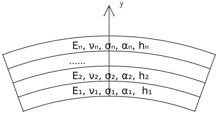
Figure 1 The bent multilayer structure of n layers with corresponding elastic parameters Ei,νi, residual stresses σi, the thermal expansion coefficient αi, and thickness hi. The bending radius is R.
2.3 Validation of the theory
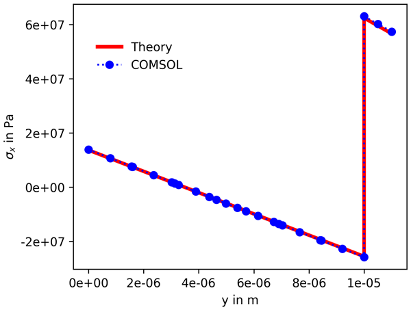
To verify the theory, we simulate a double-layer cantilever composed of a 10 µm silicon layer and a 1 µm nitride layer with COMSOL. The cantilever is 200 µm in length. Assuming a residual stress of 1×10⁸ Pa in the nitride layer, we obtain the elastic distribution at position x=90 µm, as shown in Fig. 2. According to the Saint-Venant principle, the effects of the boundary constraints can be neglected in a region sufficiently far from the boundary (von Mises, 1945). This elastic stress distribution can be compared with the results calculated using our theory (Fig. 2), demonstrating good agreement between the calculated and simulated results.
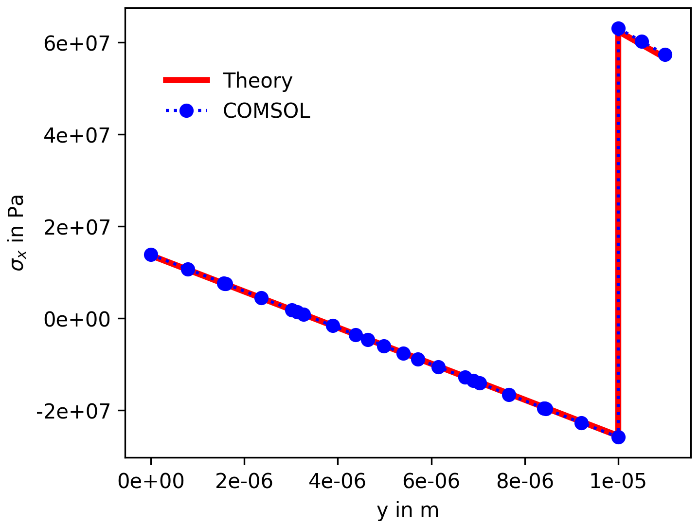
Figure 2 The elastic stress distribution in the double layer simulated with this theory (red line) and with COMSOL (dotted blue line).
The equibiaxial residual stress problem in a deposited circular wafer is axisymmetric. It can be shown that the 2D-axisymmetric problem is equivalent to the beam problem from the previous section, with the symmetric center at at the fixed end of the beam (Timoshenko and Goodier, 2010). The same formalism (Sect. 2.1) for the beam can be applied, with the axial residual stress interpreted as the value of the equibiaxial stress. In MEMS technology, many implantations, depositions, and annealing processes are involved. These processes induce residual stresses, resulting in wafer bending and chip deformation. This formalism can be used to ensure that the wafer bow remains within the process tolerance throughout the entire process flow by optimizing the film thickness and process parameters. To do so, the process-dependent residual stresses must be known. This can be achieved through the inverse problem of the formalism by starting with the measured wafer curvature and deducing the residual stresses.
3.1 Extraction of residual stresses of the multilayer system
If the residual stresses are kept constant after deposition, they can be extracted with wafer bow measurements. We consider a MEMS structure involving n layers with l unknown residual stresses that need to be extracted. Then, l≤n, because the residual stress in some layers may be known or assumed to be stress free. One designs an experiment with m wafers with different layer structures from the same process flow. These different film-stacking structures can be achieved by inserting or taking out wafers from the same process flow. This is the successive deposition approach, where the deflection of each deposited wafer is measured. The same can be achieved after the entire process by etching the deposited wafer layer by layer. This is the successive-etching approach, where the deflection of each etched wafer is measured. This yields a data set of m measurements. The flat wafer bends due to the residual stress of the deposited thin films. The bending profile can be approximated by a spherical cap with curvature κ. The wafer center shifts a deflection g (wafer bow) relative to the wafer rim. The deflections of the wafers are measured using 3D laser line scanning based on the principle of optical triangulation (Schlarp et al., 2018). For a wafer of diameter d, one can obtain the deflection from the bending curvature (κ) as
if the bending radius is much bigger than the wafer size. One can thus get m equations for the l unknown residual stresses. The residual stress of a given layer is assumed to be the same when it appears in different combinations of layer stacks because it is formed in the same process and under the same conditions. With an optimization method, one can extract the l residual stresses if m is bigger than or equal to l. A Python program was written for data analysis. The fsolve and minimize functions of the scipy module optimize are used for stress extraction in the cases of m=l and m>l, respectively.
This formalism can be generalized to analyze inhomogeneous residual stresses in a multilayer system. In this case, small cantilever test structures should be implemented on the wafer. In Huber et al. (2026), cantilevers were fabricated, and the local residual stress in a single overlay was analyzed using the Stoney formula. Our formalism can be applied to a multilayered cantilever by replacing the wafer radius with the cantilever length. Instead of using the biaxial modulus for the wafer bow, the original Young's modulus should be used for the cantilever deflection.
3.2 Parameter error estimation
The precision of the fitted residual stress depends not only on the fitting residuals themselves, but also on the measurement errors of deflection and thickness, as well as the parameter errors of Young's modulus and the thermal expansion coefficient of the films. Here, we neglect the effect of possible uncertainties in Poisson's ratios. These errors can propagate to the uncertainty in the extracted residual stresses. For measurement j, the theoretical deflections are
The total standard deviation of deflection δt(gj) is therefore
where res(gj) is the fitting residual, which directly determines the fitting error; δ(gj) is the measurement error of the deflection of the jth measurement; δ(hi) is the thickness error of the ith layer; and δ(Ei) and δ(αi) are the parameter errors of Young's modulus and the thermal expansion coefficient of the ith layer, respectively. They determine the propagated error of the fitted residual stresses. One can obtain the uncertainties in the l fitted unknown residual stresses from sensitivity analysis (Cowan, 1998). The m×l Jacobian matrix J, also known as the sensitivity matrix, can be calculated numerically with the following elements:
The l×l Fisher information matrix of the fitted parameters is approximately (Ober et al., 2003)
where
The inversion of Fisher's information matrix is the covariance matrix C of fitting parameters . The standard deviations, the correlation matrix, and the confidence intervals of the fitted residual stresses can be calculated from the covariance matrix (Tarantola, 2005). The relative error of the kth fitted residual stress is
With nonzero errors, δ(gj), δ(hi), δ(Ei), and δ(αi), one can see the error propagation.
3.3 Residual stress extraction with successive deposition method
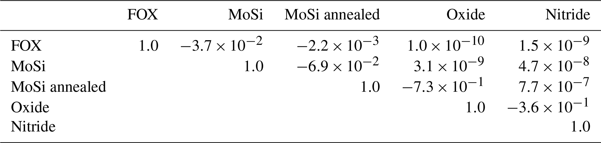
We designed an experiment (experiment I) to study the residual stresses of four thin films – oxidation layer (FOX), MoSi, CVD oxide, and stress-reduced LPCVD nitride – to investigate the generation and evolution of residual stresses in different layers involved in a MEMS production process. Since the MoSi layer will be annealed, we designed a five-step experiment using five starting wafers of (100)-Si with a thickness of 390 µm. After the thermal oxidation process, wafer 1 was removed from the flow. A MoSi layer was then deposited on the remaining wafers, after which wafer 2 was removed from the flow. The remaining three wafers were annealed, and wafer 3 was removed from the flow. LPCVD oxide deposition was performed on the remaining two wafers, after which wafer 4 was removed from the flow. Finally, a stress-reduced LPCVD nitride deposition was performed on wafer 5. The process steps and the wafers used are shown in Table 1. The wafer bows of the five wafers with different layer stacking were measured using 3D laser line scanning. As an example, Fig. 3 shows the wafer scans for wafer 2 (with the MoSi layer as deposited) and wafer 3 (after high-temperature annealing of the deposited MoSi layer). The wafer bending profiles aligned well with the arc of a circle, except for the rim of the wafer. This agrees with the Saint-Venant principle. This demonstrates that the curvature can be easily calculated from wafer deflection using Eq. (15). The results indicate that the stress in the MoSi layer changed drastically after annealing. The mechanical properties of the layers involved in this paper are shown in Table 2. For stress extraction, the wafer bows shown in Table 1, which have been corrected with the initial wafer bow, are used. Using the error analysis theory (Sect. 3.2), we calculated the relative fitting errors with ideal experimental parameters and the total relative errors, which took into account the propagated error from the 1 % relative error in wafer deflection, and the same relative error in thickness, Young's modulus, and the thermal expansion coefficient of all involved layers. The layer thicknesses, the extracted residual stresses, the relative fitting errors, and the total relative errors of fitted residual stresses are shown in Table 3. The results show that the residual stress of oxide depends on the preparation method and preceding layers. The exact kinetics are still unknown and must be studied using more systematic technological parameters. Furthermore, the correlation matrix of the fitted parameters is shown in Table 4, which also includes the propagated errors. A large anticorrelation coefficient is observed between the residual stresses of annealed MoSi and oxide. Although the total relative error of the fitted parameters is small, this correlation distorts the confidence ellipse from an ideal circle and will increase the size of the profile confidence interval (Jeyaratnam, 1992).
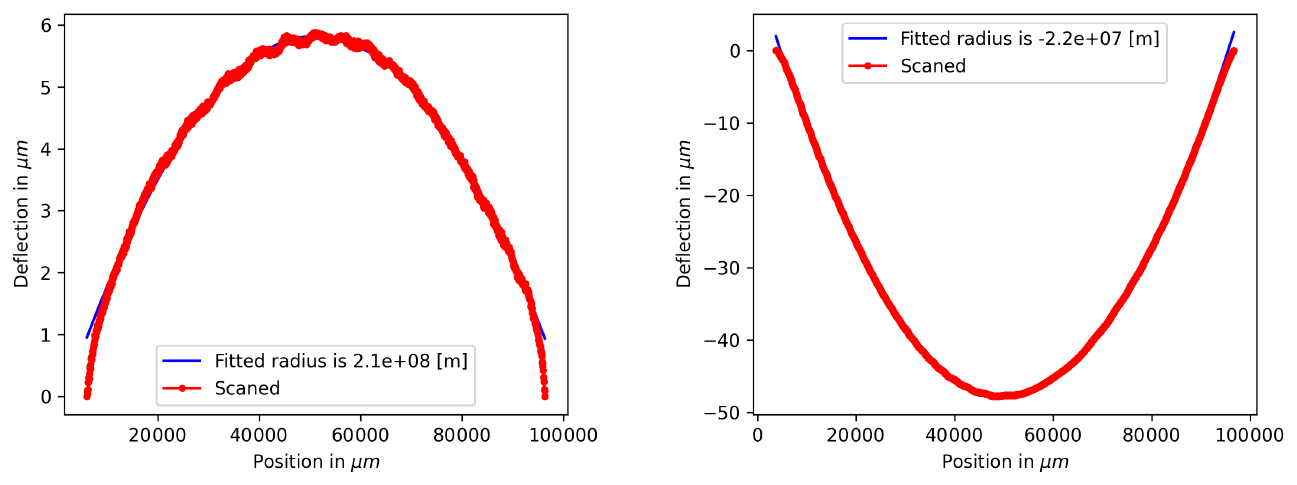
Figure 3 The wafer profile measured using laser scanning (dotted red line) and the fitting to an arc (blue line) for wafer 2 (left) and wafer 3 (right). Wafer 2, with an as-deposited MoSi layer, exhibits tensile stress. Wafer 3, with an annealed MoSi layer at 1000 °C for 30 min, shows a compressive stress.
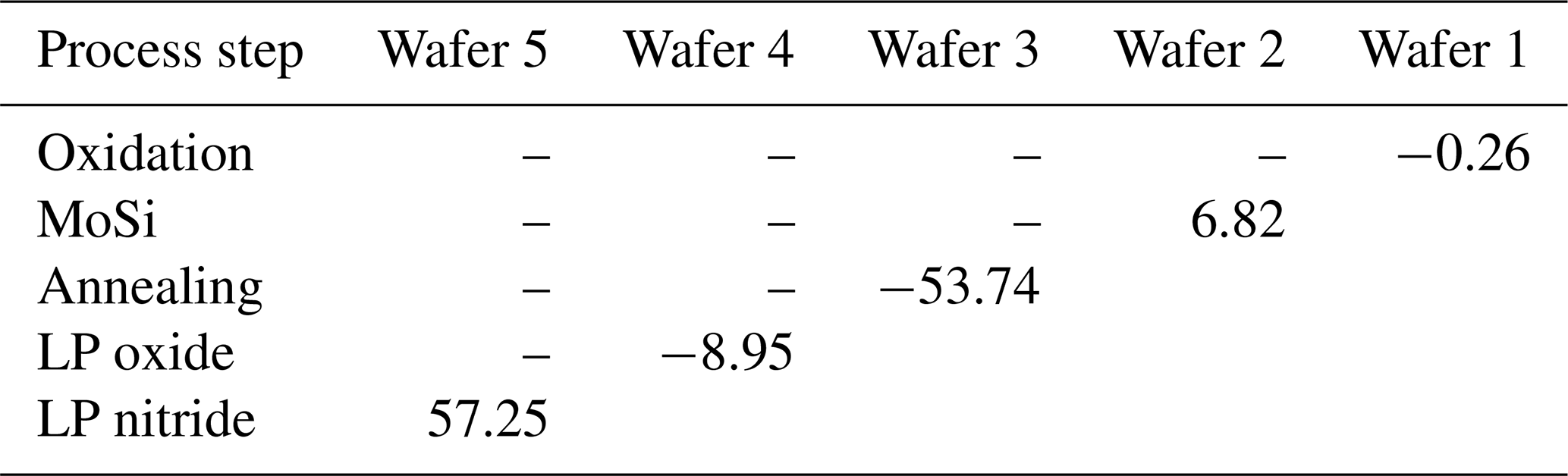
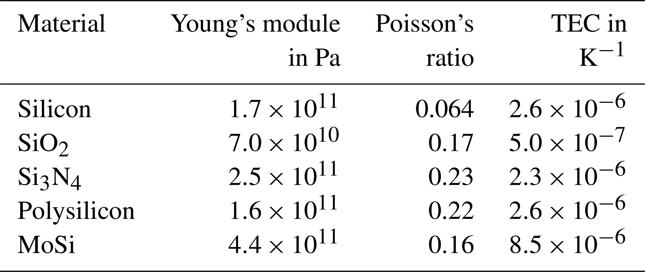
Table 3Layer thicknesses, extracted residual stresses, relative fitting errors, and total relative errors of the extracted residual stresses of experiment I.
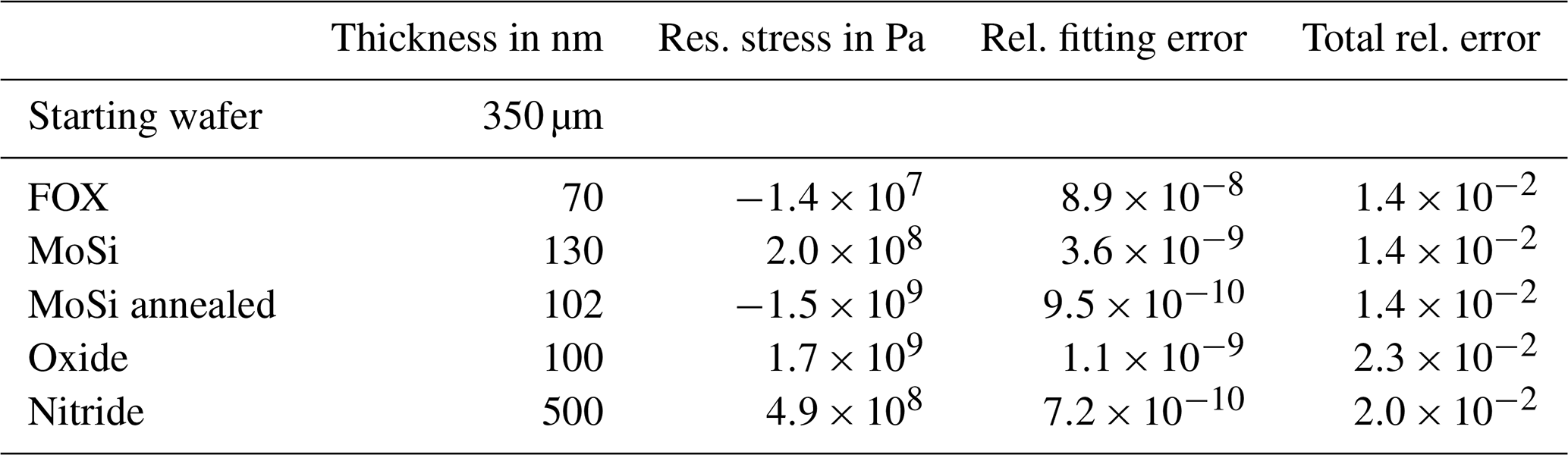
Table 4Symmetrical correlation matrix of the extracted residual stresses of experiment I.
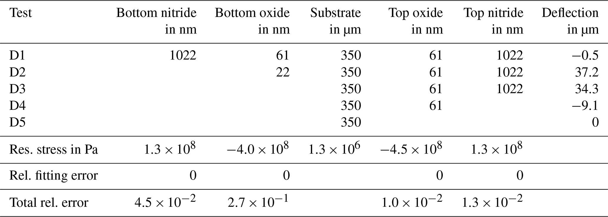
3.4 Residual stress extraction with successive-etching method
For experiment II, we start from a 100 mm diameter n-type (100) silicon wafer, which was oxidized with 60 nm silicon dioxide and deposited with 1 µm silicon nitride with LPCVD. The silicon nitride layer was deposited with a high DCS(dichlorosilane):NH3 flow ratio to effectively reduce the residual stress (Zheng et al., 2013). To extract the residual stress in the thin layers, the layer thickness and wafer bow are measured at different stages of multilayer etching. The first bow measurement, D1, was made for the initial processed wafer without any etching. The second bow measurement, D2, was made after the backside nitride layer was removed. The third bow measurement, D3, was made after the backside oxide layer was removed. The fourth bow measurement, D4, was made after the topside nitride layer was removed. Finally, the fifth bow measurement, D5, was made after the topside oxide layer was removed. The experimental results, the extracted residual stresses, the relative fitting errors, and the total relative errors in the fitted residual stresses (as in Sect. 3.3) are shown in Table 5. The results show that the relative fitting error is very small. The fitted residual stress of the nitride film, 1.3×10⁸ Pa, agrees well with the value of 1.35×10⁸ Pa presented in Zheng et al. (2013). This also confirms the effectiveness of the high DCS:NH3 ratio in reducing the residual stress of LPCVD nitride films. The residual stresses of normal LPCVD nitride films is 1.3×10⁹ Pa (Sect. 3.5), while the residual stress of nitride prepared in experiment I (Sect. 3.3) is only reduced to 4.9×10⁸ Pa.
Table 5Layer thicknesses, wafer bows, extracted residual stresses, relative fitting errors, and total relative errors of the extracted residual stresses of experiment II.
3.5 Extraction of thermal stresses and intrinsic residual stresses
For experiment III, two 100 mm diameter n-type (100) silicon wafers, both 498 µm thick, are deposited with 300 nm of silicon dioxide and 100.7 nm of silicon nitride, respectively. The deposited film on the backside is etched away. The Tencor FLX2900 system is used to perform wafer curvature measurements with temperatures scanned from 50 to 350 °C. For stress extraction, it is assumed that the intrinsic residual stresses and thermal expansion coefficient (TEC) of the films remain constant during wafer heating measurements. Figure 4 shows the measured and simulated wafer curvature as a function of temperature. The fitted residual stress of silicon dioxide film is Pa, and that of silicon nitride film is 1.3×10⁹ Pa. The relative fitting errors are and for silicon dioxide and silicon nitride films, respectively. The corresponding total relative errors are and , respectively, if the propagated errors are taken into account like in Sect. 3.3. The thermal stresses are induced by the TEC differences between the film and substrate. Because the experiments contain errors in both the curvature measurement and the temperature reading, the extracted residual stresses also contain propagated uncertainty. Using these parameters, one can calculate the average elastic stress in the thin layer, as illustrated in Fig. 5.
It has been demonstrated that this formalism can address both intrinsic and extrinsic residual stresses in a layered structure. This is a useful extension of established approaches. For example, the widely used Stoney formula (Chason et al., 2018) can be applied to a single layer deposited on substrate. Thermal stresses can be analyzed in a layered structure with any number of layers (Shi et al., 2022), but intrinsic stresses induced by manufacturing are not incorporated. The equivalent reference temperature method (Nejhad et al., 2003) for dealing with intrinsic residual stresses can also model multilayer systems; however, no closed-form solution can be obtained. Therefore, it is difficult for them to be used in the reverse problem of general residual stress extraction. Furthermore, a systematic methodology for parameter extraction is presented using either successive deposition or etching methods, and a parameter estimation method is proposed. Additionally, this closed-form formalism can be incorporated into established device design flows and online stress-monitoring software as a software gadget to improve device performance and process yield.
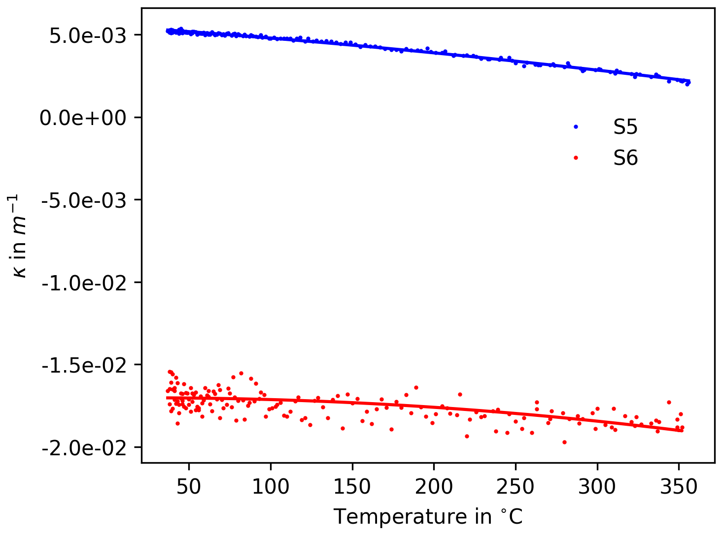
Figure 4 Experiment IV – the measured (dot) and simulated (line) curvatures at different temperatures for wafer S5 (SiO2 film, blue) and wafer S6 (Si3N4 film, red).
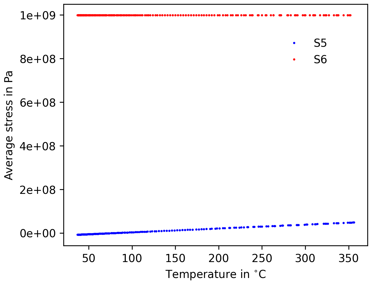
Figure 5 Experiment IV – the average elastic stresses in thin film at different temperatures for wafer S5 (SiO2 film, blue) and wafer S6 (Si3N4 film, red).
For properly designed experiments with either successive etching or successive deposition and wafer bow measurements, the residual stresses in different layers can be extracted. Except for a few special layers, the total relative errors (including all possible propagated errors) of the fitted residual stresses are reasonably small. It can be seen that, except for nitride and the as-deposited MoSi layer, all layers have compressive residual stress. The polycrystalline MoSi film exhibits compressive stress after high-temperature annealing, which agrees with the model (Chason et al., 2018). We investigated how different processes affect residual stress, especially for LPCVD nitride, and confirmed the effectiveness of the procedure suggested in Zheng et al. (2013) for reducing tensile stress.
Theoretical expressions have been derived for wafer bending of multilayer systems caused by isotropic, homogeneous residual stresses stemming from both process-induced and thermal stresses at arbitrary temperature. This is an extension of the thermal stress theory for multilayer systems (Shi et al., 2022) and the equivalent reference temperature technique for the intrinsic stresses in layered structures (Nejhad et al., 2003). A Python-based extraction procedure has been developed. Using this procedure, the residual stress in each layer can be determined from a set of wafer bow measurements. Error propagation and the total relative error are estimated for the extracted residual stresses by applying the parameter estimation theory to our cases. Although many error factors are involved in wafer bending, it has been shown that error propagation can be kept small. To improve parameter estimation, the layer structure should be chosen to minimize parameter correlation and error propagation for residual stress extraction. Once the residual stresses associated with the different process steps have been determined, the process flow and layer structure can be designed using the theory presented in Sect. 2.1. This allows the process to simultaneously achieve optimal chip performance and ensures a trouble-free flow. This increases the chance of success in a single run for the development of new devices.
In MEMS technology, layers are often patterned in periodic structures or a porous layer is applied. These form a type of metastructure. The equivalent elastic properties (Jhung et al., 2009) can be used in this formalism to carry out the wafer bow analysis. Some MEMS devices, such as microemitters, operate at high temperatures. The additional thermal stresses can accelerate electrochemical migration, influencing the stability and lifetime of the devices. Our measurements and calculations of thermal stress show that an embedded prestress can alleviate the problem. Thus, the design of microsensors and microactuators can be optimized to minimize chip bowing and maintain low elastic stresses in the functional layers under all operating conditions. This approach ensures a higher production yield and the long-term reliability of sensors and actuators.
Modern MEMS technology involves many layers in the process. To guarantee optical, electrical, and mechanical performance, process conditions are modified and optimized. This often results in the generation of residual stresses. These stresses can be modified or relaxed in subsequent processes. All of these factors make grasping residual stresses challenging. The induced wafer bow can affect process precision because lithographic steps must be performed on a deformed wafer. After processing, a deformed wafer can make the automated wafer-level test difficult. Therefore, managing residual stress generation and evolution throughout the entire process is important. On the other hand, wafer bending is a direct indicator of residual stress. The wafer bow test is a reliable, non-destructive method of measuring residual stress. The presented closed-form formalism can facilitate its application to multilayer systems. In the future, the kinetics of residual stress generation and evolution in amorphous films should be systematically investigated. In addition to the successive deposition and successive-etching procedures used for residual stress extraction, the production line should properly incorporate online measurements with quick and reliable residual stress evaluation.
The theoretical derivation, code, and data used in this study are available from the corresponding author upon request.
L. Long: theoretical derivation, F. Long: code and measurement, B. Schwartz: Tencor system measurement, G. Brokmann and T. Ortlepp: organization and discussion.
The contact author has declared that none of the authors has any competing interests.
Publisher's note: Copernicus Publications remains neutral with regard to jurisdictional claims made in the text, published maps, institutional affiliations, or any other geographical representation in this paper. The authors bear the ultimate responsibility for providing appropriate place names. Views expressed in the text are those of the authors and do not necessarily reflect the views of the publisher.
This research has been supported by the Bundesministerium für Wirtschaft und Klimaschutz (grant no. 49MF230027).
This paper was edited by Michele Penza and reviewed by two anonymous referees.
Abadias, G., Chason, E., Keckes, J., Sebastiani, M., Thompson, G. B., Barthel, E., Doll, G. L., Murray, C. E., Stoessel, C. H., and Martinu, L.: Review Article: Stress in thin films and coatings: Current status, challenges, and prospects, J. Vac. Sci. Technol. A., 36, 020801, https://doi.org/10.1116/1.5011790, 2018. a
Chason, E., Shin, J. W., Heame, S. J., and Freund, L. B.: Kinetic model for dependence of thin film stress on growth rate, temperature, and microstructure, J. Appl. Phys., 111, 083520, https://doi.org/10.1063/1.4704683, 2012. a
Chason, E., Engwall, A. M., Rao, Z., and Nishimura, T.: Kinetic model for thin film stress including the effect of grain growth, J. Appl. Phys., 123, 185305, https://doi.org/10.1063/1.5030740, 2018. a, b, c
Chen, K. S., Zhang, X., and Lin, S. Y.: Intrinsic stress generation and relaxation of plasma-enhanced chemical vapor deposited oxide during deposition and subsequent thermal cycling, Thin Solid Films, 434, 190–202, https://doi.org/10.1016/S0040-6090(03)00462-0, 2003. a
Cowan, G.: Statistical Data Analysis, Oxford University Press, ISBN 0-19850156-0, 1998. a
Dutta, S. and Pandey, A.: Overview of residual stress in MEMS structures: Its origin, measurement, and control, J. Mater. Sci. Mater. Electron., 32, 6705–6741, https://doi.org/10.1007/s10854-021-05405-8, 2021. a
Engwall, A. M., Rao, Z., and Chason, E.: Origins of residual stress in thin films: Interaction between microstructure and growth kinetics, Materials and Design, 110, 616–623, https://doi.org/10.1016/j.matdes.2016.07.089, 2016. a
Freund, L. B. and Suresh, S.: Thin Film Materials: Stress, Defect Formation and Surface Evolution, Cambridge University Press, ISBN 9780511754715, 2010. a
Huber, D., Schallert, C., Gesing, A., Steinmüller-Nethl, D., Pfusterschmied, G., and Schmid, U.: Automated contactless characterization of local thin film thickness and film stress with standard MEMS structures at wafer level, J. Sens. Sens. Syst., 15, 9–21, https://doi.org/10.5194/jsss-15-9-2026, 2026. a
Huff, M.: Review Paper: Residual Stresses in Deposited Thin-Film Material Layers for Micro- and Nano-Systems Manufacturing, Micromachines, 13, 2084, https://doi.org/10.3390/mi13122084, 2022. a, b
Janssen, G. C. A. M.: Stress and strain in polycrystalline thin films, Thin Solid Films, 515, 6654–6664, https://doi.org/10.1016/j.tsf.2007.03.007, 2007. a
Jeyaratnam, S.: Confidence intervals for the correlation coefficient, Stat. Probabil. Lett., 15, 389–393, https://doi.org/10.1016/0167-7152(92)90172-2, 1992. a
Jhung, M. J., Choi, Y. H., and Ryu, Y. H.: Equivalent Material Properties of Perforated Structure for Free Vibration Analysis, IASMiRT, ISBN 9781617820243, 2009. a
Ma, L., Zheng, J., Fan, X., and Qiu, W.: Determination of stress components in a complex stress condition using micro-Raman spectroscopy, Opt. Express, 29, 30319–30326, https://doi.org/10.1364/OE.434235, 2021. a
Murry, P. E.: Thermal strain and viscous flow of glass films, J. Appl. Phys., 76, 723–727, https://doi.org/10.1063/1.357816, 1994. a
Nejhad, M. N. G., Pan, C., and Feng, H.: Intrinsic Strain Modeling and Residual Stress Analysis for Thin-Film Processing of Layered Structures, J. Electron. Packag., 125, 4–17, https://doi.org/10.1115/1.1512295, 2003. a, b, c, d
Obata, Y.: Beams, Thermal Stresses, in: Encyclopedia of Thermal Stresses, edited by: Hetnarski, R. B., Springer, https://doi.org/10.1007/978-94-007-2739-7, 2014. a, b
Ober, R. J., Zou, Q., and Lin, Z.: Calculation of the Fisher Information Matrix for Multidimensional Data Sets, IEEE Trans. Signal Process., 51, 2679–2691, https://doi.org/10.1109/TSP.2003.816880, 2003. a
Schlarp, J., Csencsics, E., and Schitter, G.: Optical scanning of laser line sensors for 3D imaging, Appl. Optics, 57, 5242–5248, https://doi.org/10.1364/AO.57.005242, 2018. a, b
Shi, Y., Xu, J., Li, Y., Liu, Z., Zhang, K., and Su, J.: Theoretical Model of Thermal Stress in the Film-Substrate System of Optical Thin Film, J. Electron. Mater., 51, 5937–5945, https://doi.org/10.1007/s11664-022-09819-w, 2022. a, b, c
Stoney, G. G.: The tension of metalic films deposited by electrolysis, Proc. R. Soc. Lond. Ser. A, 82, 172–175, https://doi.org/10.1098/rspa.1909.0021, 1909. a
Subramaniyan, A. K. and Sun, C. T.: Continuum interpretation of virial stress in molecular simulations, Int. J. Solids Struct., 45, 4340–4346, https://doi.org/10.1016/j.ijsolstr.2008.03.016, 2008. a
Tarantola, A.: Inverse Problem Theory and Methods for Model Parameter Estimation, Society for Industrial and Applied Mathematics, ISBN 0-89871-572-5, 2005. a
Timoshenko, S. P. and Goodier, J. N.: Theory of Elasticity, Mc Graw Hill, 3rd Edn., ISBN 0070642702, 9780070642706, 2010. a
von Mises, R.: On Saint Venant's Principle, Bull. Amer. Math. Soc., 51, 555–562, https://doi.org/10.1090/S0002-9904-1945-08394-3, 1945. a
Zeilinger, A., Todt, T., Krywka, C., Mueller, M., Ecker, W., Sartory, B., Meindlhumer, M., Stefenelli, M., Daniel, R., Mitterer, C., and Keckes, J.: In-situ Observation of Cross-Sectional Microstructural Changes and Stress Distributions in Fracturing TiN Thin Film during Nanoindentation, Sci. Rep., 6, 22670, https://doi.org/10.1038/srep22670, 2016. a
Zheng, B., Zhou, C., Wang, Q., Chen, Y., and Xue, W.: Deposition of Low Stress Silicon Nitride Thin Film and Its Application in Surface Micromachining Device Structures, Adv. Mater. Sci. Eng., 2013, 835942, https://doi.org/10.1155/2013/835942, 2013. a, b, c