the Creative Commons Attribution 4.0 License.
the Creative Commons Attribution 4.0 License.
 | 02 Aug 2019
Enabling a new method of dynamic field-effect gas sensor operation through lithium-doped tungsten oxide
Marius Rodner
Manuel Bastuck
Andreas Schütze
Mike Andersson
Joni Huotari
Jarkko Puustinen
Jyrki Lappalainen
Tilman Sauerwald
To fulfil today's requirements, gas sensors have to become more and more sensitive and selective. Temperature-cycled operation has long been used to enhance the sensitivity and selectivity of metal-oxide semiconductor gas sensors and, more recently, silicon-carbide-based, gas-sensitive field-effect transistors (SiC-FETs). In this work, we present a novel method to significantly enhance the effect of gate bias on a SiC-FET's response, giving rise to new possibilities for static and transient signal generation and, thus, increased sensitivity and selectivity. A tungsten trioxide (WO3) layer is deposited via pulsed laser deposition as an oxide layer beneath a porous iridium gate, and is doped with 0.1 AT % of lithium cations. Tests with ammonia as a well-characterized model gas show a relaxation effect with a time constant between 20 and 30 s after a gate bias step as well as significantly increased response and sensitivity at +2 V compared to 0 V. We propose an electric field-mediated change in oxygen surface coverage as the cause of this novel effect.
- Article
(951 KB) - Full-text XML
-
Supplement
(955 KB) - BibTeX
- EndNote


Dynamic operation of gas sensors has been known for decades to be able to increase sensitivity, selectivity, speed, and stability. The most prominent and abundant mode of operation is, arguably, temperature-cycled operation (TCO) used with resistive-type metal-oxide semiconductor gas sensors (Baur et al., 2015; Lee and Reedy, 1999; Leidinger et al., 2014). Fewer publications investigate the effect of electric fields on the surface reactions of this sensor type (Kiselev et al., 2011; Liess, 2002). The situation is similar for silicon-carbide-based gas-sensitive field-effect transistors (SiC-FETs): the benefits of TCO have recently been demonstrated in many publications (Bur, 2015), but only a few publications study the influence of gate bias-cycled operation (GBCO) (Bastuck et al., 2014; Nakagomi et al., 2005; Pohle et al., 2010). Nevertheless, these studies suggest interesting effects that could enhance both the sensitivity and selectivity of SiC-FETs. One promising property is the very quick electric time constant for GBCO of the order of milliseconds (Bur et al., 2014), whereas the slow thermal time constant (seconds) is not able to excite responses based on a thermodynamic equilibrium like in e.g. Baur et al. (2015).
The idea of this work is to introduce tungsten trioxide (WO3) as an additional, top-most oxide material to enhance electrically mediated surface reactions on the sensor. WO3 is one of the best-studied cathodic electrochromic (EC) materials, and nearly all oxide-based EC devices contain amorphous tungsten oxides (Niklasson and Granqvist, 2007). It has been used as a highly sensitive material for resistive-type metal-oxide gas sensors with a broad application range from oxidizing (Kim et al., 2005; Penza et al., 1998) to reducing gases (Shaver, 1967; Solis et al., 2001). Tungsten oxide is used in highly sensitive ammonia sensors (Llobet et al., 2000; Wang et al., 2006) and, recently, some of the authors have shown that volatile organic compounds (VOCs) like naphthalene can also be detected in the low ppb (parts per billion) range (Leidinger et al., 2015). Furthermore, WO3 layers with a catalytic material on top have been used as the sensing layer on top of the gate area of a silicon-carbide field effect transistor (SiC-FET) sensor structure (Puglisi et al., 2015). SiC is used as a substrate due to its chemical inertness and resilience to high temperatures, up to 1000 ∘C, without losing its semiconducting properties (Lloyd Spetz and Andersson, 2012). An area where this is of interest is in the exhaust stream of diesel combustion engines where quantification of ammonia helps to monitor the selective catalytic reduction (SCR) (Morimune et al., 1998), which can be used to lower the concentration of hazardous NOx.
WO3 films show relaxation and polarization effects caused by ion transport when applying an alternating voltage (Sauerwald et al., 2005; Varpula et al., 2011). This polarization effect can be used to enhance the sensitivity and selectivity of metal-oxide gas sensors (Sauerwald et al., 2007). Alkali cations like Li+ can be added to promote this effect (Niklasson and Granqvist, 2007). In the case of Li+, up to two ions per W atom can be inserted into the WO3 structure, with the intercalation being fully reversible up to a ratio of 0.7 (Berggren, 2004). The intercalation of Li+ ions increases the electrical conductance by orders of magnitude (Berggren et al., 2004). Moreover, Li+ ions are very mobile in the WO3 lattice. The diffusion coefficient for Li+ in WO3 at room temperature (RT) is approximately 10−12 cm2 s−1, with an ion mobility of approximately cm2 V−1 s−1 (Niklasson and Granqvist, 2007; Strømme Mattsson, 2000). Both positive and negative charge carriers are available in the material, but the gate electrode only conducts electrons and is impermeable for the Li+ ions. It is well known that the catalytic effect of surfaces can be changed with ionic polarization, i.e. the electrochemical potential of the surface. This effect is known as electrochemical promotion of catalysis (EPOC) or non-Faradaic electrochemical modification of catalytic activity (NEMCA) (Katsaounis, 2010). As indicated in the term NEMCA, the mobile ions are not necessarily part of the catalytic reaction itself, allowing a steady-state reaction on the gate electrode.
In this work, we aim at the preparation of dense WO3 thin films with a predominant epsilon (ε) phase. Tungsten oxide in ε phase has been used by some of the authors in a prior investigation (Leidinger et al., 2016) as there is evidence it might have a positive effect on sensitivity to reducing gases reported at least for silicon- and chromium-doped ε-WO3 (Righettoni et al., 2010; Wang et al., 2008). The WO3 layer was deposited on top of the native gate oxide, SiO2, of a SiC-FET gas sensor and doped with Li+. The effects observed with the thusly prepared sensor are analysed and discussed compared to a non-doped sensor based on ammonia as a well-characterized model gas.
2.1 Sensor preparation
The FET transducer samples were supplied by SenSiC AB, Kista, Sweden, with 80 nm SiO2 as a native gate oxide and without any gate electrode. The detailed manufacturing process is described by Andersson et al. (2013); 20 nm HfO2 was deposited on the native gate oxide by thermal evaporation ( mbar background pressure) in order to prevent Li+ ions diffusing in the SiO2. To ensure good quality of the amorphous HfO2 film with high stoichiometry, the samples were post-annealed in an oxygen atmosphere at 300 ∘C for 16 h using an alumina-lined tube furnace (LabStar 600, ENTECH, Ängelholm, Sweden).
Subsequently, WO3 was deposited onto the HfO2 with pulsed laser deposition (PLD), an efficient method for producing metal-oxide films with well-defined properties (Eason, 2007; Willmott and Huber, 2000). The deposition and its pre- and post-treatments were done at the Microelectronics and Material Physics Laboratory at Oulu University, Finland. The utilized nanosecond laser is a Lambda Physik Compex 201 xenon chloride (XeCl) excimer laser with a wavelength of 308 nm and a pulse length of 25 ns. The beam fluence for a spot area of 0.05 cm2 is approximately 1.25 J cm−2 with a laser pulse frequency of 5 Hz. Before deposition, the pressure in the chamber is pumped down to between and mbar and the oxygen partial pressure is held at mbar throughout the deposition to ensure a dense layer and to oxidize the tungsten; 60 nm of WO3, corresponding to 1000 laser pulses, was deposited on the sensor's gate area. The sensor samples were heated to 550 ∘C during the deposition.
In a final step, a 20 nm thin, porous iridium film was deposited as a conductive gate electrode on top of the WO3 by DC magnetron sputtering. The deposition rate was 0.67 nm s−1, the background pressure mbar, and the argon pressure mbar, and the power supply was set to 300 V with 480 mA.
For the intercalation of Li+ ions into the tungsten oxide film, a solution of 1 µL deionized water containing the amount of LiCl corresponding to a ratio of 0.1 AT % Li+ ions per W atom for the used geometry is dispersed on top of the FET structure. The sample is dried in an oven for 2 h at 100 ∘C, with a heating rate of 5 ∘C min−1 to evaporate the water, leaving the Li+ ions to diffuse into the WO3 layer. Considering the high diffusion coefficient for Li, the annealing time is sufficient to disperse into the complete tungsten oxide layer. The successful intercalation was shown by measuring the layer's conductivity before and after doping and the relaxation effect in alternating electrical fields (cf. Sect. 3.2). An increase of 1 order of magnitude was determined for the conductivity of the doped sample. Although deionized water was used for the solution, a subsequent EDX measurement of the layer showed the presence of some sodium. Since sodium is also an alkali ion, i.e. similar to Li, we assume no negative influences from these impurities. No spectroscopic investigations have been done to crosscheck these results.
A schematic drawing of the resulting device is shown in Fig. 1. Note that the WO3 layer is associated with the dielectric stack of the FET structure despite its high conductivity in its doped state. The polarization effect is shown for a positive gate bias VGS, with the result that the Li+ ions move to the lower part of the WO3 film and accumulate there since further movement is inhibited by the HfO2 diffusion barrier.
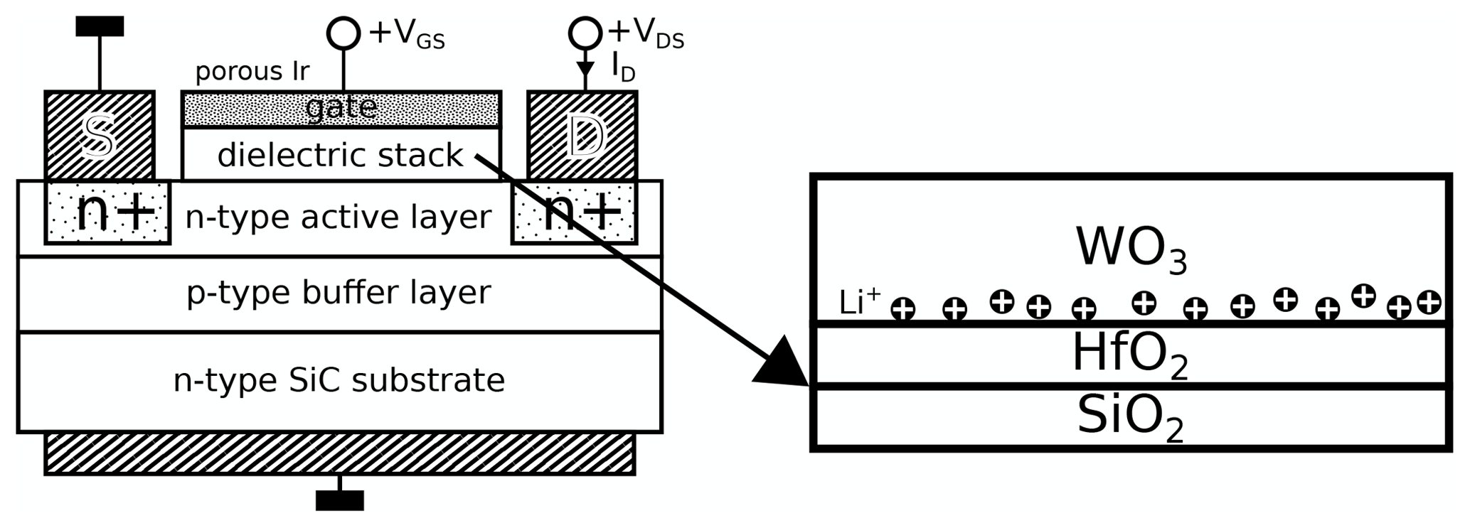
Figure 1Schematic of the used FET structure adapted from Andersson et al. (2013) highlighting the dielectric stack and the polarization effect with a positive VGS. The schematics are not to scale.
The as-deposited, both doped and undoped, sensor chips of approximately 2×2 mm2 in size, each containing two FET structures, were attached to a heater substrate (Heraeus Sensor-Nite GmbH, Kleinostheim, Germany) for the electrical and gas characterizations, along with a Pt100 temperature sensor (Heraeus Sensor-Nite GmbH), using a high-temperature, non-conducting ceramic adhesive (AREMCO 571). The heater substrate was then mounted on a 16-pin TO8 header and electrically contacted together with the Pt100 temperature sensor by spot welding to pins on the TO8 header. The SiC-FET device was electrically connected to the pins of the TO8 header by gold wire bonding. Before the first measurement, each sensor was burned in using the internal heater for at least 24 h at 400 ∘C.
2.2 Hardware and electronics
The electronic measurement equipment for setting the operation parameters (temperature and gate bias voltage) and read-out of the sensor signals was developed by 3S GmbH, Saarbrücken, Germany. It can adjust the sensor temperature between 70 and 400 ∘C with a resolution of 1 ∘C and controls the drain-source (VDS), gate-source (VGS), and substrate-source (or bulk) (VBS) voltages. The drain current ID was measured as a sensor signal within the range from 0 to 500 µA at a constant VDS of +4 V. During the measurement, the sensors were kept at 300 ∘C.
A gas mixing system using dynamic dilution was utilized to expose the sensors to defined gas concentrations similar to the system described in Helwig et al. (2014). A commercial gas cylinder with 500 ppm ammonia gas was diluted into a carrier gas stream of dry zero air. The total flow over the sensor was kept at 100 mL min−1.
3.1 Morphological and structural characterization
The average roughness of the WO3 layer, calculated as the root mean square deviation (RMSD) of a 1×1 µm2 AFM micrograph, was 3 nm, indicating a very flat layer. The grain size of approximately 24 nm was determined from an XRD spectrum of the columnar layer. Further details about how these results have been achieved as well as more information about the following Raman measurements can be found in the Supplement.
The heat treatment has a strong influence on the layer morphology and distribution and orientation of crystalline phases. In the Raman spectra (Fig. 2), the change from amorphous (blue, as-deposited) to more oriented (black, in situ annealed) WO3 can be seen. The ε peaks at Raman shifts of 268 and 425 cm−1 as well as the γ peaks at 71 and 134 cm−1 are clearly visible, whereas the ε peak at 372 cm−1 and the γ peak at 187 cm−1 are not pronounced much (Cazzanelli et al., 1999). As most of the ε and γ peaks are very close to each other and the peaks are mostly broad, it is difficult to determine which orientation is dominating. The peak at a Raman shift of 521 cm−1 obviously belongs to the silicon substrate and exceeds the intensity measured for tungsten oxide by 1 order of magnitude. Above a shift of 600 cm−1, W–O stretching from the amorphous phase is observed for the as-deposited (RT) sample as a wide hump (Baserga et al., 2007). It has been stated in the literature that the ε phase has a Raman mode at 678 cm−1, while the γ phase has a distinct peak at 717 cm−1 (Cazzanelli et al., 1999; Righettoni et al., 2010). Thus, the Raman measurement indicates that the in situ annealed sample contains more of the ε phase.
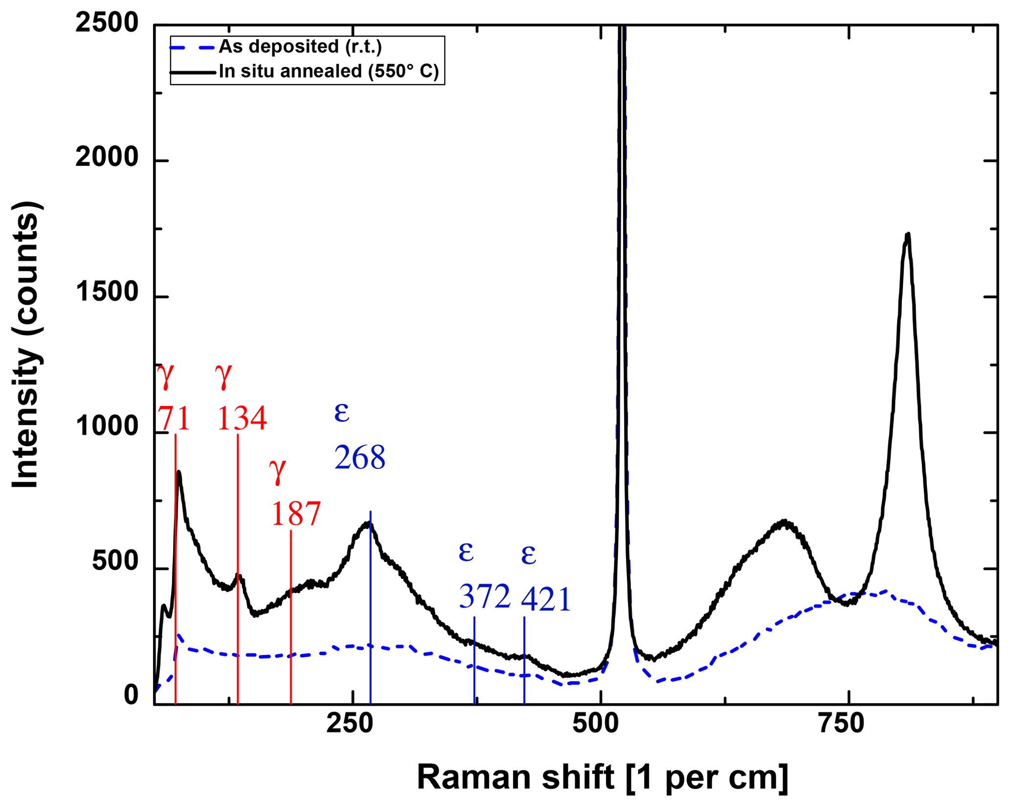
Figure 2Raman spectra for undoped WO3 layers deposited at room temperature (blue, dashed) and at 550 ∘C (black, solid).
3.2 Electrical characterization
The drain current ID was measured in zero air at different gate-source voltages VGS (Fig. 3a). The IV curve shows, for both doped and undoped devices, the expected behaviour of a normally on, n-type FET, i.e. significant current flow at VGS=0 V and an increase in current with the gate bias. When the gate bias is changed abruptly (Fig. 3b), the undoped sensor shows the expected behaviour of an n-type FET; i.e. the current increases, almost instantaneously, with the gate bias. The same effect is observed for the doped sensor (solid blue line) with an additional overshoot, marked with a circle, right after every gate bias step, followed by a relaxation effect. This is exemplarily shown for a switch from 0 to ±0.5 V. Another measurement with voltages up to ±2 V is shown in the Supplement (Fig. S3). One possible explanation for this behaviour can be the following: a positive gate bias pushes the lithium cations down, i.e. away from the surface, so that more free electrons are available close to the surface. With the abundance of electrons, the surface coverage with oxygen anions increases over time (Sauerwald et al., 2007), partly compensating for the positive gate bias and lowering the measured current until the oxygen surface coverage has reached its new equilibrium. The opposite happens for negative gate biases: lithium cations partly bind electrons close to the surface, resulting in a decreasing oxygen surface coverage and an increasing current. Alternatively, or additionally, this observation could also be explained by an electrochemical variation of the surface reactions similar to the EPOC effect, which creates an effective double layer of Li+ ions hindering oxygen adsorption to the sensor surface when a negative bias is applied (Katsaounis, 2010).
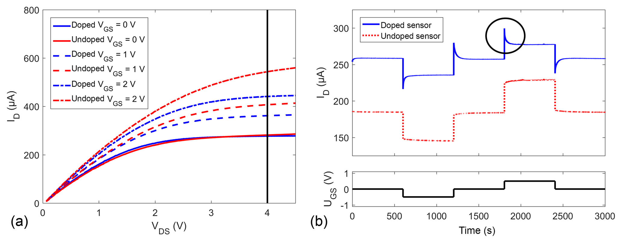
Figure 3(a) IV curves at different gate biases for doped and undoped sensors with indication of the measurement set point of VDS=4 V and (b) drain current ID at different gate biases for doped and undoped samples annealed in situ with a circle exemplarily highlighting one overshoot for the doped sensor. The different gate potentials −0.5, 0, and +0.5 V are shown in the lower subplot. The measurements in (a) and (b) were done some time apart, so that the slight baseline shift can be explained by sensor drift.
The relaxation after the initial peak was fitted over 300 s to gain information about the time constant τ using the following exponential equation:
The fit parameters are the terminal current, I0, the amplitude, A, and the time constant, τ. The parameter t0 is the starting point of the fit in time. The relaxation exhibits time constants between 20 and 30 s. The high mobility of Li+ in WO3 (Niklasson and Granqvist, 2007) disqualifies ionic movement as the sole explanation for the observed relaxation – the time constant estimated from mobility and the electric field is already at room temperature one order of magnitude below the measured effect, supporting the slower oxygen surface coverage as an explanation. This would, at the same time, explain the lower transconductance, i.e. change in ID with UGS, observed in Fig. 3.
3.3 Gas response
The FET sensor samples were exposed to two different ammonia concentrations (10 and 100 ppm) in dry air at a sensor temperature of 300 ∘C. Ammonia was selected as a model gas to investigate the influence of the gate bias: it is one of the most studied gases for SiC-FETs in particular and was shown to interact well with WO3 as a sensing material (Wang et al., 2006). Each concentration was offered for 30 min with 60 min of zero air after each gas exposure to allow relaxation to the baseline. Figure 4 shows the different responses ΔID, i.e. the difference between the measured drain current with and without gas exposure, of the doped (a) and undoped (b) sensors for gate biases of 0, +1, and +2 V. The quantization error of the response is ±60 nA. Both sensors exhibit a clearly concentration-dependent response. The higher response of the undoped sensor at 0 and 1 V is, most likely, due to variations in the manufacturing process of the transistor structure. It has been reported that the threshold voltage of these FET devices may vary within the same batch, influencing the sensitivity baseline (Andersson et al., 2013). The undoped sensor's response is independent of the applied gate bias and is approximately 12 and 20 µA for 10 and 100 ppm NH3, respectively. In contrast, the doped sensor's response is strongly influenced by the gate bias. While the response is 3 and 6 µA at 0 V, it increases to 9 and 28 µA, at 2 V for 10 and 100 ppm, respectively.
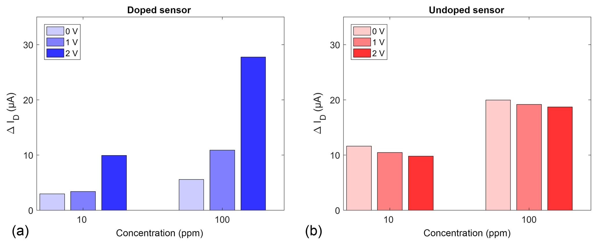
Figure 4Sensor response at different gate biases of 0, 1, and 2 V for a doped (a) and an undoped (b) sensor at 10 and 100 ppm NH3.
The undoped sensor shows the expected logarithmic response dependence of a FET (Eriksson and Ekedahl, 1998), which can be seen from the ratio of the response of 1:2 between 10 and 100 ppm. This ratio stays the same for all applied gate biases and also for the doped sensor at 0 V. For the latter, it increases, however, up to 1:3 at +2 V. The sensitivity, estimated from the quotient of response difference and concentration difference, follows the same pattern: it stays at a constant 96±3 nA per ppm for the undoped device, but increases from 29 to 198 nA per ppm for the doped device at 0 and +2 V, respectively. These findings fit the explanation given in Sect. 3.2, i.e. a changing oxygen surface coverage. Fogelberg et al. (1987) have shown that oxygen coverage promotes ammonia dissociation, at least for palladium, which, like iridium, belongs to the platinum metals. For metal-oxide sensors, a high oxygen coverage, achieved by quick temperature changes, results in a highly sensitive state (Baur et al., 2015). With the addition of Li+-doped WO3 in the FET's dielectric stack, a similar state could then be reached by quick gate bias changes, which give the additional benefit of much easier control compared to temperature. The increase in response at a positive gate bias is consistent with the expected increased catalytic activity due to the removal of lithium cations from the catalytic sites (Katsaounis, 2010). However, lithium-doped tungsten oxide as a mixed conductor has additional effects compared to classical EPOC catalysts, which are pure ionic conductors. The most important difference is that the electron density in tungsten oxide is increased by lithium doping as well (Niklasson and Granqvist, 2007). In the surface state trapping model this leads to an increase in surface oxygen (Ding et al., 2001). This increase in oxygen coverage is presumably the reason for the higher sensitivity of the doped sensors.
A second pair of sensors from a second production batch was tested with similar and different concentrations and gate biases to verify the doping effect. The results are shown in Figs. S3 and S4 in the Supplement.
Pulsed laser deposition parameters have been successfully optimized to deposit dense WO3 films on top of SiC-FET devices. The distribution and orientation of crystalline phases can be adjusted by heat treatment during the deposition. In situ annealing leads to a more ordered and stable structure with a comparably high amount of the ε phase. This ordered layer was deposited as the top-most layer of the dielectric stack of a SiC-FET and the effect of Li doping of this layer on the sensor response was studied. The sensor with a doped layer exhibits strong relaxation processes for GBCO with time constants of the order of 10 s. This effect, presumably caused by electrochemical polarization, can be utilized to boost the effect of GBCO as demonstrated by ammonia tests. While the response for the undoped layer is almost independent of the gate bias, it increases for the doped layer up to 5-fold between 0 and +2 V gate bias. Additionally, the doped layer shows increased sensitivity at +2 V gate bias. We could demonstrate that ionic polarization has a large impact on the sensor characteristics and that it can be utilized to boost the sensor's sensitivity. Furthermore, the ionic polarization increases the impact of gate bias variation on the sensor signal. Therefore, we expect that this method can result in enhanced performance of GBCO and, consequently, selectivity.
Research data are available upon request to the authors.
The supplement related to this article is available online at: https://doi.org/10.5194/jsss-8-261-2019-supplement.
MR, MB, TS, and MA planned the measurements. JH carried out the Raman measurements and evaluation and supervised the PLD process. MR carried out all other measurements and did most of the evaluation. JP performed the XRD data evaluation. MR, MB, and TS prepared a concept of the manuscript. MR wrote the manuscript. MB, TS, JL, MA, and AS contributed with substantial revisions.
The authors declare that they have no conflict of interest.
The authors want to thank the technical support of the Center of Microscopy and Nanotechnology of the University of Oulu. We acknowledge the support by the European Cooperation in Science and Technology (within COST Action TD1105-EuNetAir) and by the Deutsche Forschungsgemeinschaft (DFG, German Research Foundation) within the Open Access Publishing funding programme.
We have received support for scientific exchange from the European Cooperation in Science and Technology and support for Open Access Publishing from the Deutsche Forschungsgemeinschaft and Saarland University.
This paper was edited by Albert Romano-Rodriguez and reviewed by two anonymous referees.
Andersson, M., Pearce, R., and Lloyd Spetz, A.: New generation SiC based field effect transistor gas sensors, Sensors Actuators B Chem., 179, 95–106, https://doi.org/10.1016/j.snb.2012.12.059, 2013.
Baserga, A., Russo, V., Di Fonzo, F., Bailini, A., Cattaneo, D., Casari, C. S., Li Bassi, A., and Bottani, C. E.: Nanostructured tungsten oxide with controlled properties: Synthesis and Raman characterization, Thin Solid Films, 515, 6465–6469, https://doi.org/10.1016/j.tsf.2006.11.067, 2007.
Bastuck, M., Bur, C., Lloyd Spetz, A., Andersson, M., and Schütze, A.: Gas identification based on bias induced hysteresis of a gas-sensitive SiC field effect transistor, J. Sens. Sens. Syst., 3, 9–19, https://doi.org/10.5194/jsss-3-9-2014, 2014.
Baur, T., Schütze, A., and Sauerwald, T.: Optimierung des temperaturzyklischen Betriebs von Halbleitergassensoren, Tech. Mess., 82, 187–195, https://doi.org/10.1515/teme-2014-0007, 2015.
Berggren, L.: Optical Absorption and Electrical Conductivity in Lithium Intercalated Amorphous Tungsten Oxide Films, Uppsala University, 2004.
Berggren, L., Ederth, J., and Niklasson, G. A.: Electrical conductivity as a function of temperature in amorphous lithium tungsten oxide, Sol. Energy Mater. Sol. Cells, 84, 329–336, https://doi.org/10.1016/j.solmat.2004.02.049, 2004.
Bur, C.: Selectivity Enhancement of Gas Sensitive Field Effect Transistors by Dynamic Operation, Universität des Saarlandes, Saarbrücken, 2015.
Bur, C., Bastuck, M., Lloyd Spetz, A., Andersson, M., and Schütze, A.: Selectivity enhancement of SiC-FET gas sensors by combining temperature and gate bias cycled operation using multivariate statistics, Sensors Actuators B Chem., 193, 931–940, https://doi.org/10.1016/j.snb.2013.12.030, 2014.
Cazzanelli, E., Vinegoni, C., Mariotto, G., Kuzmin, A., and Purans, J.: Low-Temperature Polymorphism in Tungsten Trioxide Powders and Its Dependence on Mechanical Treatments, J. Solid State Chem., 143, 24–32, https://doi.org/10.1006/jssc.1998.8061, 1999.
Ding, J., McAvoy, T. J., Cavicchi, R. E., and Semancik, S.: Surface state trapping models for SnO2-based microhotplate sensors, Sensors Actuators, B Chem., 77, 597–613, https://doi.org/10.1016/S0925-4005(01)00765-1, 2001.
Eason, R. (Ed.): Pulsed Laser Deposition of Thin Films: Applications-Led Growth of Functional Materials, John Wiley & Sons, New Jersey, 2007.
Eriksson, M. and Ekedahl, L.-G.: Hydrogen adsorption states at the Pd/SiO2 interface and simulation of the response of a Pd metal–oxide–semiconductor hydrogen sensor, J. Appl. Phys., 83, 3947, https://doi.org/10.1063/1.367150, 1998.
Fogelberg, J., Lundstrom, I., and Petersson, L. G.: Ammonia dissociation on oxygen covered palladium studied with a hydrogen sensitive pd-mos device, Phys. Scr., 35, 702–705, https://doi.org/10.1088/0031-8949/35/5/017, 1987.
Helwig, N., Schüler, M., Bur, C., Schütze, A., and Sauerwald, T.: Gas mixing apparatus for automated gas sensor characterization, Meas. Sci. Technol., 25, 055903, https://doi.org/10.1088/0957-0233/25/5/055903, 2014.
Katsaounis, A.: Recent developments and trends in the electrochemical promotion of catalysis (EPOC), J. Appl. Electrochem., 40, 885–902, https://doi.org/10.1007/s10800-009-9938-7, 2010.
Kim, Y. S., Ha, S. C., Kim, K., Yang, H., Choi, S. Y., Kim, Y. T., Park, J. T., Lee, C. H., Choi, J., Paek, J., and Lee, K.: Room-temperature semiconductor gas sensor based on nonstoichiometric tungsten oxide nanorod film, Appl. Phys. Lett., 86, 1–3, https://doi.org/10.1063/1.1929872, 2005.
Kiselev, I., Sommer, M., and Sysoev, V. V.: Electric field-induced rearrangement of charged species in metal oxide devices with resistive change: thermodynamic limitations, Eur. Phys. J. B, 82, 7–12, https://doi.org/10.1140/epjb/e2011-20176-0, 2011.
Lee, A. P. and Reedy, B. J.: Temperature modulation in semiconductor gas sensing, Sensors Actuators B Chem., 60, 35–42, https://doi.org/10.1016/S0925-4005(99)00241-5, 1999.
Leidinger, M., Sauerwald, T., Reimringer, W., Ventura, G., and Schütze, A.: Selective detection of hazardous VOCs for indoor air quality applications using a virtual gas sensor array, J. Sens. Sens. Syst., 3, 253–263, https://doi.org/10.5194/jsss-3-253-2014, 2014.
Leidinger, M., Huotari, J., Sauerwald, T., Lappalainen, J., and Schütze, A.: Nanostructured WO3 Semiconductor Gas Sensor for Selective Detection of Naphthalene, in: AMA Conferences 2015 – SENSOR 2015 and IRS2 2015, 723–728, 2015.
Leidinger, M., Huotari, J., Sauerwald, T., Lappalainen, J., and Schütze, A.: Selective detection of naphthalene with nanostructured WO3 gas sensors prepared by pulsed laser deposition, J. Sens. Sens. Syst., 5, 147–156, https://doi.org/10.5194/jsss-5-147-2016, 2016.
Liess, M.: Electric-field-induced migration of chemisorbed gas molecules on a sensitive film – a new chemical sensor, Thin Solid Films, 410, 183–187, https://doi.org/10.1016/S0040-6090(02)00209-2, 2002.
Llobet, E., Molas, G., Molinàs, P., Calderer, J., Vilanova, X., Brezmes, J., Sueiras, J. E., and Correig, X.: Fabrication of Highly Selective Tungsten Oxide Ammonia Sensors, J. Electrochem. Soc., 147, 776, https://doi.org/10.1149/1.1393270, 2000.
Lloyd Spetz, A. and Andersson, M.: Technology and Application Opportunities for SiC-FET Gas Sensors, in: Solid State Gas Sensors – Industrial Application, edited by: Fleischer, M. and Lehmann, M., 189–214, Springer, Berlin, 2012.
Morimune, T., Yamaguchi, H., and Yasukawa, Y.: Study of catalytic reduction of NO(x) in exhaust gas from a diesel engine, Exp. Therm. Fluid Sci., 18, 220–230, https://doi.org/10.1016/S0894-1777(98)10025-0, 1998.
Nakagomi, S., Fukumura, A., Kokubun, Y., Savage, S., Wingbrant, H., Andersson, M., Lundström, I., Löfdahl, M., and Lloyd Spetz, A.: Influence of gate bias of MISiC-FET gas sensor device on the sensing properties, Sensors Actuators B Chem., 108, 501–507, https://doi.org/10.1016/j.snb.2004.11.057, 2005.
Niklasson, G. A. and Granqvist, C. G.: Electrochromics for smart windows: thin films of tungsten oxide and nickel oxide, and devices based on these, J. Mater. Chem., 17, 127–156, https://doi.org/10.1039/b612174h, 2007.
Penza, M., Tagliente, M. A., Mirenghi, L., Gerardi, C., Martucci, C., and Cassano, G.: Tungsten trioxide (WO3) sputtered thin films for a NOx gas sensor, Sensors Actuators B Chem., 50, 9–18, https://doi.org/10.1016/S0925-4005(98)00149-X, 1998.
Pohle, R., Von Sicard, O., Fleischer, M., Frerichs, H. P., Wilbertz, C., and Freund, I.: Gate pulsed readout of floating gate FET gas sensors, Procedia Eng., 5, 13–16, https://doi.org/10.1016/j.proeng.2010.09.036, 2010.
Puglisi, D., Eriksson, J., Bastuck, M., Bur, C., Huotari, J., and Andersson, M.: Exploring the gas sensing performance of catalytic metals and metal oxides on 4H-SiC field effect transistors, in: International Conference on Silicon Carbide and Related Materials, Giardini Naxos, 2015.
Righettoni, M., Tricoli, A., and Pratsinis, S. E.: Thermally stable, silica-doped ε-WO3 for sensing of acetone in the human breath, Chem. Mater., 22, 3152–3157, https://doi.org/10.1021/cm1001576, 2010.
Sauerwald, T., Skiera, D., and Kohl, D.: Field induced polarisation and relaxation of tungsten oxide thick films, Thin Solid Films, 490, 86–93, https://doi.org/10.1016/j.tsf.2005.04.009, 2005.
Sauerwald, T., Skiera, D., and Kohl, D.: Selectivity enhancement of gas sensors using non-equilibrium polarisation effects in metal oxide films, Appl. Phys. A Mater. Sci. Process., 87, 525–529, https://doi.org/10.1007/s00339-007-3980-2, 2007.
Shaver, P. J.: Activated Tungsten Oxide Gas Detectors, Appl. Phys. Lett., 11, 255–257, https://doi.org/10.1063/1.1755123, 1967.
Solis, J. L., Saukko, S., Kish, L., Granqvist, C. G., and Lantto, V.: Semiconductor gas sensors based on nanostructured tungsten oxide, Thin Solid Films, 391, 255–260, https://doi.org/10.1016/S0040-6090(01)00991-9, 2001.
Strømme Mattsson, M.: Li insertion into WO3: Introduction of a new electrochemical analysis method and comparison with impedance spectroscopy and the galvanostatic intermittent titration technique, Solid State Ionics, 131, 261–273, https://doi.org/10.1016/S0167-2738(00)00674-3, 2000.
Varpula, A., Novikov, S., Haarahiltunen, A. and Kuivalainen, P.: Transient characterization techniques for resistive metal-oxide gas sensors, Sensors Actuators B Chem., 159, 12–26, https://doi.org/10.1016/j.snb.2011.05.059, 2011.
Wang, G., Ji, Y., Huang, X., Yang, X., Gouma, P. I., and Dudley, M.: Fabrication and characterization of polycrystalline WO3 nanofibers and their application for ammonia sensing, J. Phys. Chem. B, 110, 23777–23782, https://doi.org/10.1021/jp0635819, 2006.
Wang, L., Teleki, A., Pratsinis, S. E., and Gouma, P. I.: Ferroelectric WO3 nanoparticles for acetone selective detection, Chem. Mater., 20, 4794–4796, https://doi.org/10.1021/cm800761e, 2008.
Willmott, P. R. and Huber, J. R.: Pulsed laser vaporization and deposition, Rev. Mod. Phys., 72 315–328, https://doi.org/10.1103/RevModPhys.72.315, 2000.