the Creative Commons Attribution 4.0 License.
the Creative Commons Attribution 4.0 License.
 | 16 Jul 2020
Analysis of photoelastic properties of monocrystalline silicon
Markus Stoehr
Gerald Gerlach
Thomas Härtling
Stephan Schoenfelder
Photoelasticity is considered a useful measurement tool for the non-destructive and contactless determination of mechanical stresses or strains in the production of silicon wafers. It describes a change in the indices of refraction of a material when the material is mechanically loaded. As silicon has a diamond lattice structure, the stress-dependent change in the refractive indices varies with the loading direction. In this work, an anisotropic stress-optic law is derived, and the corresponding stress-optical parameters are measured using a Brazilian disc test. The parameters were determined to be MPa−1 and MPa−1. The results of this work are compared to previous works found in the literature, and the deviations are discussed.
- Article
(5657 KB) - Full-text XML
- BibTeX
- EndNote


The photoelastic measurement of mechanical stresses is based on the birefringence caused by mechanical stresses (or strains). Birefringence describes the ability of materials to split an incident electromagnetic wave into two refracted waves instead of one (Zinth and Zinth, 2009). These two refracted waves of light show different coefficients of refraction and different states of polarization depending on mechanical stresses. This change can be measured by a polariscope, and mechanical stresses can be deduced from the measured change (Wolf, 1961; Ramesh, 2000).
Photoelasticity was first described by David Brewster in the early 19th century (Brewster, 1815, 1816), and the first analytical models to describe it were published some years later (Neumann, 1841; Pockels, 1889, 1906). In the early 20th century, the first industry applications for experimental stress measurements by means of photoelasticity can be found (Wolf, 1961). Photoelasticity was a key method to determine stresses by building models out of photoelastically active materials. This was extensively used until numerical methods, e.g. the finite element method, became more powerful and convenient for the evaluation of stresses (Ramesh, 2000). However, photoelasticity is still used as an in-line measurement method for glasses to directly measure mechanical stresses (Vivek and Ramesh, 2015). In the same manner, it could be applied to production processes for silicon wafers, as silicon is transparent with respect to infrared light. Some research, e.g. Lederhandler (1959), Brito et al. (2005), Ganapati et al. (2010), Jagailloux et al. (2016) and Herms et al. (2019), has been carried out in this field in recent years.
A mechanical stress applied to a material susceptible to stress-induced birefringence results in a change in the difference of the two polarization states and, hence, a change in the indices of refraction n1 and n2:
This change can be measured using a polariscope by measuring the phase difference δ between the two refracted light waves that increases with material thickness t:
For mechanically and photoelastically isotropic materials, the phase difference δ is proportional to the difference in the first and second principal stresses (σI, σII) for plane stress conditions:
The stress-optical coefficient C generally depends on the material and wavelength. It relates the difference between the principal stresses σI and σII to the phase difference δ.
Silicon has an inherent mechanical and photoelastic anisotropy because of its lattice structure. Therefore, a corresponding model is required to determine the photoelastic properties of silicon. For mechanically and photoelastically anisotropic materials, Eq. (3) does not hold true. Silicon's lattice structure leads to a direction-dependent behaviour. In the literature, there are several different models that aim to describe the photoelastic properties of silicon. Some studies explicitly state the model used (Liang et al., 1992; He et al., 2004; Zheng and Danyluk, 2002), whereas others only include a brief description of their approach (Giardini, 1958; Ajmera et al., 1988; Krüger et al., 2016). However, those that explicitly state their derived model lead to different analytical expressions, even when based on the same approach, as can be seen in Fig. 1.
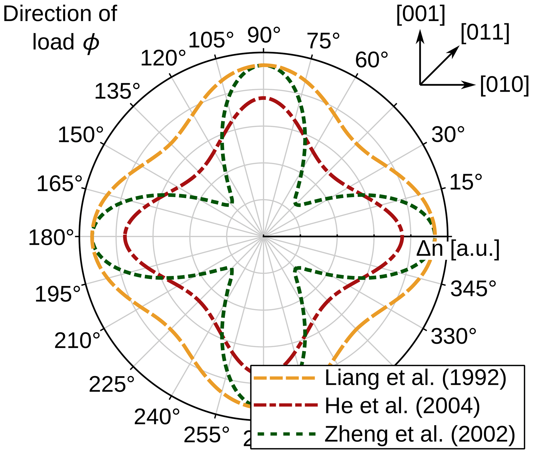
Figure 1Comparison of different reported models for photoelasticity in silicon from the literature expressed as the difference Δn between the coefficients of refraction (the orientations of differently defined coordinate systems have been aligned).
Therefore, in this work, photoelasticity in silicon is revisited and a new model based on the same phenomenological approach for birefringence and photoelasticity as that in Neumann (1841) and Pockels (1889, 1906) is derived to address the disagreement among the different models in the literature. Stress-optical parameters are determined by measurement using a polariscope and a (100)-silicon wafer in a Brazilian disc test. Results from this work are then compared to works from the literature, and the deviations are discussed.
Indices of refraction due to the birefringence of an unstressed material can be described using Maxwell's equations (Hecht, 2018; Zinth and Zinth, 2009). However, this approach leads to impractically long terms. In order to simplify this, an analogy is used that consists of an ellipsoid which expresses the material properties. In the literature, this ellipsoid is commonly called an index ellipsoid or an indicatrix. It is based on an imaginary light ray falling into the centre of the indicatrix. Perpendicular to this ray, a plane is constructed. The intersection of the plane and the indicatrix results in an ellipse. The lengths of the two half-axes of the ellipse correspond to the two indices of refraction. This is shown in Fig. 2.
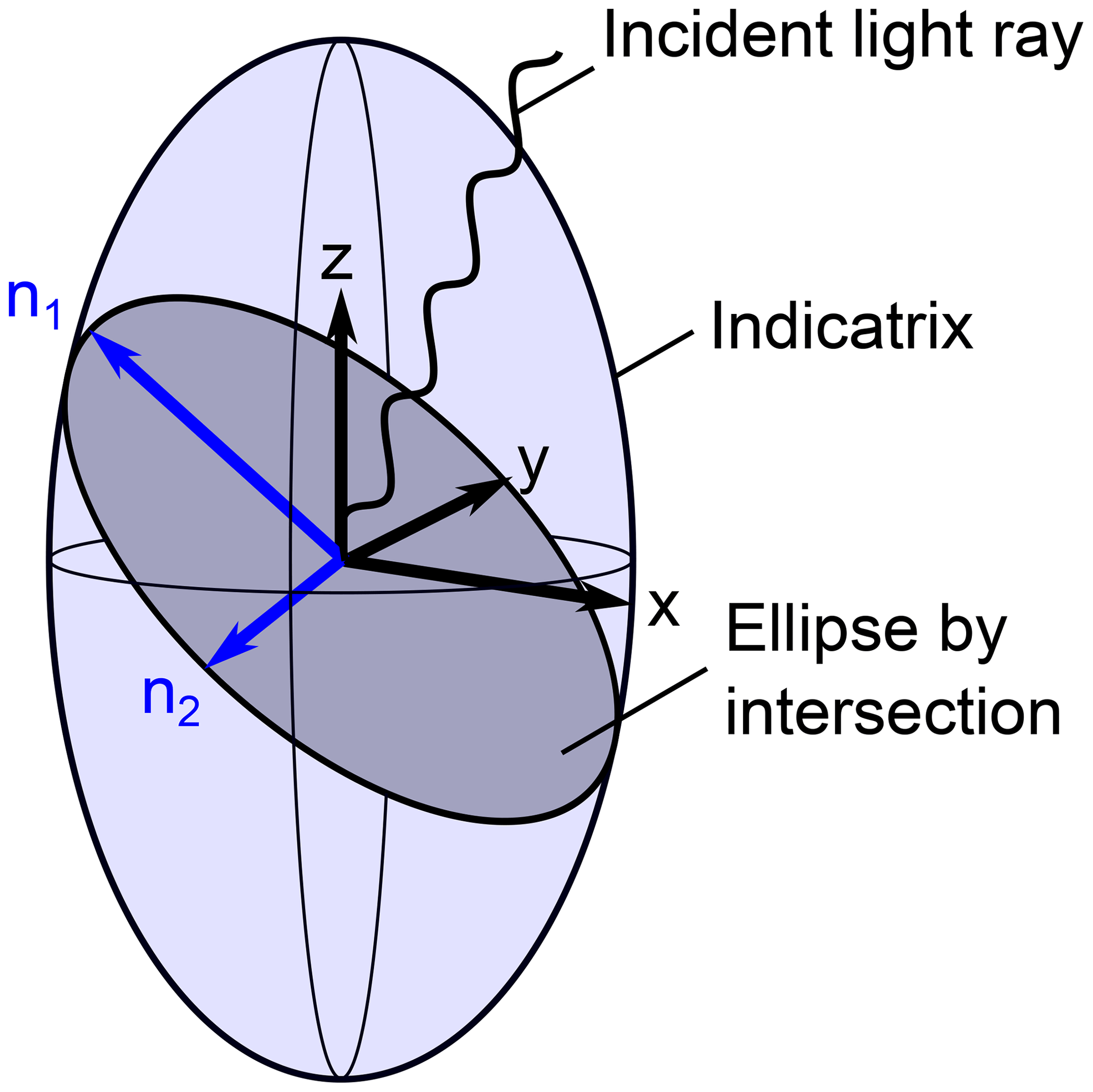
Figure 2Indicatrix as an analogy to describe two indices of refraction for a certain direction of incident light in a birefringent material.
The indicatrix is a quadratic surface that generally has six independent parameters:
in which Bij is a 3×3 symmetric second-order tensor that is material-dependent. It is called the impermeability tensor. Vector xi represents a Cartesian coordinate system which is defined in this work so that x1→x, x2→y and x3→z. Using the Einstein summation convention, Eq. (4) is expanded as follows:
By rotating the indicatrix to align with the (x, y, z)-coordinate system used, it can be expressed using just three independent values:
Here, BI, BII and BIII are principal values of Bij. By definition, the indicatrix can also be expressed as the reciprocal of the squared indices of refraction (nI, nII, nIII):
or, in a more general form, as
The phenomenological approach by Neumann (1841) and Pockels (1889, 1906) to describe photoelasticity in stressed materials links the change in impermeability ΔBij to the mechanical stress tensor σij and the mechanical strain tensor εij, respectively, using a fourth-order tensor. In terms of the analogy used, this means that mechanical stresses or strains deform the indicatrix by changing the impermeability matrix Bij by ΔBij:
Here, πijkl and pijkl are the stress-optical and strain-optical tensors, respectively. Both can be expressed by one another considering Hooke’s law for linear elasticity (Narasimhamurty, 1981). Therefore, in this work, only the stress-optical relationship is considered.
The change in impermeability is expressed as the difference between impermeability matrices Bij and in a stressed and unstressed state. Using Eq. (8), they can be expressed by the refraction indices nij and :
By converting them to a common denominator, this can be rewritten as follows:
The change in impermeability is assumed to be small compared with the unstressed impermeability, meaning that . Thus, two simplifications can be made:
With the above-mentioned simplifications, Eq. (11) can be expressed as follows:
This links a change in the indices of refraction to the change in impermeability ΔBij and, therefore, to mechanical stresses using Eq. (9). In the following, the approximation sign is omitted, although it is still an approximation that is only valid for small changes in impermeability. Rearranging Eq. (13) yields the following:
For an indicatrix whose half-axes are aligned to the coordinate system, this leads to a set of three equations:
With respect to Eq. (9), the change in the indices of refraction can be calculated for stress state σij using stress-optical tensor πijkl. Because the impermeability and the stress tensor are both symmetric second-order tensors, the stress-optical tensor πijkl also has to show certain symmetries (Narasimhamurty, 1981). This allows it to be written as a 6×6 matrix in Voigt notation. In this form, indices ij and kl of the tensor πijkl are reduced to 11→1, 22→2, 33→3, 23→4, 13→5 and 12→6. In the following, Voigt notation will be indicated by (V).
Due to the diamond structure of monocrystalline silicon, there are only three independent parameters of the stress-optical tensor (Narasimhamurty, 1981):
Attention has to be paid to accounting for the appropriate coefficients while converting from tensor notation to Voigt notation (Narasimhamurty, 1981). Accordingly, the stress-optical parameters in Voigt notation are related to the stress-optical coefficients πijkl in tensor notation by the following equation:
In order to account for different crystalline orientations of silicon, a rotation matrix Rij is introduced. The rotated stress-optical tensor accounts for different orientations of the silicon lattice structure by applying a rotation matrix Rij to it as follows:
For simplicity, in the following only mechanical stresses in-plane with the (100) plane of silicon are discussed. The [100] direction is further assumed to be parallel to the z axis of the coordinate system. A situation in which these simplifications arise is represented by a (100)-silicon wafer, as shown in Fig. 3. In this case, rotation matrix Rij(ϕ) describes a clockwise rotation around the z axis by an angle ϕ, which is the angle between the [010] direction and the x axis:
As the (100)-silicon wafer is considered sufficiently thin, only plane stresses are evaluated:
Inserting rotation matrix Rij(ϕ) into Eq. (18) and applying both to Eq. (9) yields the change in the impermeability tensor ΔBij for a plane stress state:
If the incident light ray falling onto the indicatrix is parallel to the z axis of the chosen coordinate system, Eq. (15c) can be neglected. Therefore, the change in the indices of refraction can be expressed by subtracting Eq. (15b) from Eq. (15a). Further, the natural birefringence is comparably small against stress-induced birefringence, meaning that (Krüger et al., 2016), yielding the following:
To obtain the principal values ΔBI and ΔBII, a simple eigenvalue analysis on the impermeability tensor of Eq. (21) can be performed:
in which
Inserting the principal values of Eqs. (23a) and (23b) into Eq. (22) yields the stress-optical law for a {100}-silicon wafer:
or, in more detail,
From this equation it can be seen that there are only two material-dependent parameters, as the difference between (π11−π12) cannot be separated.
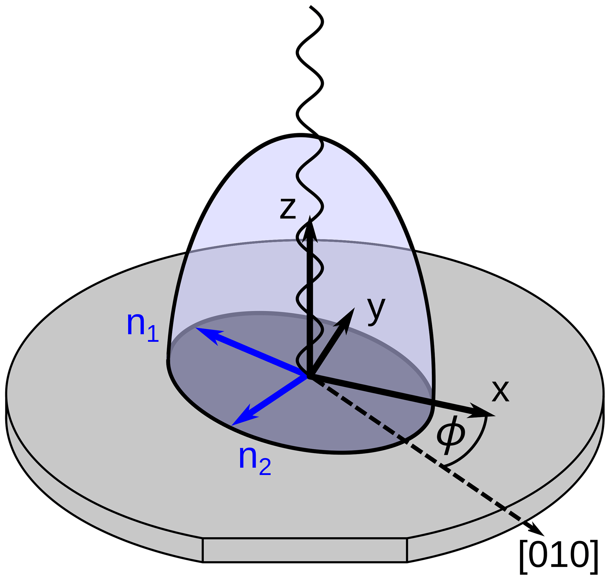
Figure 3Orientation of the indicatrix on a {100}-silicon wafer to describe the birefringence with reference to the global (x, y, z) coordinate system where the x–y plane is located on the [001] plane.
To describe a photoelastically isotropic material the stress-optical tensor πijkl of Eq. (16) is replaced with a stress-optical tensor for an isotropic material (Narasimhamurty, 1981):
Following the same derivation as for the anisotropic case, the stress-optical law reduces to the following equations:
which is equivalent to the law for isotropic photoelasticity as given in the literature (Wolf, 1961; Ramesh, 2000). The same can be achieved by replacing π44 with (π11−π12) in Eq. (26). The model derived is shown in Fig. 4 for three arbitrary parameter combinations, including one for isotropic parameters.
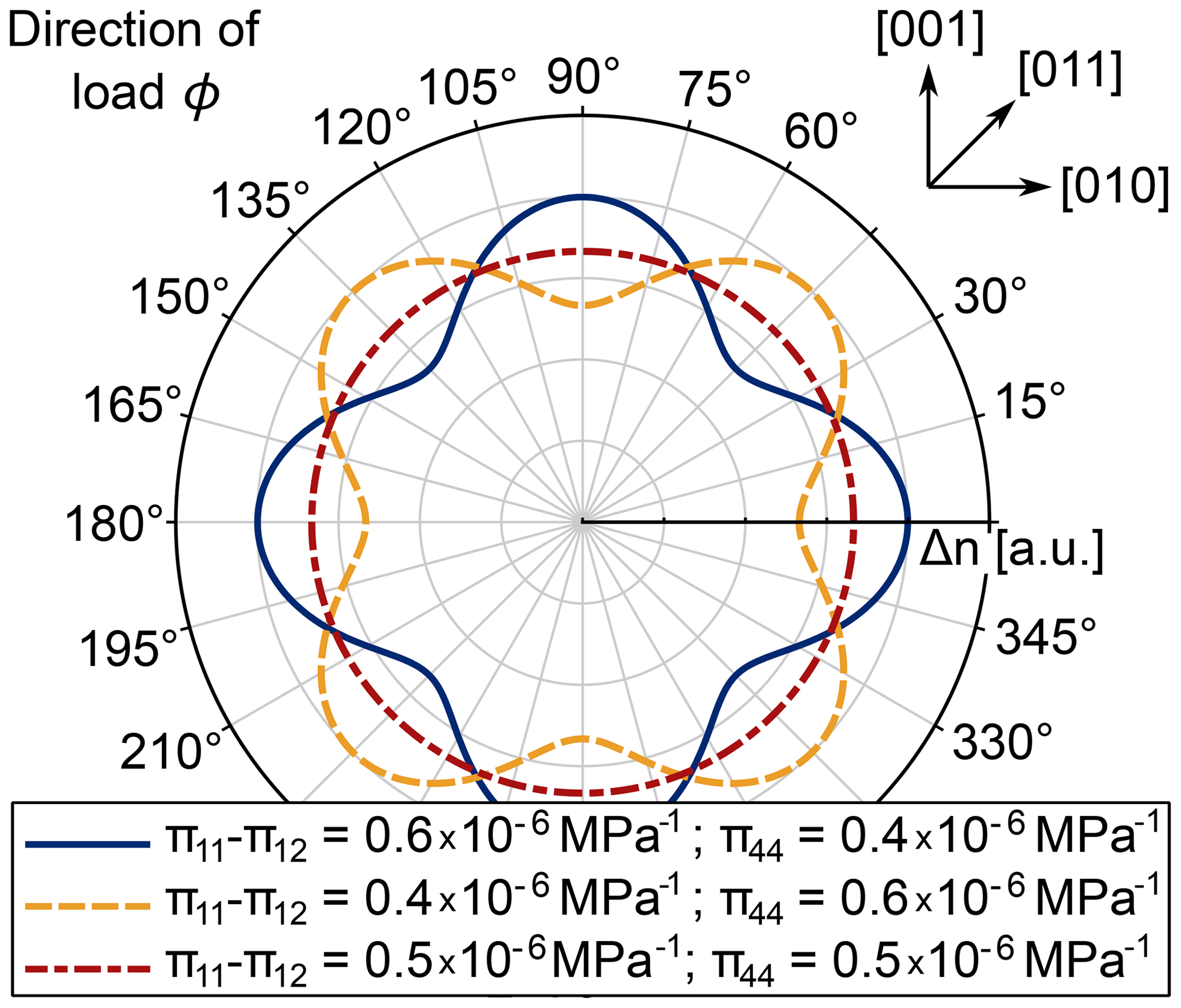
Figure 4The stress-optical model derived for a {100}-silicon wafer with three arbitrarily chosen parameter combinations.
In order to measure the coefficients of πijkl, a Brazilian disc test was used (as depicted in Fig. 5). The stress-induced retardation was measured using a grey field polariscope, as shown in Fig. 6. In parallel, mechanical stresses σ11, σ22 and σ12 were determined using the finite element method with Ansys Mechanical APDL. This allows for a full mapping of mechanical stresses onto the measured retardation values with consideration of the anisotropic mechanical response of a (100)-silicon wafer. Retardation values and stresses were correlated using Eq. (26) to determine the parameters (π11−π12) and π44.
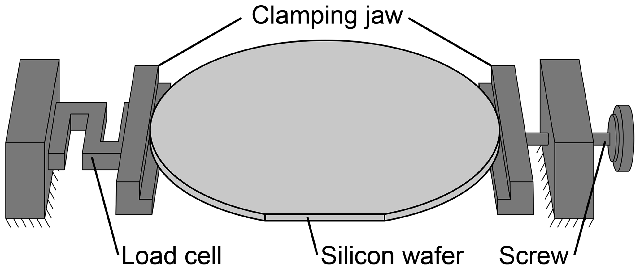
Figure 5Brazilian disc test for a load along the [011] direction used to determine stress-optical parameters for a (100)-silicon wafer.
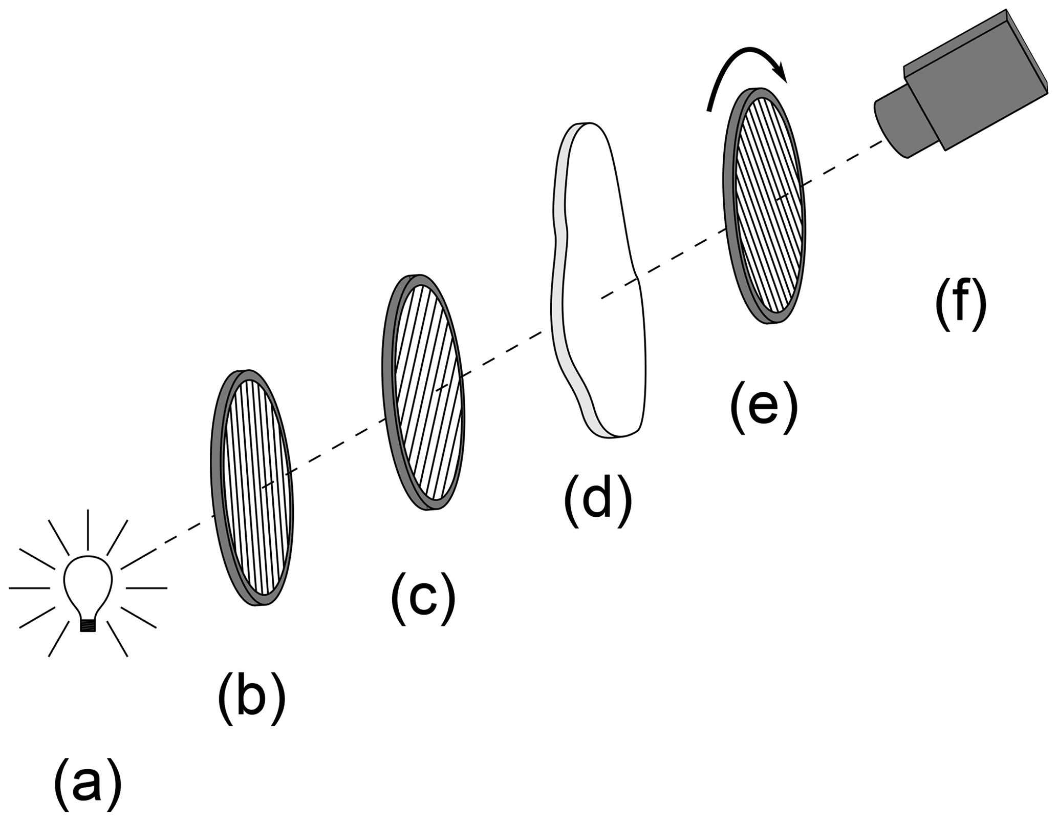
Figure 6Grey field polariscope (Horn et al., 2005) consisting of (a) a light source, (b) a linear polarizer, (c) a quarter wave plate, (d) a probe, (e) a rotating linear polarizer and (f) a camera.
The grey field polariscope uses circularly polarized light in the near-infrared spectral range. With this device, retardation values up to a quarter of the wavelength utilized can be measured without manual determination of fringe values. The measurement principle is described in detail elsewhere (Horn et al., 2005). Linked to the polariscope is a computer that calculates the retardation and the orientation of the optical axes from measured light intensities and saves both in ASCII format.
The Brazilian disc test consists of two diametrically placed clamping jaws that load the wafer on its thin sides. Force on the jaws is manually applied by a screw and is measured by a load cell. To mitigate high contact stresses, several layers of adhesive tape were placed in the contact areas of the jaws. This leads to a reduction in the applied force due to the relaxation of the tape material, which was taken into account by waiting for about 5 min before each measurement. For all measurements, the difference between start and end force was smaller than 0.1 N for an applied force of 10 N. This load is sufficient for a distinct measurable photoelastic signal without buckling the wafer. Buckling was observed to start at approx. 20 N.
The wafer was manually inserted between the clamping jaws. In total, 28 measurements were carried out for angles from −60 to 60∘ with respect to the [011]-wafer direction. Angles were varied in increments of approx. 2.5∘. The orientation of the wafer was measured graphically from video data from the polariscope as the angle between the clamping jaw edge and the wafer flat.
For the finite element simulation of the Brazilian disc test, 19 200 elements with a quadratic displacement function were used in a linear elastic simulation. For each measurement, the mechanical stresses were simulated considering the specific applied load and the wafer orientation.
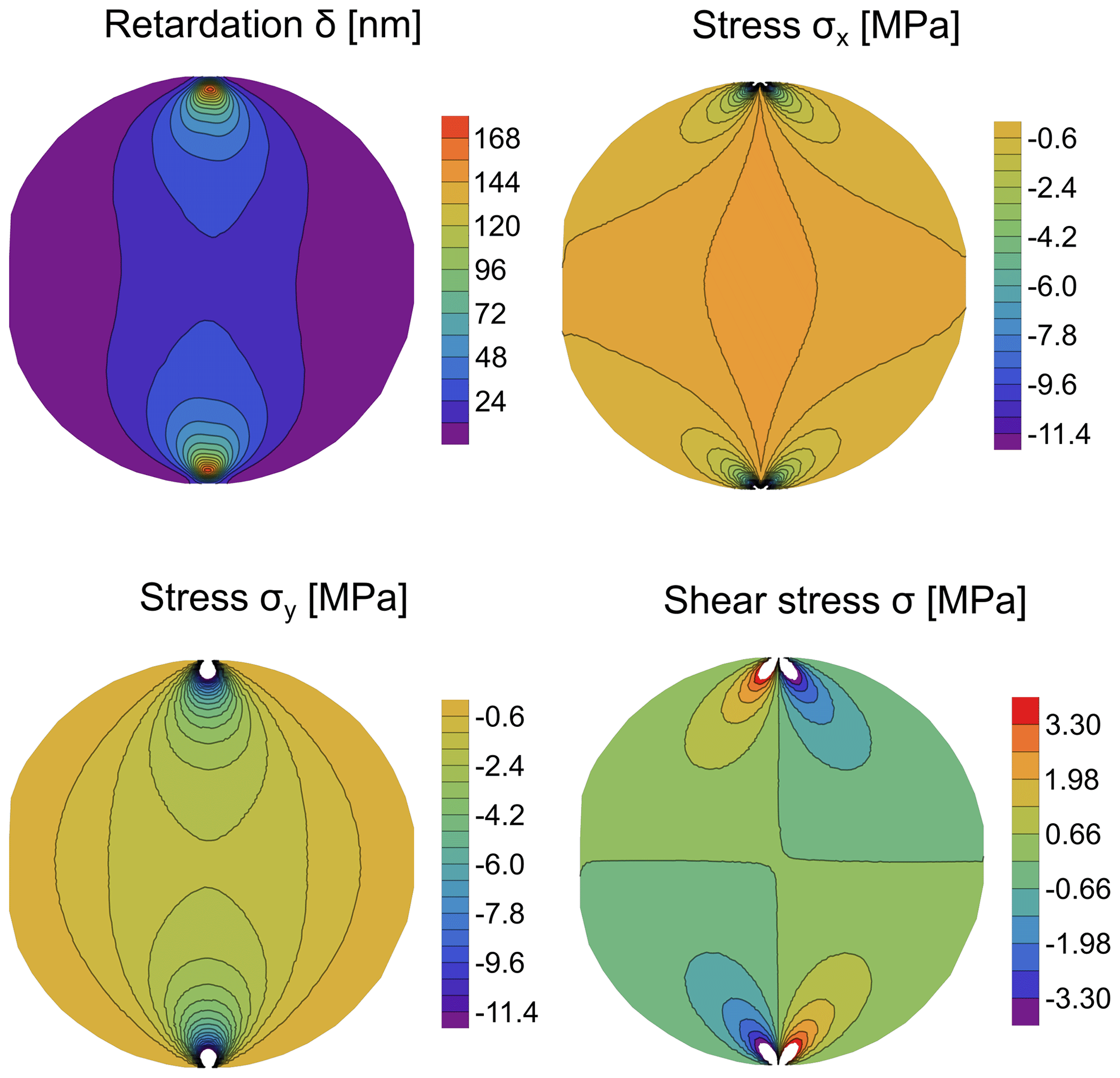
Figure 7Example of measured retardation δ values and simulated stresses σ11, σ22 and σ12 for a loading direction of ϕ=45∘ and a load of F=10 N.

Figure 8Stress-optical law for a {100}-silicon wafer with 95 % confidence level (blue band), and the angle-dependent stress-optical coefficients C(ϕ) with a 95 % confidence level (yellow). Stress-optical coefficients are displayed neglecting shear stresses.
Figure 7 shows the measured retardation values and the simulated stresses as an example of loading along the [011] direction of the wafer. From these, mechanical stresses and retardation measurements were taken to determine the stress-optical coefficients using a least-squares fit algorithm for Eq. (27). The stress-optical coefficients were determined to be MPa−1 and MPa−1. The fitted model of Eq. (27) shows a coefficient of determination (R2) of 0.81 for the angle-dependent stress-optical coefficients, and it is deemed to be a good fit. The levels of confidence were estimated by 10 repeated measurements for wafer orientations of 0 and 45∘. Confidence intervals for the measurement of wafer angles were assumed to be ±1∘ at a 95 % confidence level. To estimate the confidence level of the fitted parameters, a Monte Carlo simulation for the non-linear fit of Eq. (27) was carried out. In Fig. 8, retardation δ based on Eq. (27) is shown for a normalized wafer thickness t and a normalized stress difference (σI−σII) with measured stress-optical coefficients. Also, the angle-dependent isotropic coefficients C(ϕ) based on Eq. (3) for each measurement are plotted. Confidence intervals for the determined wafer orientations are smaller then the plotted dot in Fig. 8 and are therefore omitted.
In comparison to models given in the literature, the stress-optical law derived in this work shows a close resemblance in shape to the work of Liang et al. (1992) and He et al. (2004). This can be seen in Fig. 9 for a normalized stress difference and a normalized wafer thickness. The work by Zheng and Danyluk (2002) shows a higher degree of anisotropy then other models. Quantitatively, this work shows a stronger stress-optical effect then studies in the literature (Liang et al., 1992; Zheng and Danyluk, 2002; He et al., 2004). This is reflected by the determined stress-optical coefficients which are higher then previously reported values, as shown in Table 1.
Liang et al. (1992)He et al. (2004)Zheng and Danyluk (2002)Giardini (1958)Table 1Stress-optical coefficients for a (100) silicon from experiments in this study and from the literature.
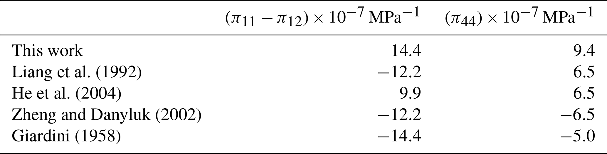
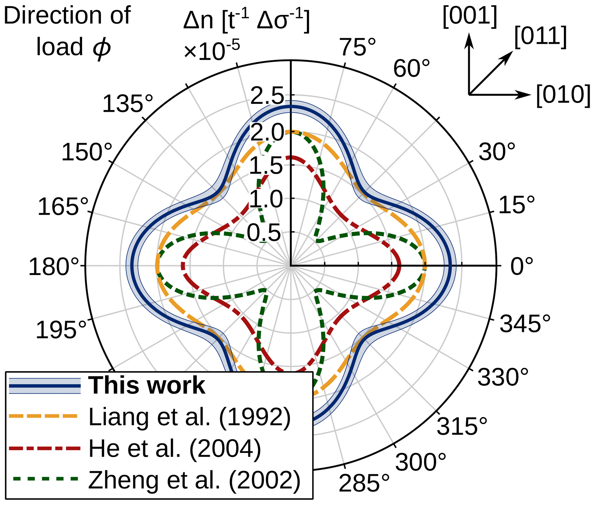
Figure 9Comparison of the model derived using parameters determined in this study to works from the literature. Shear stresses are neglected (σ12=0).
The sign of the stress-optical parameters depends on the definition of the sign of tensile and compressive stresses. Tensile stresses are considered positive stresses in this work. However, due to the measurement principal, the sign of the measured retardation value can not be determined. Therefore, the stress-optical parameters are assumed to be positive. The signs of the stress-optical parameters from the literature in Table 1 are as reported in the studies listed.
Although the model has a similar shape to those in the studies by He et al. (2004) and Liang et al. (1992), the mathematical expressions differ between the models. This is despite the fact that all models stem from the same general approach for photoelasticity given by Neumann (1841) and Pockels (1889, 1906). Only for the isotropic case with parameters () are all models except for the model from Zheng and Danyluk (2002) identical. For this case, the models show the expected direction-independent stress-optical constant, as is shown in Fig. 10. The model from Zheng and Danyluk (2002) only becomes isotropic for a parameter combination of .
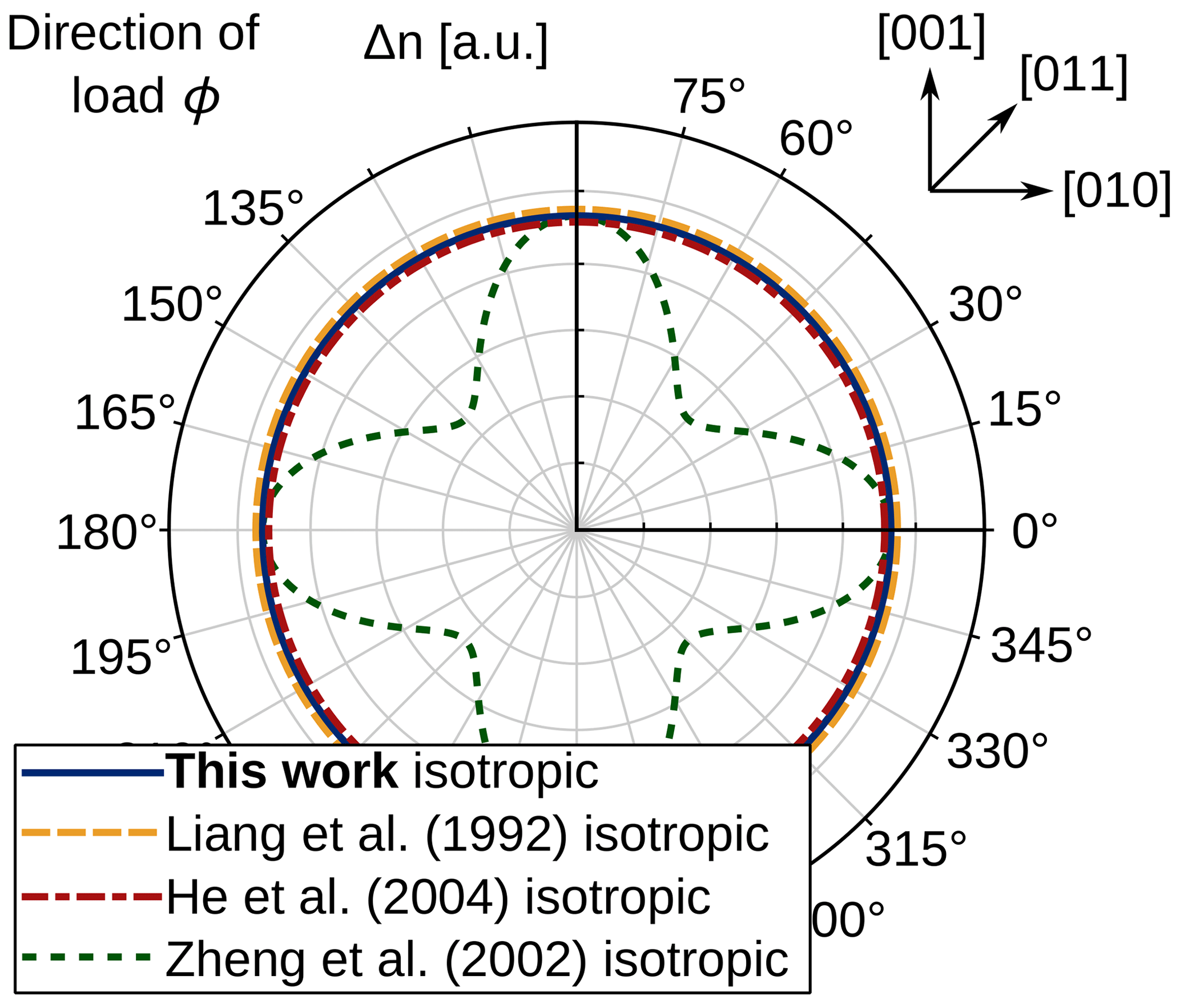
Figure 10Comparison of the model derived in this study to models from the literature for the isotropic case of .
For more detailed comparison, the rotated stress-optical tensors and derived in this work and in He et al. (2004), respectively, are identical, considering that the definition of the angle ϕ in He et al. (2004) is the angle between the [010] direction of the crystal lattice and the principal axis of the stress tensor. For Liang et al. (1992) and Zheng and Danyluk (2002), this correspondence could not be established. Additionally, Liang et al. (1992) derived the stress-optical law assuming that the direction of incident light is lying in plane to the plane stress. In the work of He et al. (2004), a simplification is made by stating that the principal direction of the stress tensor σij coincides with the principal direction of the impermeability tensor ΔBij. This allows for an easier theoretical determination of ΔBI and ΔBII. In practice, this means that at the principal direction of the impermeability tensor must first be measured (e.g. by measuring the isoclinic angle), and the stress-optical tensor πijkl must then be rotated accordingly. However, this assumption leads to a deviation of up to 4 % (8 % using the parameters determined by He et al., 2004) by ignoring off-diagonal terms of ΔBij. This deviation does not occur upon determination of ΔBI and ΔBII in an eigenvalue analysis in this work. The model from He et al. (2004) for Δn can be reduced to an expression where only the difference in principal stresses σI−σII occurs. The model derived in this work cannot be reduced to that. For this model, Δn is always dependent on the stresses σ11, σ22 and σ12.
Figure 7 shows a measured retardation for a loading direction of ϕ=45∘. Measurements with slight asymmetric retardation maps were also found. This can be caused by misalignment of the clamping jaws, i.e. the two opposite forces compressing the silicon wafer do not lay on the same axis. This can lead to a deviation in the stress field. However, the comparison of the different experimental set-up results showed no strong influence on the experimental results here. In general, numerical analyses indicated that even a small misalignment influences the values of π44 more strongly than (π11−π12).
Using the approach from Neumann (1841) and Pockels (1889, 1906) for describing stress-induced birefringence, a model was derived for the stress-optical effect in silicon. This model contains two independent stress-optical parameters (π11−π12) and π44. The stress-optical parameters were determined to be MPa−1 and MPa−1. using a Brazilian disc test and a finite element simulation. In total, 46 measurements were used to determine the parameters by loading a (100)-silicon wafer under different angles.
In appearance, the model derived shows a similar shape to those from Liang et al. (1992) and He et al. (2004). However, they differ with respect to their mathematical expression. The derivation of the stress-optical law from He et al. (2004) could be reproduced in part, while a simplification made by He et al. (2004) that introduces a certain error was not necessary in the model in this work. It determines the stress-optical law for a (100)-silicon wafer and, hence, allows for a more precise characterization of the mechanical stresses.
The determined parameter values are fairly large compared with those from the literature. However, considering the different sources of error in the experiment and simulation, the values here tend to increase rather than decreasing toward a better quantitative match with literature parameters. To get a closer match, either the measured retardation values need to be higher or the simulated stresses need to be lower. Unfortunately, neither the experimental or numerical steps indicate an approach toward this behaviour. Hence, this mismatch and the application of the model derived are the focus of further research.
The underlying measurement data and code used in this work can be requested from the authors if required.
MS derived the analytical models, devised the experiments, performed the experiments and wrote the article. GG, TH and SS offered advice on the article as well as reviewing it and recommending corrections.
The authors declare that they have no conflict of interest.
This article is part of the special issue “Sensors and Measurement Systems 2019”. It is a result of the “Sensoren und Messsysteme 2019, 20. ITG-/GMA-Fachtagung”, Nuremberg, Germany, 25–26 June 2019.
The authors are grateful to Christiane Schuster (Fraunhofer IKTS, Germany) and Ringo Köpge (Fraunhofer IMWS, Germany) for their support.
This research has been supported by the European Social Fund (grant no. K-7531.20/462-9).
This paper was edited by Thomas Fröhlich and reviewed by two anonymous referees.
Ajmera, P. K., Huner, B., Dutta, A. K., and Hartley, C. S.: Simulation and observation of infrared piezobirefringent images in diametrically compressed semiconductor disks, Appl. Opt., 27, 752–757, https://doi.org/10.1364/AO.27.000752, 1988. a
Brewster, D.: On the Effects of Simple Pressure in Producing That Species of Crystallization Which Forms Two Oppositely Polarised Images, and Exhibits the Complementary Colours by Polarised Light, Philos. T. Roy. Soc. Lond., 105, 60–64, 1815. a
Brewster, D.: On the Communication of the Structure of Doubly Refracting Crystals to Glass, Muriate of Soda, Fluor Spar, and Other Substances, by Mechanical Compression and Dilatation, Philos. T. Roy. Soc. Lond., 106, 156–178, 1816. a
Brito, M. C., Alves, J. M., Serra, J. M., Gamboa, R. M., Pinto, C., and Vallera, A. M.: Measurement of residual stress in EFG ribbons using a phase-shifting IR photoelastic method, Sol. Energ. Mater. Sol. Cell., 87, 311–316, https://doi.org/10.1016/j.solmat.2004.07.028, 2005. a
Ganapati, V., Schoenfelder, S., Castellanos, S., Oener, S., Koepge, R., Sampson, A., Marcus, M. A., Lai, B., Morhenn, H., Hahn, G., Bagdahn, J., and Buonassisi, T.: Infrared birefringence imaging of residual stress and bulk defects in multicrystalline silicon, J. Appl. Phys., 108, 063528, https://doi.org/10.1063/1.3468404, 2010. a
Giardini, A. A.: Piezobirefringence in Silicon, Am. Mineralog., 43, 249–262, 1958. a, b
He, S., Zheng, T., and Danyluk, S.: Analysis and determination of the stress-optic coefficients of thin single crystal silicon samples, J. Appl. Phys., 96, 3103–3109, https://doi.org/10.1063/1.1774259, 2004. a, b, c, d, e, f, g, h, i, j, k, l, m
Hecht, E.: Optik, 7th Edn., De Gruyter, Berlin, Boston, https://doi.org/10.1515/9783110526653, 2018. a
Herms, M., Irmer, G., Kupka, G., and Wagner, M.: The Photo‐Elastic Constant of Silicon Reviewed in Experiment and Simulation, Physica Status Solidi (a), 216, 1900254, https://doi.org/10.1002/pssa.201900254, 2019. a
Horn, G., Lesniak, J., Mackin, T., and Boyce, B.: Infrared grey-field polariscope: A tool for rapid stress analysis in microelectronic materials and devices, Rev. Scient. Instrum., 76, 045108, https://doi.org/10.1063/1.1884189, 2005. a, b
Jagailloux, F., Valle, V., Dupré, J.-C., Penot, J.-D., and Chabli, A.: Applied Photoelasticity for Residual Stress Measurement inside Crystal Silicon Wafers for Solar Applications, Strain, 52, 355–368, https://doi.org/10.1111/str.12185, 2016. a
Krüger, C., Heinert, D., Khalaidovski, A., Steinlechner, J., Nawrodt, R., Schnabel, R., and Lück, H.: Birefringence measurements on crystalline silicon, Class. Quant. Grav., 33, 015012, https://doi.org/10.1088/0264-9381/33/1/015012, 2016. a, b
Lederhandler, S. R.: Infrared Studies of Birefringence in Silicon, J. Appl. Phys., 30, 1631–1638, https://doi.org/10.1063/1.1735026, 1959. a
Liang, H., Pan, Y., Zhao, S., Qin, G., and Chin, K. K.: Two‐dimensional state of stress in a silicon wafer, J. Appl. Phys., 71, 2863–2870, https://doi.org/10.1063/1.351017, 1992. a, b, c, d, e, f, g, h
Narasimhamurty, T. S.: Photoelastic and Electro-Optic Properties of Crystals, 1st Edn., Springer US, Boston, MA, https://doi.org/10.1007/978-1-4757-0025-1, 1981. a, b, c, d, e
Neumann, K. E.: Die Gesetze der Doppelbrechung des Lichts in comprimirten oder ungleichförmig erwärmten unkrystallinischen Körpern, Ann. Phys. Chem., 130, 449–476, https://doi.org/10.1002/andp.18411301203, 1841. a, b, c, d, e
Pockels, F.: Ueber den Einfluss elastischer Deformationen, speciell einseitigen Druckes, auf das optische Verhalten krystallinischer Körper, Ann. Phys., 273, 269–305, https://doi.org/10.1002/andp.18892730604, 1889. a, b, c, d, e
Pockels, F.: Lehrbuch der Kristalloptik, 1st Edn., B. G. Teubner, Leipzig, available at: https://books.google.de/books?id=AkcNAAAAYAAJ (last access: 5 March 2018), 1906. a, b, c, d, e
Ramesh, K.: Digital Photoelasticity, 1st Edn., Springer, Berlin, Heidelberg, https://doi.org/10.1007/978-3-642-59723-7, 2000. a, b, c
Vivek, R. and Ramesh, K.: Residual Stress Analysis of Commercial Float Glass Using Digital Photoelasticity, Int. J. Appl. Glass Sci., 6, 419–427, https://doi.org/10.1111/ijag.12106, 2015. a
Wolf, H.: Spannungsoptik: Ein Lehr- und Nachschlagebuch für Forschung, Technik und Unterricht, 1st Edn., Springer, Berling, Heidelberg, available at: https://books.google.de/books?id=1z6nBgAAQBAJ (14 September 2019), 1961. a, b, c
Zheng, T. and Danyluk, S.: Study of Stresses in Thin Silicon Wafers with Near-infraredphase Stepping Photoelasticity, J. Mater. Res., 17, 36–42, https://doi.org/10.1557/JMR.2002.0008, 2002. a, b, c, d, e, f, g
Zinth, W. and Zinth, U.: Optik, 2nd Edn., Oldenbourg Verlag, München, 2009. a, b
- Abstract
- Introduction
- Theoretical analysis: photoelasticity in {100} silicon
- Measurement of stress-optical coefficients
- Discussion
- Summary and conclusion
- Code and data availability
- Author contributions
- Competing interests
- Special issue statement
- Acknowledgements
- Financial support
- Review statement
- References