the Creative Commons Attribution 4.0 License.
the Creative Commons Attribution 4.0 License.
 | 10 Aug 2022
Design of a CMOS memristor emulator-based, self-adaptive spiking analog-to-digital data conversion as the lowest level of a self-x hierarchy
Hamam Abd
Andreas König
The number of sensors used in modern devices is rapidly increasing, and the interaction with sensors demands analog-to-digital data conversion (ADC). A conventional ADC in leading-edge technologies faces many issues due to signal swings, manufacturing deviations, noise, etc. Designers of ADCs are moving to the time domain and digital designs techniques to deal with these issues. This work pursues a novel self-adaptive spiking neural ADC (SN-ADC) design with promising features, e.g., technology scaling issues, low-voltage operation, low power, and noise-robust conditioning. The SN-ADC uses spike time to carry the information. Therefore, it can be effectively translated to aggressive new technologies to implement reliable advanced sensory electronic systems. The SN-ADC supports self-x (self-calibration, self-optimization, and self-healing) and machine learning required for the internet of things (IoT) and Industry 4.0. We have designed the main part of SN-ADC, which is an adaptive spike-to-digital converter (ASDC). The ASDC is based on a self-adaptive complementary metal–oxide–semiconductor (CMOS) memristor. It mimics the functionality of biological synapses, long-term plasticity, and short-term plasticity. The key advantage of our design is the entirely local unsupervised adaptation scheme. The adaptation scheme consists of two hierarchical layers; the first layer is self-adapted, and the second layer is manually treated in this work. In our previous work, the adaptation process is based on 96 variables. Therefore, it requires considerable adaptation time to correct the synapses' weight. This paper proposes a novel self-adaptive scheme to reduce the number of variables to only four and has better adaptation capability with less delay time than our previous implementation. The maximum adaptation times of our previous work and this work are 15 h and 27 min vs. 1 min and 47.3 s. The current winner-take-all (WTA) circuits have issues, a high-cost design, and no identifying the close spikes. Therefore, a novel WTA circuit with memory is proposed. It used 352 transistors for 16 inputs and can process spikes with a minimum time difference of 3 ns. The ASDC has been tested under static and dynamic variations. The nominal values of the SN-ADC parameters' number of missing codes (NOMCs), integral non-linearity (INL), and differential non-linearity (DNL) are no missing code, 0.4 and 0.22 LSB, respectively, where LSB stands for the least significant bit. However, these values are degraded due to the dynamic and static deviation with maximum simulated change equal to 0.88 and 4 LSB and 6 codes for DNL, INL, and NOMC, respectively. The adaptation resets the SN-ADC parameters to the nominal values. The proposed ASDC is designed using X-FAB 0.35 µm CMOS technology and Cadence tools.
- Article
(20699 KB) - Full-text XML
- BibTeX
- EndNote


In the last few years, both diversity and the number of deployed sensors have significantly increased due to the rapid advancement of artificial intelligence and machine learning in the internet of things (IoT) and Industry 4.0 (Werthschützky, 2018; Meijer, 2008). The performance of the intelligent sensor faces a lot of issues due to static and dynamic variations. These issues are effectively addressed by using reconfigurable structures with the self-X (self-calibration, self-optimization, and self-healing) properties (Alraho et al., 2020; Zaman et al., 2021; Aamir et al., 2018; Jo et al., 2019; Lee et al., 2018b; Lu et al., 2013; Koenig, 2018). However, reconfigurable structures are still utilizing amplitude-coded signals that face issues with downscaling technologies. These advocate the design of an electronic sensor system robust to technology scaling and self-x properties to compensate for the static and dynamic variations implemented by a time-coded signals system with self-x properties. This motivated a spiking neural network (SNN) concept inspired by the biological neural network, where the information is encoded by spike timing and will not be vulnerable to the issues concerning technology scaling (Guo et al., 2021; Henzler, 2010a; Staszewski et al., 2005). A key mandatory element of the SNN is the synapse which can be emulated by the memristor, and the memristor can considerably improve SNN (Lv et al., 2018; Zhang et al., 2020). The memristor can thrust new computing systems beyond Moore's law (Mehonic et al., 2020; Zidan et al., 2018). The memristor enhances the capability of the self-adaptive analog frontend sensory electronics, especially for the application design with advanced-node complementary metal–oxide–semiconductor (CMOS) technology (Zidan et al., 2018). The memristor architectures supply a small on-chip footprint (Graves et al., 2020), low power profile (Graves et al., 2020; Shchanikov et al., 2021), machine learning, and artificial intelligence (Kim et al., 2021; Krestinskaya et al., 2019; Li et al., 2020; Midya et al., 2019; Manouras et al., 2021; Shchanikov et al., 2021). Machine learning supports the configurable electronic circuits to have self-x properties and a flexible platform for IoT and Industry 4.0 (Koenig, 2018).
Numerous researchers have concentrated on implemented emulating biological synapses to implement a neuromorphic system that performs closer to biological neural network sensors (Berdan et al., 2016; Burr et al., 2017; Covi et al., 2019; Kim and Lee, 2018a; Ohno et al., 2011; Yang et al., 2017). Recently, some researchers concentrated on achieving the synapse function by memristor (Kim et al., 2018; Park et al., 2020). In biological synapses, two types of synaptic plasticity, namely long-term plasticity (LTP) and short-term plasticity (STP; Kandel, 2000; Martin et al., 2000), are observed. Kim et al. (2015), Li et al. (2013), Mannan et al. (2021), Wang et al. (2017), Wu et al. (2021), Zhang et al. (2017), Yang et al. (2018), and Ren et al. (2018) constructed memristors to emulate both long-term plasticity (LTP) and short-term plasticity (STP) adaptation functions of the synapses.
There are several challenges to implementing the SNN inspired by biological neural sensors systems based on memristor as a synapse, such as reliability, compatibility with CMOS technology, the fabrication complexity of memristor systems, the lifetime of memristor devices, the finite number of resistance levels, and resistance level stability (Krestinskaya et al., 2019; Zhang et al., 2020). Therefore, one more class of researchers have focused on memristor emulators to implement memristor SNN architectures on contemporary chips (Babacan et al., 2017; Cao and Wang, 2021; Kanyal et al., 2018; Prasad et al., 2021; Sánchez-López et al., 2014; Yadav et al., 2021; Abd and König, 2020, 2021b). Compared to the CMOS-based memristor, the material-based type offers more advantages beyond Moore technology to support a much more compact design and less power consumption.
State-of-the-art designs have complex circuits, utilize a large number of active and passive components, and demand an external device. Babacan et al. (2017) proposed a memristor with a multi-output operational transconductance amplifier (MO-OTA), multiplier, capacitor, and resistor. Also, in Cao and Wang (2021), they proposed a memristor circuit using an operational amplifier, multiplier, sine converter, resistor, and capacitor. Additionally, Kanyal et al. (2018) proposed a memristor circuit utilizing two operational transconductance amplifiers (OTA) and one capacitor. Similarly, in Prasad et al. (2021), they proposed a memristor circuit built with a Z-copy current follower transconductance amplifier (ZC-CFTA) and capacitor. Likewise, Sánchez-López et al. (2014) proposed a memristor emulator with a single multiplier and four second generation current conveyors (CCII). Yadav et al. (2021) also proposed a memristor circuit utilizing a fully balanced voltage differencing buffered amplifier (FB-VDBA) and capacitor. They emulated the LTP function by utilizing external memory, digital-to-analog converter (DAC), and a big external capacitor. Yadav et al. (2021) detached the information processing and memory that sent back the design to the restriction of the Von Neumann (1945) computing architecture. It needs a shuttling of information between two units, consuming more power, and is a slow process. Shuttling becomes a severe problem when an extensive system is implemented. In contrast, the biological nervous system combines memory and information processing, and consequently, it can process complex information and have ultralow power consumption (Berdan et al., 2016). Artificial synapses that mimic STP and LTP of the biological synapses are required to implement neuromorphic systems, mimicking the biological nervous system (Kim and Lee, 2018b).
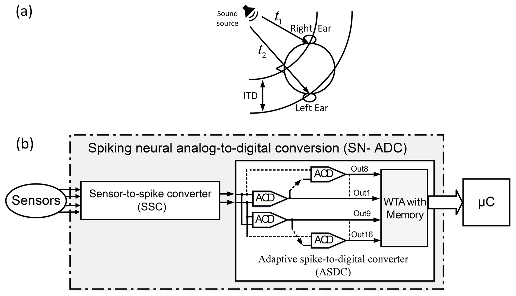
Figure 1(a) Acoustic localization model. The brain uses the interaural time differences (ITDs) between the two signals arriving at the ears, t1−t2, to locate the voice's position, where t2 and t1 are the times of the voice arriving at the left and right, respectively. (b) Neuromorphic signal conditioning architecture. Sensor-to-spike conversion (SSC) transfers the sensor signal into two spikes at different times, depending on the sensor signal. The adaptive spike-to-digital converter (ASDC) block generates digital code based on this time difference between the spikes. The ASDC has two main blocks, namely adaptive coincidence detection (ACD) and winner-take-all (WTA), with memory.
This work represents one building block of our concept on robust adaptive spiking sensor systems, focusing in this paper on the adaptive spike-to-digital conversion. This concept, as already indicated in our previous work, needs a prior stage denoted as sensor-to-spike conversion (SSC; Kammara and König, 2016, 2014b; Kammara and Koenig, 2014a; König and Kammara, 2017; Subramanyam and Chandra, 2017). Early work done by the second author is on a light-to-frequency or light-to-spike-code converter in the CMOS image sensor (Doge et al., 2002). In the latter case, and in similar work following up on ours in the literature, the incident light information was transduced to rate code representation. In more recent work by Kammara and König (2016), Kammara and König (2014b), Kammara and Koenig (2014a), König and Kammara (2017), and Subramanyam and Chandra (2017), this was extended to further sensor modalities and the time to the first spike coding and its extension to differential representation.
Living beings own a remarkable sensing capability for physical and chemical quantities (Leitch et al., 2013; Stieve, 1983). They also possess an adaptability according to environmental conditions and occurring faults or lesions. The neural network creates the key to this regulation. The sensory systems in living beings concentrate on possessing thousands of sensors linked to peripheral neural ensembles.
The acoustic localization is an exception to that. It localizes the objects, predator, prey, water, or food by spatially detached paired sensors (Ashida and Carr, 2011; Carr and Konishi, 1988, 1990; Grothe et al., 2010; Seidl et al., 2010; Carr and Christensen-Dalsgaard, 2015). Living beings use the time difference between signals arriving at the two ears, which we call interaural time differences (ITDs) to locate the sound source, and it can be represented in an array of nerve cells as a place. The place theory was presented by Jeffress (1948). Jeffress (1948)'s theory builds on the following three essential assumptions (Ashida and Carr, 2011): (1) an orderly arrangement of ascending nerve fibers in the conduction times which act as delay lines, (2) then an array of coincidence detectors convert input synchronization to output spike rates, and, finally (3), form a neuronal place map within the cell array by using systematic variation in spiking rates. The architecture and design of neuromorphic systems try to emulate the biological nervous system structures. Delay lines in acoustic localization are an explicit model of adaptive SNN architecture, as shown in Fig. 1a. It can be utilized for spiking neural analog-to-digital conversion (SN-ADC). The implementation of an SN-ADC inspired by human hearing acoustic localization demands two segments, i.e., the sensor-to-spike converter (SSC) and spike-to-digital converter (SDC) (Kammara and König, 2016). The SSC transforms the sensor signal into two spikes with the time difference. Based on this time difference between the spikes, the SDC block generates digital code. The prior implementation of the ADC did not make use of adaptivity as desired, e.g., to transact with static and dynamic variations and technology scaling issues (Kammara and König, 2016). Dynamic and static variations forcefully challenge the performance of the sensor (Lee et al., 2018a; Lin et al., 2019). Static variations are due to processed parameter deviations, mechanical stress due to packaging, and lithographic uncertainties, while the dynamic variations are due to the dynamic operating condition of the circuit with the supply voltage variation and the ambient temperature. On the other hand, the long-term aging effect on the circuit elements adds a shift to the circuit performance with the passage of time (Alraho et al., 2020).
We proposed a system in Fig. 1b to mimic the model of sound localization proposed by Jeffress (1948). The first block in Fig. 1b, SSC, transfers the sensor signal into two spikes with ITDs, where the value of the ITDs will depend on the sensor signal. The second block in Fig. 1b, the adaptive spike-to-digital converter (ASDC), has the three essential assumptions of Jeffress (1948)'s theory. Where the weights of the synapses implement the first one, the second is implemented by an array of the adaptive coincidence detection (ACD), which converts the ITDs of the two input pulses to the rank spike code, and the third is implemented by winner-take-all (WTA) with memory, which converts the rank spike code to the digital code. The primary goal of this work is to implement the ASDC, which is the fundamental building block of SN-ADC, to demonstrate that the conceived structure and adaptation algorithm can cope with the worst-case deviations of the regarded implementation technology. In this design, we used the MOSFET 3.3 V main model of the 0.35 µm CMOS technology by X-FAB. The novel contributions of our work are the (1) implementation of an adaptive spike-to-digital converter (ASDC) inspired by acoustic localization, (2) design of an adaptive spike-to-rank coding (ASRC) encoded by time to the first spike, (3) design of an adaptive coincidence detection (ACD) with self-adaptive properties, (4) realization of an adaptation method to adapt all ACDs at the same time, (5) implementation of CMOS memristors emulating the short- and long-term plasticity of biological synapses, (6) realization of the leaky integrate-and-fire (LIF) neuron with more cost-effective design and producing the ACD properties, (7) implementation of the winner-take-all (WTA) circuit and memory with a more efficient design, and (8) proposition of an algorithm to convert the rank code to binary code.
Recently there has been a high demand for ADC in Industry 4.0 and IoT to perform under a dynamic environment and overcome the issues of the conventional ADC in the amplitude domain. The implementation of ADC in the time domain can overcome these issues (Henzler, 2010a; Staszewski et al., 2005). The implementation of ADC in the spike representation (time domain) has a high variance in its parameter due to static and dynamic variations. Therefore, it is essential to implement the ADC with adaptation to compensate for the deviation. Therefore, we propose the design of SN-ADC based on time coding with self-adaptation.
The proposed SN-ADC has two parts, SSC and ASDC, as shown in Fig. 7. The ASDC is based on the ACD, which has two parts adaptive synapse (AS) and neuron. In total, our designed SN-ADC has 32 synapses and 16 neurons. Every synapse has an 8 bit binary digitized transistor and vg variable to control its weight, as shown in Fig. 2. Also, every neuron has two adaptation variables. In total, the current work has 96 variables. We have built the SN-ADC with two layers of the adaptation hierarchy, as shown in Fig. 7. The first layer is at the level of ACD, and the second layer is at the level of ASDC.
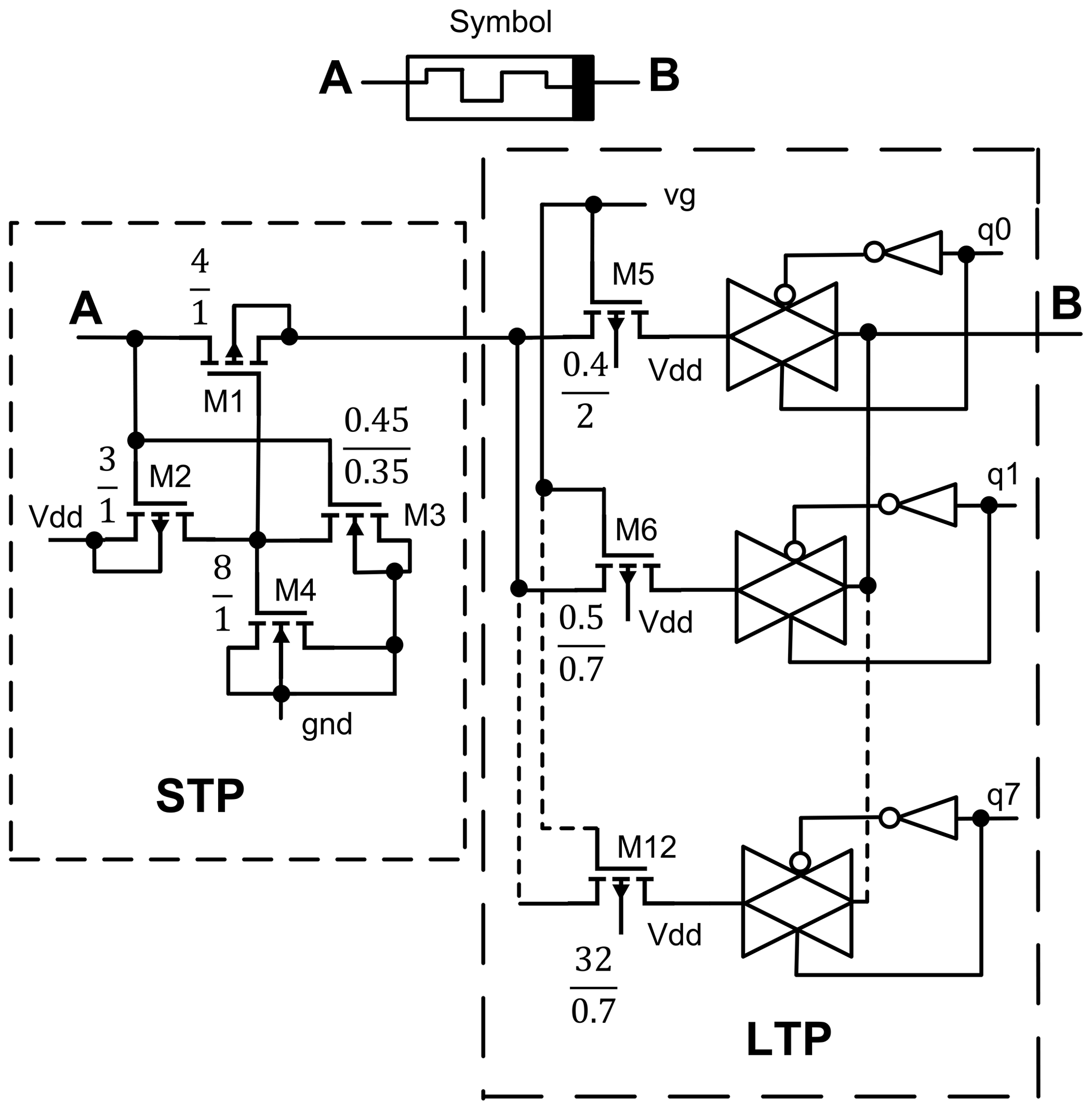
Figure 2CMOS memristor mimics the synaptic plasticity, long-term plasticity (LTP), and short-term plasticity (STP) of biological synapses. This circuit represents the adaptive synapse (AS) of our proposed structure (sizes of the transistors are in µm).
The first layer of the adaptation hierarchy is designed and presented in this work. In this layer, the adaptation circuit automatically adapts the synapses' weight and reduces it from 96 variables to only four variables, i.e., VLEAK, VRFR, vg1, and vg2. In the first layer, the adaption runs simultaneously for all ACD in parallel; hence, the number of exposed variables for each individual synapse and neuron is equivalent to one ACD, where the ACD has four variables, i.e., VLEAK, VRFR, vg1, and vg2. Those four variables in the current stage of development of our design have been adapted manually. In the future, machine learning can automatically help us to control the four voltage variables. Alternative to software implementation, the design of a circuit to control these variables could be considered a second layer of the adaptation hierarchy. Hence, the whole circuit can be automatically adapted by using only those four variables instead of 96 variables. This would help to reduce the complexity of the adaption circuit and require less adaptation time. The second top adaptation layer runs over the first layer, and it is responsible for changing only the variables of VLEAK, VRFR, vg1, and vg2. For every change in those variables, the first layer took part in the adaptation process, and the second layer waited until the first layer finished with the solution. If the solution succeeds in correcting the synapse weight, then the adaptation process ends; otherwise, the second layer updates the variables (VLEAK, VRFR, vg1, and vg2) and runs the adaptation for the next round and so on.
3.1 Adaptive synapse (AS)
This work presents an adaptive synapse that mimics the LTP and STP of biological synapses. These are established on the CMOS memristor presented in Fig. 2. Transistors from M5 to M12 perform the LTP, and the transistors from M1 to M4 perform the STP. M2 and M3 transistors work as feedback circuits and control the voltage across M4. The M4 transistor operates as a capacitor by tying together the source, drain, and bulk. The voltage current characteristic of the proposed memristor in shown Fig. 35 for 4 MHz frequency.
3.2 Neuron
There are various biological neuron models with numerous properties. We look at the features required for our proposed coincidence detection to work as a neural network time delay with an inverse relationship between the magnitude of incoming charge and the time to the first spike. These are essential features provided with any spiking neuron model.
To meet the requirements of this work with a lower number of adaptation variables and transistors, we modified and removed the unnecessary components of the LIF neuron (Indiveri, 2003) for this work. Indiveri's LIF analog neuron model has elements for setting an arbitrary refractory period, spike frequency adaptation, modulating the neuron's threshold voltage, positive feedback, membrane capacitor, a transistor for a current leak, and a digital inverter for generating a pulse. This neuron circuit appears to be very flexible; the focus of this design was to mimic biological neurons. It results in many adaptation variables and a high number of transistors.
The element for modulating the neuron's threshold voltage in the Indiveri model is used to control the threshold voltage of the neuron. On the other hand, the threshold provided by CMOS transistors (M3 and M4) obtains the desired results for this work. Therefore, this element is removed to minimize the number of adaptation variables and transistors. The element for spike frequency adaptation is used to control the frequency of the spikes for continuous inputs (or for the same signal). However, this work does not require a spike frequency adaptation property. This work looks at the features required for our proposed coincidence detection to function as a neural network time delay with an inverse relationship between the magnitude of the incoming charge and the time to the first spike. Therefore, this element is removed to minimize the number of adaptation variables and transistors.
The element of positive feedback increases the potential membrane speed, leading to reaching the neuron threshold in a shorter time. Therefore, it makes the inverter (M3 and M4) switch rapidly and reduces the power dissipation. However, this affects the features of this work, which is an inverse relationship between the magnitude of the incoming charge and the time to first spike. Therefore, this element is also removed.
Our proposed neuron circuit has 16 transistors and two variables compared to the Indiveri model, which has 20 transistors and four variables. Therefore, this simplifies our proposed neuron's adaptation process compared to the adaptation with four variables for the Indiveri model. This results in a speed gain of eight, a power consumption decrease by 20 %, an area decrease by 30 %, and a spike rate increase by 8 times, compared to the Indiveri model.
The modified model circuit shown in Fig. 3. The membrane capacitor C is charged by the current from the synapses. When the voltage of the capacitor is higher than the crossing point voltage of the inverter (M3 and M4) transistors, it triggers the second inverter (M6 and M7). The VRFR controls the pulse width of the neuron output and the inverter (M6 and M7), which is used to produce the output and discharge the capacitor, respectively.

Figure 3Proposed circuit of analog leaky integrate-and-fire (LIF) neuron (sizes of the transistors are in µm). It is simplified from Indiveri's neuron by removing the unnecessary components for the target of this work. It is used to implement adaptive coincidence detection (ACD) block.
Meanwhile, the M1 is leaking the capacitor based on the VLEAK value. The transistor sizes are tuned during the design process of ASRC to produce the spike order codes that still function correctly against the process, voltage, and temperature (PVT) corners listed in Table 3. The transistors sizes are shown in Fig. 3.
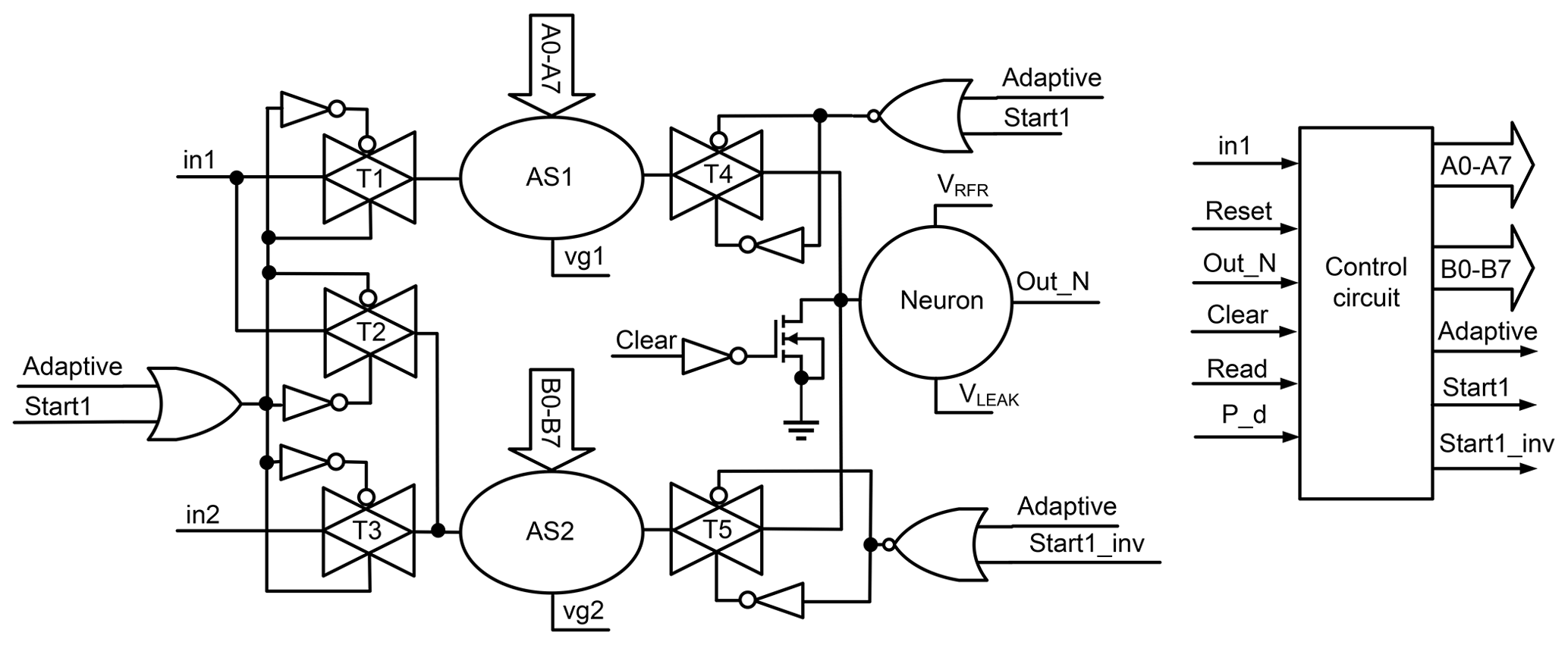
Figure 4The proposed adaptive coincidence detection (ACD) scheme is implemented with two adaptive synapses (ASs) and one neuron. The control circuit implements the self-adaptive method for the weights of the synapses. The transmission gates T1–T5 are used to connect and disconnect the ASs during the adaptation of their weights.
3.3 Adaptive coincidence detection (ACD)
The primary portion of the ASRC is the ACD implemented by one neuron and two adaptive synapses, as presented in Fig. 4. In the prior implementation of the ACD, the weight of the synapse was adaptive by an up–down counter (Abd and König, 2021a). The adaptation time increases exponentially with the increase in the synapses number. In this work, we have introduced a self-adaptive method for the synapses. It adapts the weights of the synapses of all ACDs at the same time. The adaptation time is exponentially decreased compared with the previous work.

Figure 5Proposed scheme of adaptive spike-to-rank coding (ASRC). Adaptive coincidence detection (ACD) is the essential block of the ASRC. The ASRC generates spikes that order codes according to the difference in time amount between the two spikes at its inputs.
The proposed ASRC is implemented by 16 ACDs, as shown in Fig. 5. The ASRC has two symmetrical parts, i.e., the upper and lower parts. The upper part ACDs produce the ASRC outputs from Out1 to Out8, while the lower part ACDs produce the ASRC outputs from Out9 to Out16. The ASRC has two inputs, namely in1 and in2. The in1 in the upper part is connected directly to the ACDs' first input, while the in2 is passed through the ACDs, one by one, representing the upper part's delay chains. The lower part, in2, is connected directly to the ACDs' first input, while the in1 passed the ACDs one by one, representing the lower part's delay chains.
The time of the delay chain unit is determined by the time of the neuron fire, which is controlled by the input current of the neuron. Nevertheless, the input current of the neuron is adapted by synapse weight. Consequently, the synapses' weights adapt to the unit delays throughout the delay chain despite deviations occurring.
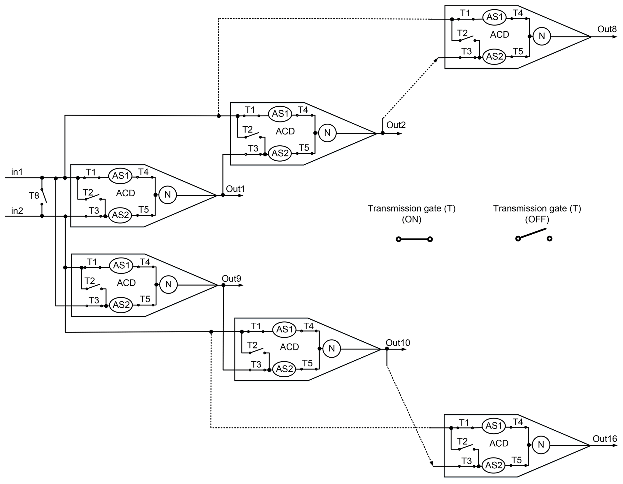
Figure 6This figure shows that the ASRC has a normal and adaptation mode. In the normal mode, both synapses of the ACD are connected to the neuron. The switching state of the transmission gates in the normal mode, T1, T3, T4, and T5, are on, and T2 and T8 are off. The adaptation mode has two states. Only the first synapse is connected to the neuron in the first state. The switching state of the transmission gates in the first state of the adaptation mode, T1, T4, and T8, are on, and T2, T3, and T5 are off. Only the second synapse is connected to the neuron in the second state. The switching state of the transmission gates in the second state of the adaptation mode, T2, T5, and T8, are on, and T1, T3, and T4 are off.
3.4 Operation modes of ASRC
The ASRC has two operation modes; the first is the normal mode, when both synapses of the ACD are connected to the neuron. The second mode is the adaptation mode and has two states. The first state is for adapting the first synapse's weight, where only the first synapse is connected to the neuron, as indicated in Fig. 6. The second state adapts the second synapse's weight, where only the second synapse is connected to the neuron, as indicated in Fig. 6. In the adaptation mode, the transmission gate (T8) connects in1 to in2, as displayed in Fig. 6. Therefore, in1 is used to adapt the weights of the synapses. In the first state of the adaptation mode, the first synapses of all ACDs are connected in parallel (one column) to the in1 and adapt their weight simultaneously. In the second state of the adaptation mode, the second synapses of all ACDs are connected in parallel to the in1 and adapt their weights simultaneously. After the adaptation process is finished, the T8 is turned off, as shown in Fig. 6.
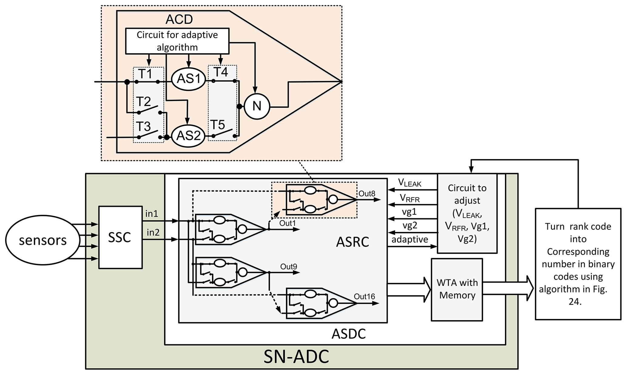
Figure 7Neuromorphic signal conditioning architecture. The spiking neural analog-to-digital data conversion (SN-ADC) has a two-part sensor-to-spike converter (SSC) and adaptive spike-to-digital converter (ASDC). The ASDC consists of adaptive spike-to-rank coding (ASRC), a winner-take-all (WTA) circuit with memory, and a circuit to control the variables VLEAK, VRFR, vg1, and vg2. The ASRC has 16 adaptive coincidence detections (ACDs), and every ACD has two adaptive synapses (ASs) and one neuron (N), as well as a circuit for the adaptive algorithm.
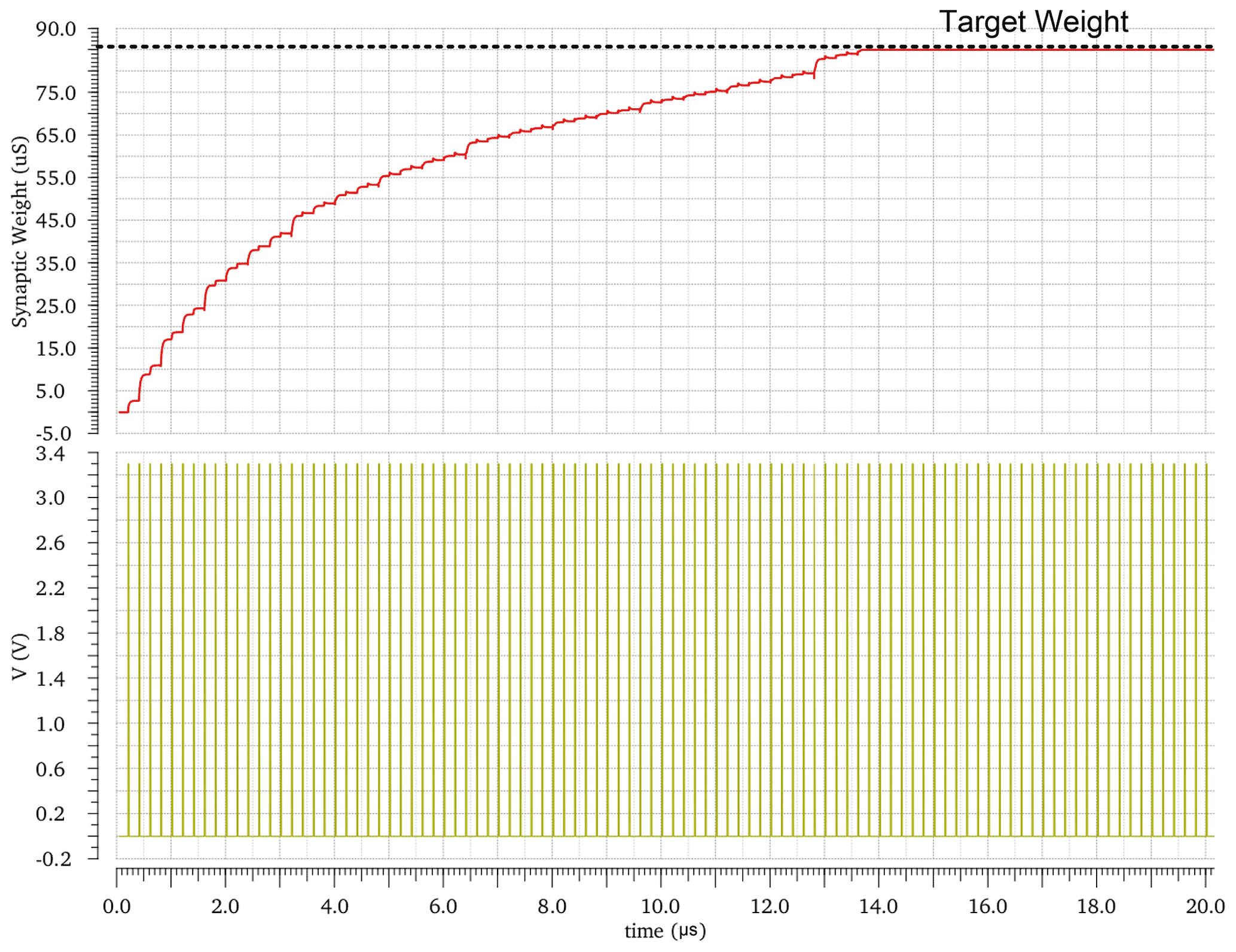
Figure 8This figure shows the adaptation work of the first layer. The weight of the first synapse of the first ACD is adapted until it reaches the target weight. The variables VLEAK, VRFR, vg1, and vg2 of the second layer are fixed to 700 mV, 800 mV, 1.8 V, and 220 mV, respectively. Circuit conditions are Vdd=3.3 V, and temperature is 27 ∘C and on the nominal process. The value can be different, depending on the present perturbation of the regarded corner.
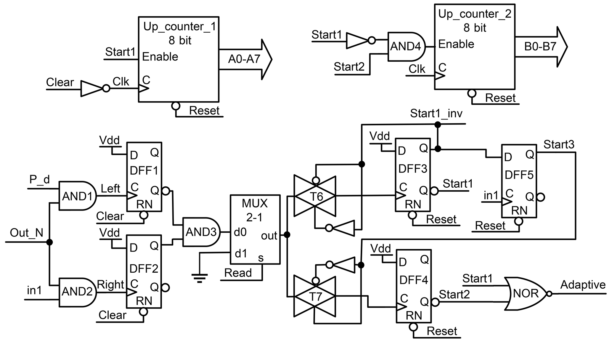
Figure 9The control circuit of adaptive coincidence detection (ACD). It implements the self-adaptive method for the synapses' weights and saves the synapses' weights on the up_counters.
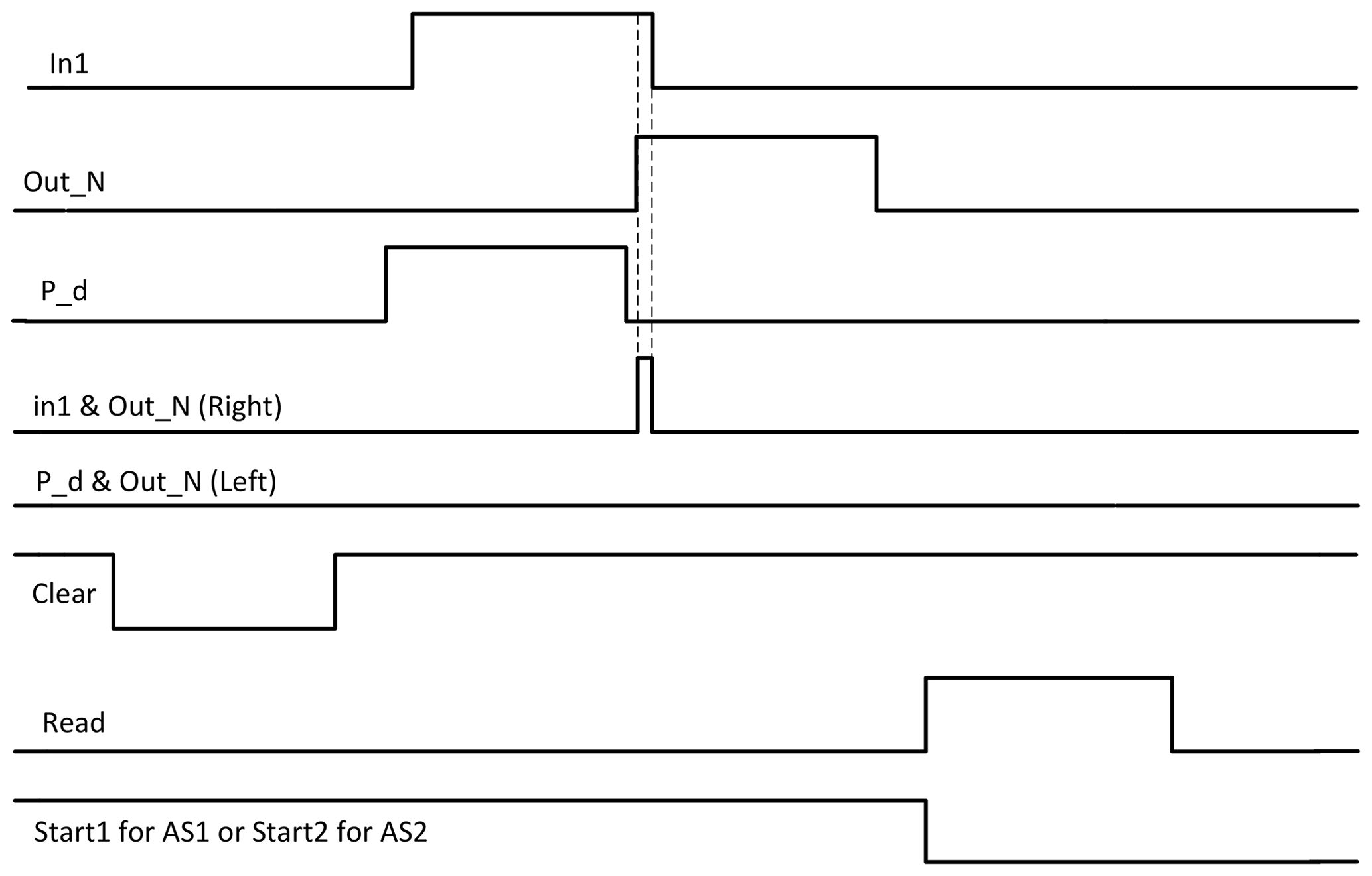
Figure 10The timing chart of adaptation synapse. There are two pulses that check the time of the neuron fire before and after the rising edge of the neuron pulse, i.e., P_d pulse and in1 pulse, respectively. If the neuron fires at a specific time, the right and left signals are 1 and 0. The Read signal is used to read after a specific time.
3.5 Adaptation process
The weight of the synapse determines the time of neuron fire. Therefore, the timing of the neuron's firing is proportional to the weight of the synapse. There are two pulses that check the time of neuron fire before and after the rising edge of the neuron pulse, P_d pulse, and in1 pulse, respectively. The output of the first AND gate (left) presented in Fig. 9 should be 0 if the neuron's output did not shift to the left, as shown in Fig. 10. The output of the second AND gate (right), shown in Fig. 9, should be 1 if the neuron's output did not shift to the right, as shown in Fig. 10. The D flip-flop 1 (DFF1) and DFF2 save the first and second AND gates' outputs (left and right shift). The first and second counters adapt and save the weights of the first and second synapses, respectively. The Clear input is used for several tasks. First, it is used to clear the DFF1 and DFF2 outputs and prepare them for the next weight check. Second, it is used to discharge the neuron capacitor. Third, it is used as a clock of the counter after inverting it. The multiplexer is used to pass the output of the AND3 gate at the specific time by setting the Read signal (selected from the multiplexer) to zero. The selection signal of the multiplexer becomes active after finishing the comparison of the signals (P_d, in1, and Out_N) and saving the results (left and right) on the DFF1 and DFF2.
The reset in the control circuit, indicated in Fig. 9, is used to reset the DFF3, DFF4, and DFF5. The Reset signal activates the adaptation mode. The DFF3 and DFF4 are used to save the adaptation weights of the first and second synapses. The output Adaptive signal of the first NOR gate is utilized to indicate the ACD is under self-adaptation when it is 0.
3.5.1 Adaptation mode: first state (adapting the weight of the first synapse)
The flow diagram of the ASRC models is displayed in Fig. 11. The adaptation starts by resetting the control circuit, and it starts adapting the weight of the first synapse. After the reset, counters are zero, and the Adaptive, Start3, and Start1_inv signals are 0, while the Start1 and Start2 signals are 1. These signals control the transmission gates (T1, T2, T3, T4, T5, T6, and T7), as illustrated in Figs. 4 and 9. Therefore, the T4 and T1 are on while T2, T3, and T5 are off. They connect the neuron to the first synapse and disconnect the second synapse. T1 passes the in1 to the first synapse. T2 disconnects in1 from the second synapse, and T3 disconnects in2 from the second synapse, as shown in Fig. 6. The Enable of the up_counter_1 and up_counter_2 are 1 and 0, respectively. T6 is on, and T7 is off. T6 connects the multiplexer output to the DFF3 clock, and T7 disconnects it from the DFF4 clock.
At the start of the adaptation process, a pulse signal is applied on the Clear input to clear the DFF1, DFF2, and discharge neurons capacitors and increase the counter_1 by one. Next, pulses are applied to the in1 and P_d inputs. Then, the neuron spike is checked by AND1 and AND2 gates to see if it has shifted to the left or right, and the result will be saved on DFF1 and DFF2, respectively. The negative output of the DFF1 and the Q output of DFF2 pass through the AND3 gate to the multiplexer.
After that, if the AND3 output gate is 0, the neuron's output shifts to the right or left, which means that the weight of the synapse did not reach the target weight. As a result, the adaptive weight of the first synapse continues, and the output of the AND3 gate passes through the multiplexer and transmission gate (T6) to the clock of the DFF3. In addition, Start1_inv and Start1 remain 0 and 1, respectively. Also, the transmission gate (T6) keeps connecting the output of the multiplexer to the DFF3. Moreover, the up_counter_1 Enable input remains 1, and the counter continues increasing with the next pulse on the Clear input. Furthermore, Start3 remains 0 with the next pulse on the in1, and the output of the multiplexer does not connect to the DFF4.
Figure 11Flow diagram of the adaptation layers' hierarchy. The first layer represents the adaptation work of adaptive ACD. The up_counter_1 and up_counter_2 save the 8 bit binary digitized transistor of the first and second synapses, respectively. Start1, Start1_inv, P_d, Start2, Start3, Adaptive, and Clear are signals used inside the control circuit of adaptive coincidence detection (ACD).
The ASRC remains in the first state of the adaptation mode, as shown in Fig. 6, until we reach the first synapse target weight. It makes the neuron fire between the P_d and in1 signals, and consequently, the AND3 gate becomes 1. After that, the outputs of DFF3 Start1_inv and Start1 become 1 and 0, respectively. As a result, they disconnect the multiplexer output from the DFF3 by turning T6 off. Also, they stop changing the synapse weight by disabling the up_counter_1, which means the adaptive weight of the first synapse is finished. In addition, they enable the up_counter_2. Moreover, they turn T1, T3, and T4 off and T2 and T5 on, as shown in Fig. 6, which leads to shifting the ASRC adaptation mode from the first state to the second state. Furthermore, Start3 becomes 1 with the next in1 pulse, connecting the multiplexer output to the DFF4 clock by turning T7 on.
3.5.2 Adaptation mode: second state (adapting the weight of the second synapse)
Similarly, the second synapse is adapted in the same way that the first synapse was adapted. Equally, the weight continues to change until the AND3 output becomes 1, which passes through multiplexer and T7 to the DFF4 clock. The negative output of DFF4 Start2 becomes 0. Then the output of the NOR gate, denoted Adaptive in Fig. 6, obtains the value 1. As a result, the Adaptive output shifts the ASRC from the adaptation mode second state to the normal mode by turning T1, T3, T4, and T5 on and T2 off, as shown in Fig. 6.
4.1 Adaptive coincidence detection (ACD)
The proposed ACD mimics three different states that generally occur in the biological neural systems, as displayed in Fig. 12. The first state produces an output spike if the input spikes occur at the same time. The second state produces an output spike if the input spikes occur slightly delayed. However, the output of the second state will produce a spike with a delay in contrast to the first state without a delay. The third state exhibits no spike when the two input spikes arrive with considerable delay. These states are the basis of acoustic localization in humans (Tavolga et al., 2012).
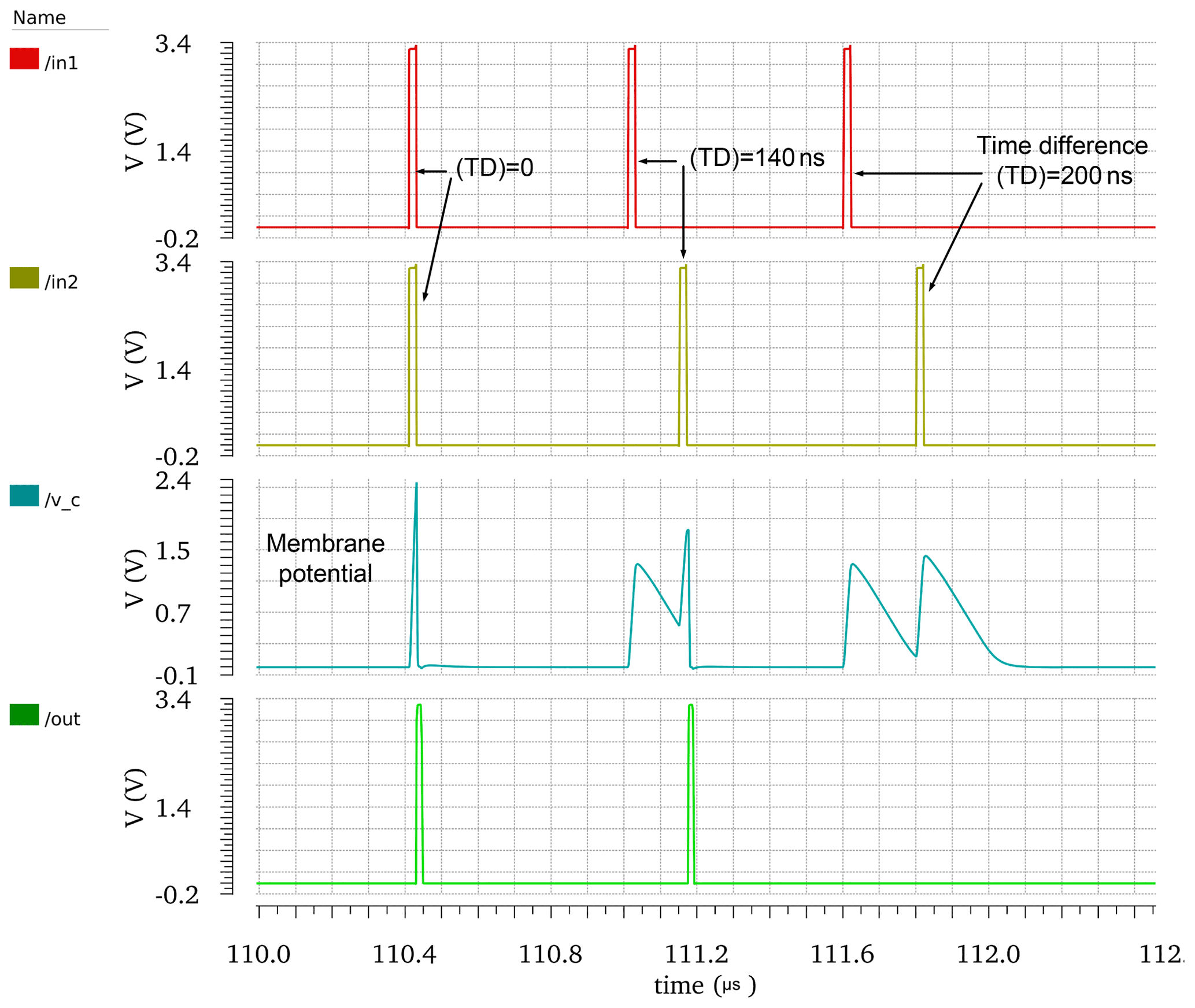
Figure 12Simulation of adaptive coincidence detection (ACD). It shows the concept of ACD. The timing of the generated output spike depends on the difference between the input pulses. When there is a considerable difference, then there will be no spike at the output.
4.2 First layer
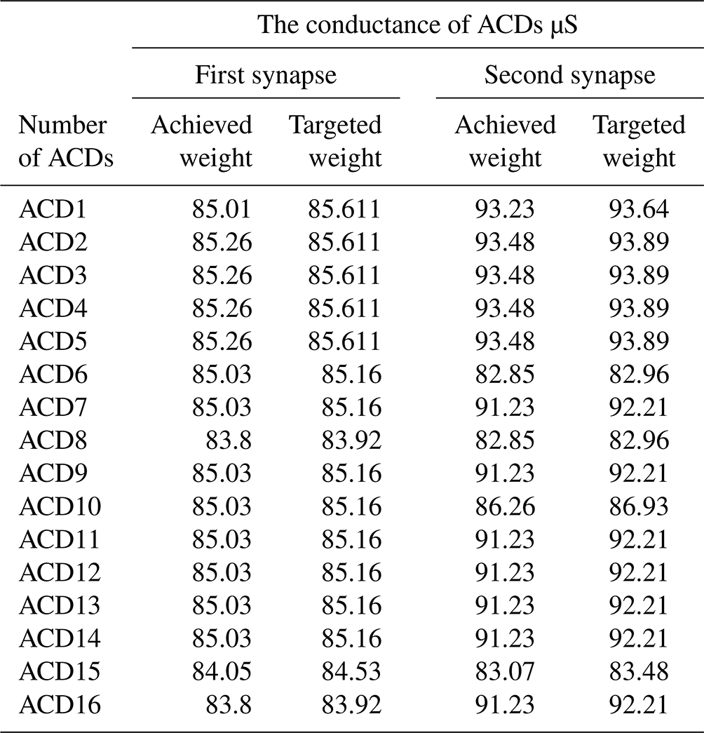
In this layer, the synapses' weights are automatically adapted. For the first layer, the up-counters start searching for the solution from zero until they find the solution. In order to show the adaptation of this layer, the variables VLEAK, VRFR, vg1, and vg2 of the second layer are fixed to 700 mV, 800 mV, 1.8 V, and 220 mV, respectively. Figure 8 shows how the first layer adapts the weight of the synapse until it reaches the desired weight. In Fig. 8, the y axis represents the conductance weight of the synapse, and the x axis shows the input pulse. It shows the adaptation of the first synapse of the first ACD. The results of the adaptation weights values of other synapses are shown in Table 5.
Figure 25 shows the difference between the desired and the actual value of the first synapse for the first ACD. The y axis represents an error. In the beginning, the error is 85.611 µS. It decreases with the passage of iterations until it reaches the desirable weight, with a residual error of 0.601 µS after 63 cycles. The number of cycles required by the adaptation process depends on the PVT conditions, while the upper limit of the number of cycles is 256.
4.3 Second layer
In the current work for the second layer, we do several manual iterations until we find the nominal solution, and this approach is working predictably. In the future, we will use machine learning or design a circuit to automate the second level of adaptation, so that the voltage values are no longer manually found and vulnerable in that sense. However, it will be instance specific and dynamically adapted in the wake of the automated correction procedure. Therefore, it will have invulnerability to process deviations and drift phenomena. The principle of the second adaptation layer is to fit the full-scale window of the 8 bit counter to the border of variation related to the PVT condition. In this way, the counter step sizes will be minimized, reducing the error representing the difference between the targeted value and the achieved level by the counter adaptation. It might be possible to think that one can fix the value of vg1 and vg2 to the maximum expected drift. However, this will increase the counter step size; hence, the error will be more significant for less PVT drift. In short, the purpose of the second adaptation layer is to smooth the counter step, where the latter one does the main optimization.
Figures 26–29 show the effect of vg1 and vg2 on the range of synapse weight, where vg1 influences the first synapse of all ACDs and vg2 has a same influence on the second synapse of all ACDs. However, those ranges will have the same number of steps in the first layer.
Synaptic LTP behaviors in Figs. 26–29 are achieved by 256 input pulses applied to the 8 bit counter, whose outputs control the 8 bit binary digitized transistor of the synapse. The LTP displays 256 states, and the LTP stays permanently, as long as the weight addressed by the counter does not change.
The variables VRFR and VLEAK affect the target weight of the synapse. In order to show their effect on the weight correction, we have fixed other variables and changed them, as shown in Figs. 30–34.

Figure 13The simulation of adaptive spike-to-digital converter (ASRC) rank coding, with in2 preceding in1. It represents the outputs of the ASDC at circuit conditions, where Vdd is 3.3 V, and temperature is 27 ∘C and on the nominal process. They are coded by spike order codes. Every column represents a different code and reflects the difference in time amount between the two spikes at inputs.

Figure 14The simulation of ASRC rank coding, with in1 preceding in2. It represents the outputs of the ASDC at circuit conditions, where Vdd is 3.3 V, and temperature is 27 ∘C and on the nominal process. They are coded by spike order codes. Every column represents a different code and reflects the difference in time amount between the two spikes at inputs.
Figures 30 and 31 show the effect of the VRFR on the target weight. The target weight changed from 54.5 to 64 µS by changing VRFR from 600 to 800 mV.
Figures 32, 33, and 34 show the effect of the VLEAK on the target weight. The target weight changed from 64 to 76.5 µS by changing VLEAK from 500 mV to 1.5 V.
4.4 Adaptive spike-to-rank coding (ASRC)
The ASRC will tend to generate spike orders that reflect the difference in time amount between the two spikes at its inputs. Spike order codes are coding schemes that use the pattern of spikes across a population of neurons. It depends on the order in which the neurons fire (Thorpe and Gautrais, 1998; Thorpe et al., 2001).
The proposed ASRC can achieve up to 16 different output spike orders. The time difference steps between in1 and in2 are from −120 to 120 ns in steps of 15 ns. Figure 13 displays the first eight time intervals where in2 precedes in1. Figure 14 displays the second eight time intervals where in1 precedes in2.
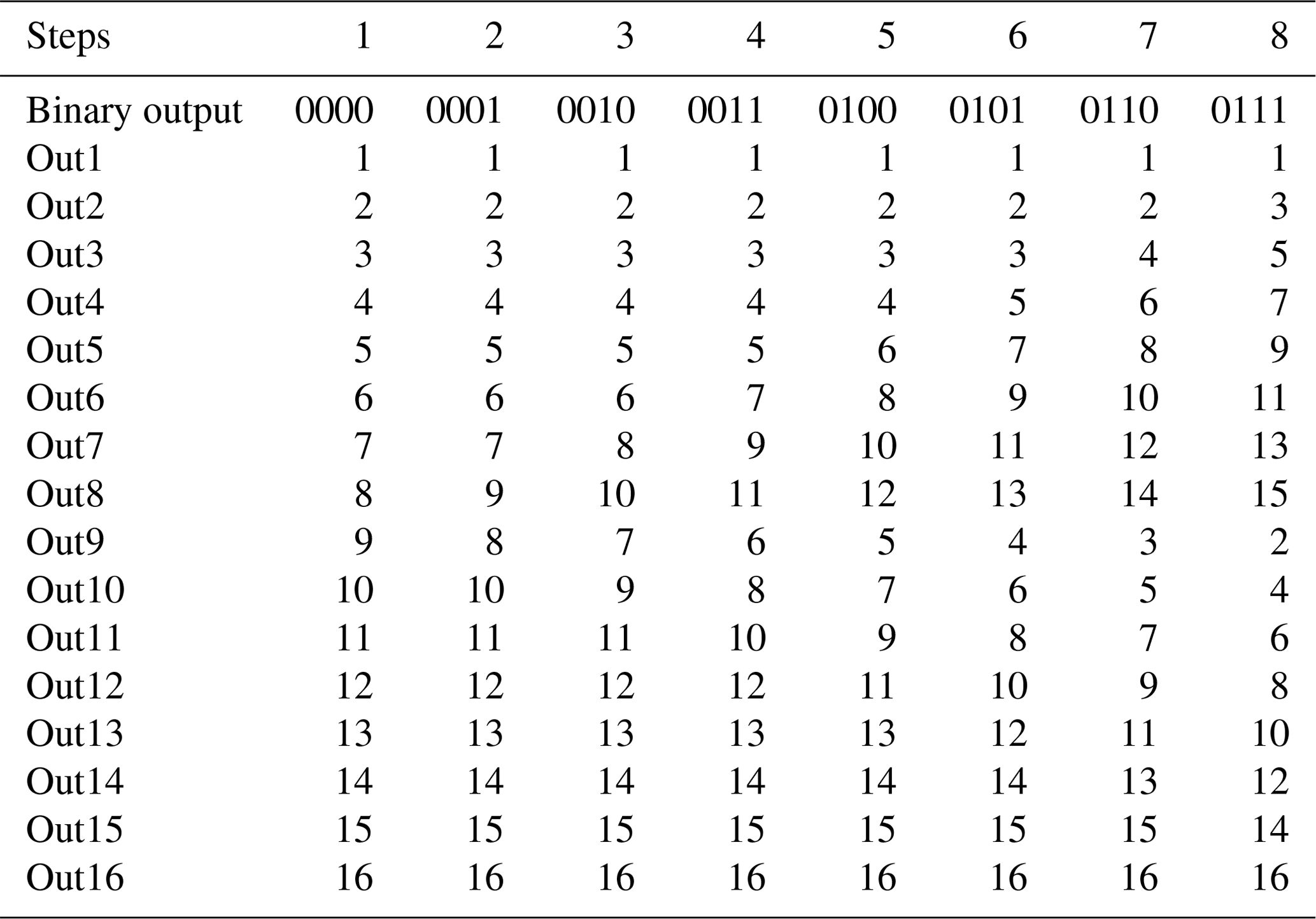
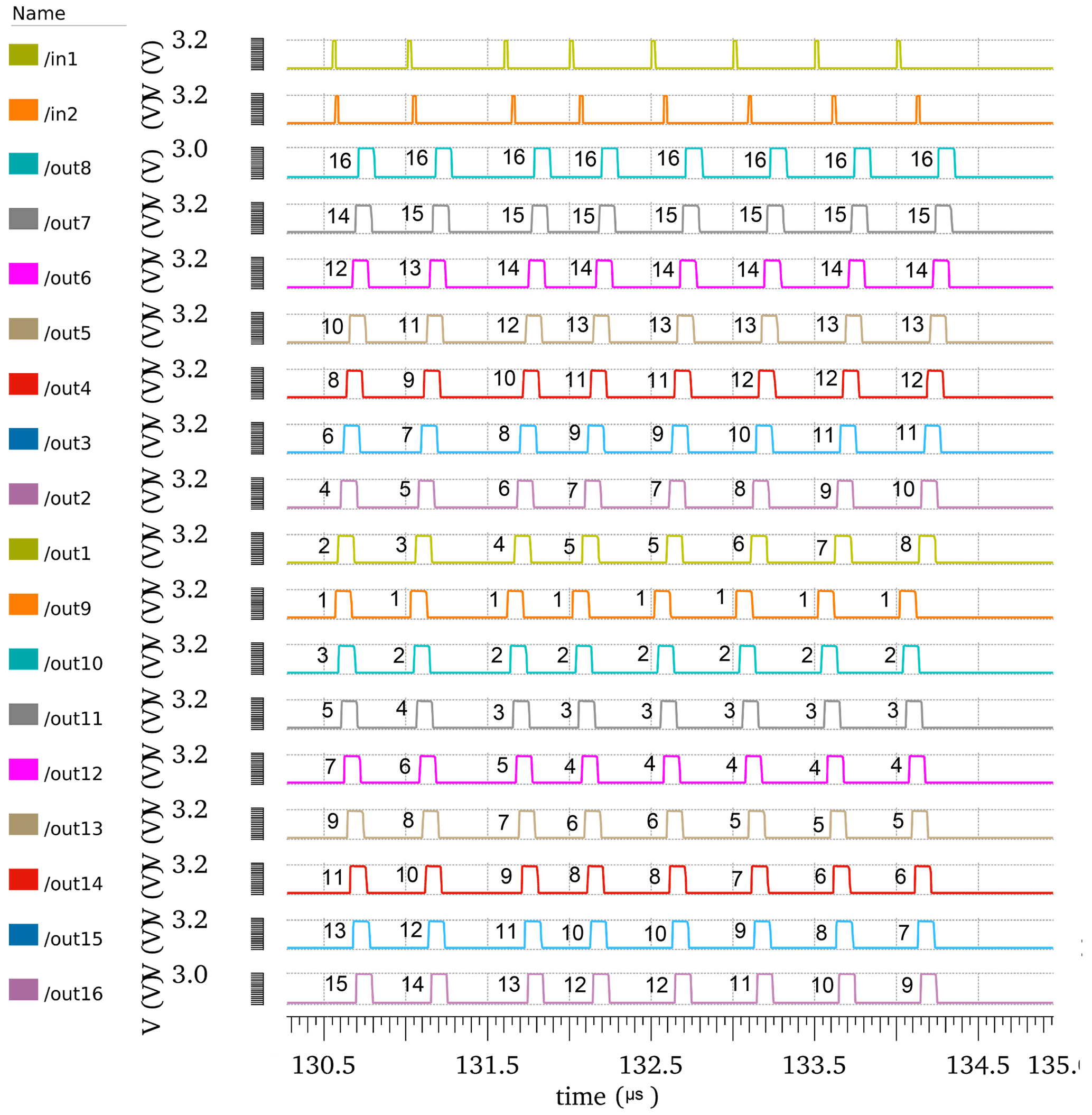
Figure 15The simulation of ASRC rank coding, with in1 preceding in2 for corner no. 2 in Table 3 at circuit conditions, where Vdd is 3.6 V, temperature is −40 ∘C, and the process corner is the WO (worst-case one). It shows that the spike order codes vary with PVT.
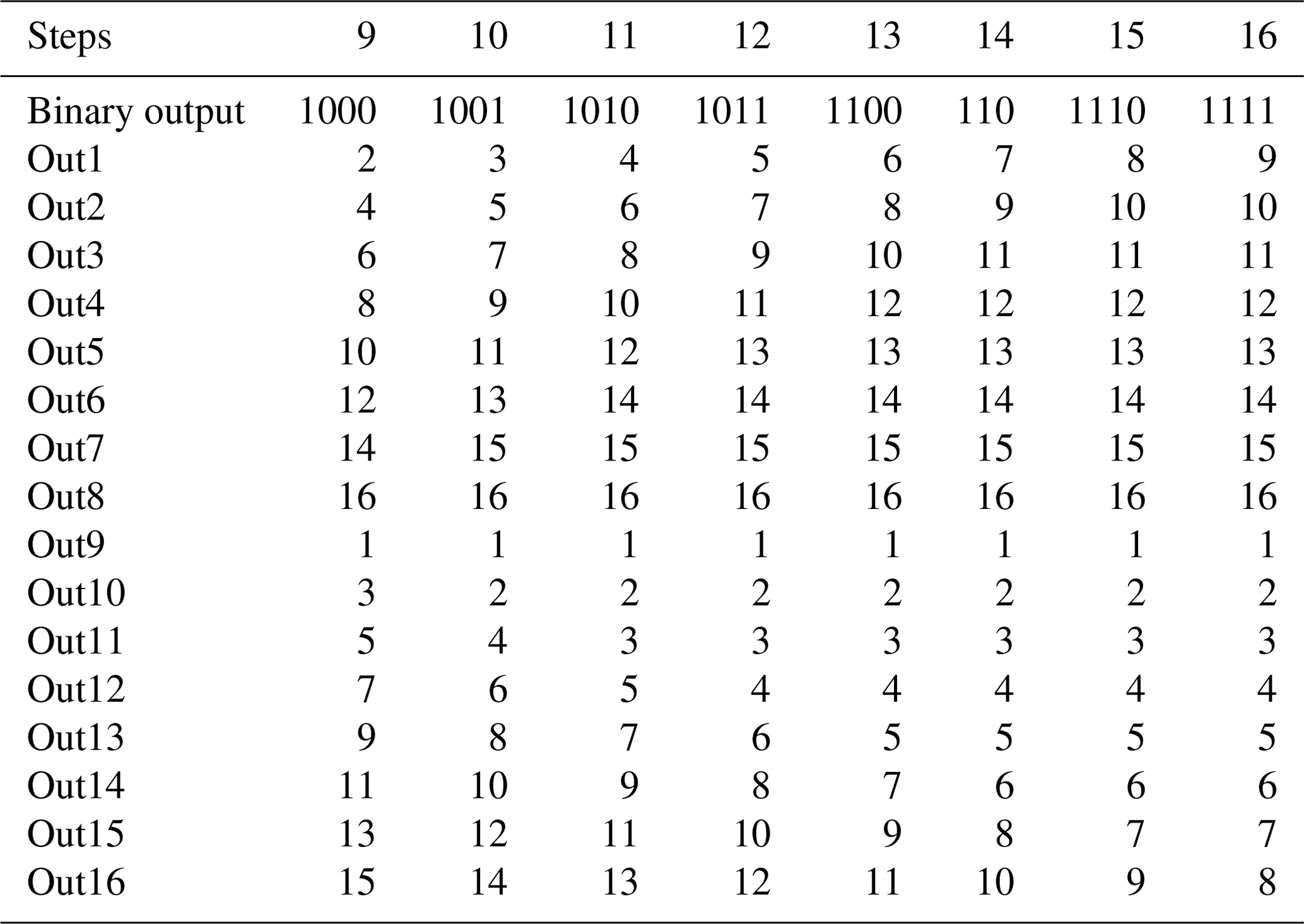
Table 3The performance of ASRC under worst-case process corners, where Tmin is −40 ∘C, Tmax is +85 ∘C, VDD(typ) is 3.3 V, VDD(min) is −10 % VDD(typ), and VDD(max) is +10 % VDD(typ). WS is the worst-case speed, WP is the worst-case power, WZ is the worst-case zero, and WO is the worst-case one.

The implemented ASRC realizes up to 16 different output spike orders, as illustrated in Tables 1 and 2. It represents 4 bits in the binary code, with a sample rate of 2.85 × 10⁶ samples per second. The operational capability of the ASRC under static and dynamic variations is proved by simulation-based validation under extreme process, voltage, and temperature (PVT) corners determined by the used X-FAB technology in this paper (Technology Xfab, 2022). The orders of the output spikes vary with PVT, as shown in Fig. 15. Figure 15 shows the simulation of ASRC rank coding, with in1 preceding in2 for corner no. 2 in Table 3. It shows that the spike order codes vary with PVT, where four output spikes orders have been changed. Figure 15 shows the change in one possible corner, and other corners are listed in Table 3 for generalization. By adapting the variables vg1, vg2, VLEAK, and VRFR, shown in Table 3, together with running the automatic adaptation of the first layer, the deviations are compensated for in every corner, where the adaptation tunes the time of neuron fire in the range between 2.3 and 9.3 ns and a resolution of 0.027 ns. The output spike orders reset to their original statuses, as shown in Fig. 14. The capability of measuring time intervals between in1 and in2 is raised by cascading more ACDs. Every ACD adds 15 ns to the delay chain and represents the least significant bit (LSB). Therefore, a corresponding number of ACDs is required to measure a maximum time interval (Tmax).
Therefore from Eqs. (1) and (2), we determine the following:
The number of bits (NOB) is computed as follows:
The time difference between the two input spikes of ASRC is changed from 120 to −120 ns for the current design. Figure 16 shows the transfer function of our SN-ADC, where the vertical axis represents the output of SN-ADC, and the horizontal axis represents the time difference between in2 and in1. There is an equivalent binary code at the SN-ADC output for each time interval in the SN-ADC input. The ideal step width of the SN-ADC should be 1 LSB. The variance in the step width between the ideal and the actual value is defined as the differential non-linearity (DNL) error. The integral non-linearity (INL) is the maximum deviation of the actual curve from the ideal curve (Henzler, 2010b). We slowly changed the time difference between in1 and in2 by a step of 0.01 LSB (0.15 ns) to measure the DNL. Figure 16 shows the transfer function of our SN-ADC under corner case no. 5 in Table 3. It has 10 steps; therefore, there are six missing codes (number of missing codes – NOMCs). The DNL and INL are 0.88 and 4 LSB, respectively, as illustrated in Fig. 16. By adapting the variables vg1, vg2, VLEAK, and VRFR, as shown in corner no. 5 in Table 3, together with running the automatic adaptation of the first layer, the deviations are compensated, as shown in Fig. 17. After adaptation, the SN-ADC parameters NOMC, DNL, and INL are no missing code (Henzler, 2010b), i.e., 0.22 and 0.4 LSB, respectively, as shown in Table 4. The simulation test is performed for the remaining corners given in Table 3.

Figure 16The transfer function of SN-ADC for both ideal and before adaptation at corner no. 5 in Table 3, at the following circuit conditions: Vdd is 3 V, temperature is 85 ∘C, and the process corner is the WO (worst-case one). Before adaptation, the SN-ADC parameters NOMC, DNL, and INL are six missing codes, i.e., 0.88 and 4 LSB, respectively.
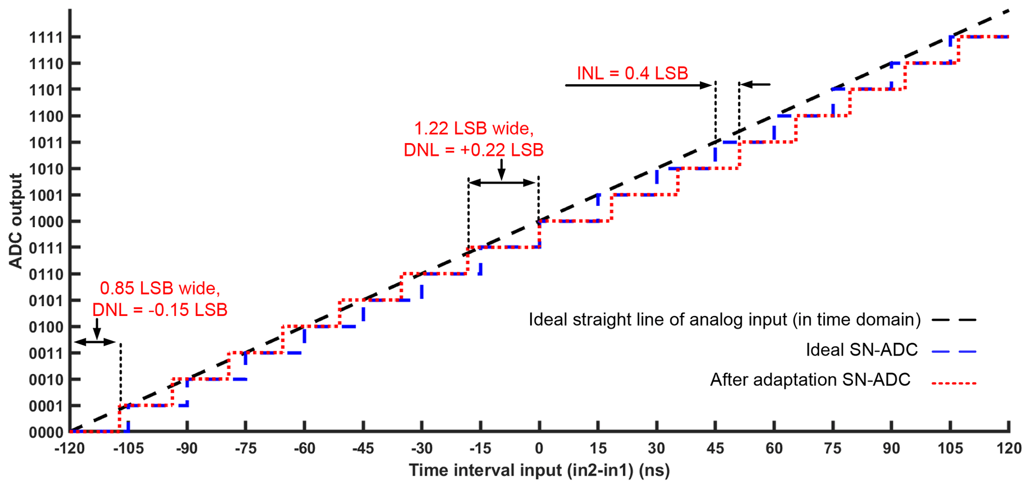
Figure 17The transfer function of SN-ADC for both ideal and after adaptation at corner no. 5 in Table 3, at the following circuit conditions: Vdd is 3 V, temperature is 85 ∘C, and the process corner is the WO (worst-case one). After adaptation, the SN-ADC parameters NOMC, DNL, and INL are no missing code, i.e., 0.22 and 0.4 LSB, respectively.
Table 4The parameter values of SN-ADC before and after adaptation.
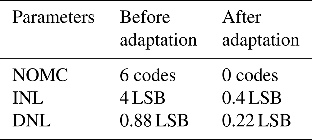
Table 5The achieved and targeted values of the synapses weight when the variables VLEAK, VRFR, vg1, and vg2 of the second layer are fixed to 700 mV, 800 mV, 1.8 V, and 220 mV, respectively.
4.5 Adaptation time
Due to the hardware restrictions of our previous paper, which presents a first-cut and not-too-practical solution, we used an up–down counter to control the weight of the synapse, and the ACDs did not connect in parallel for the adaptation. We started searching for the synapse weight from zero (for the up-counter) or maximum (for the down-counter) until we reached the target weight.
The theoretical value of the maximum adaptation time is equal to half the number of ACDs.
, where N is the number of bits of the variables, X is the number of variables, and 0.5 represents half the number of the counter steps because of the up–down counter. The adaptation time for 4 bit was 15:27 h, and the number of ACDs increases with the number of bits, as shown in Eq. (4). Therefore, the adaptation time will become infeasible for 12 bits of a practical state-of-the-art ADC, for example.
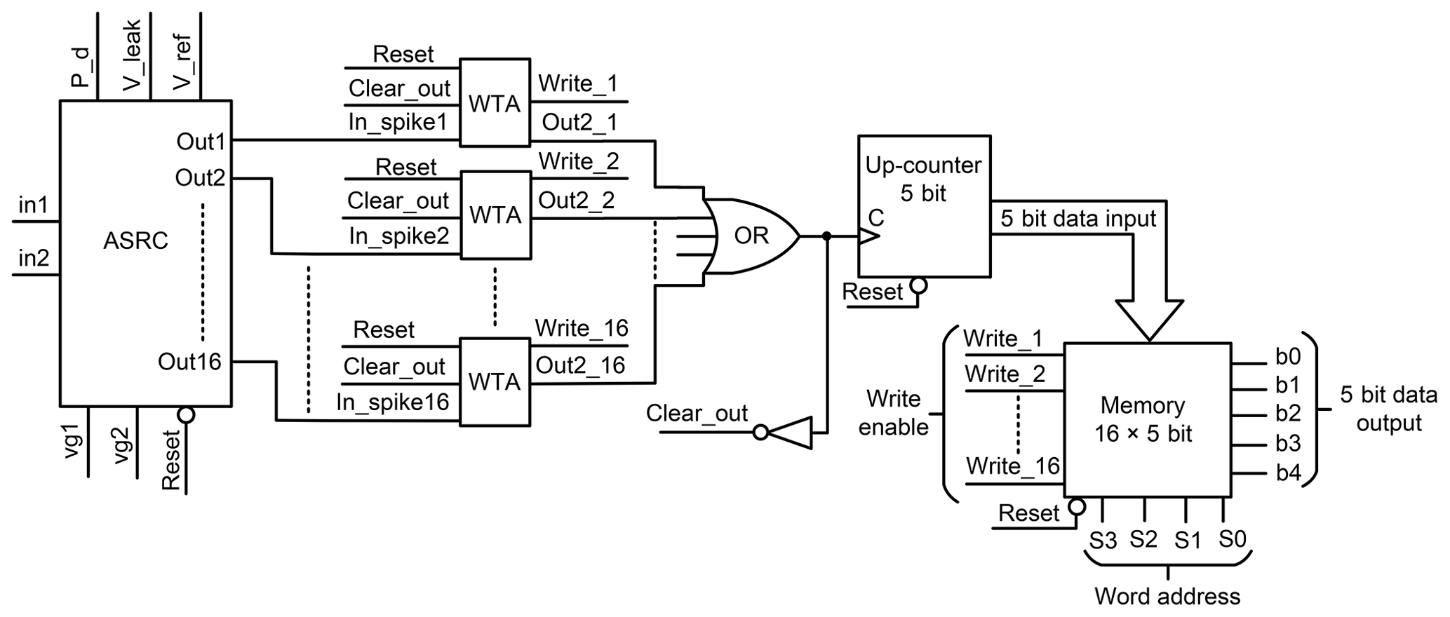
Figure 18Proposed ASDC and memory. The ASDC block generates a digital code and saves it in the memory, based on the time difference between the spikes on its inputs. Every output of ASRC is connected to a single cell of the winner-take-all (WTA) circuit. There is a position in the memory for every cell of the WTA to save its order among the other ASRC outputs.
In this work, we have two layers of the adaptation. In the first layer, the adaptation time is limited by the state's synapse weight and the input pulse frequency. The weight is adapted by the input pulse with a frequency of 5 MHz. The first synapse of all ACDs is adapted simultaneously; therefore, the adaptation time of all first synapses is 256 multiplied by 0.2 µs, which equals 51.2 µs. Equally, the second synapses take the same adaptation time. As a result, the theoretical value of the maximum adaptation time of all synapses is 102.4 µs so that, depending on the present perturbation of the regarded corner, the value can be much less than 102.4 µs. The mean value over the 3σ corner process variation is 34.8 µs, and the maximum is 77.2 µs. The adaptation time will not increase with the synapse number because all the synapses are adapted simultaneously. Consequently, every change in the variables VLEAK, VRFR, vg1, and vg2 has to wait for 102.4 µs to make the following change. The theoretical value of the maximum adaptation time of our proposed scheme is .
Each variable, VLEAK, VRFR, vg1, and vg2, has sizes of 5 bits. Therefore, the theoretical value of the maximum adaptation time of our proposed scheme is as follows:
However, this time will not increase with the number of ACDs. Therefore, for 12 bits, the adaptation time will remain the same.
The output of the ASRC is sparse rank coded spikes. An ADC chip would need a lot of output pins to read the output of the ASRC. The current design of the ASRC has 16 outputs. It is possible to readout from the chip. However, 8 bits and more ADC would have 2number of bits outputs, which is more than feasible for a simple chip. Häfliger and Aasebø (2004) presented an electronic circuit that encodes an array of input spikes into a digital number. They performed the rank order encoder by cascaded columns timing the WTA circuits. However, that scheme consumes a massive area.
Kammara and König (2016) have designed a circuit that converts the rank order code to digital numbers by one column in the WTA circuit. It consumes a much smaller area in comparison with the design in Häfliger and Aasebø (2004). They used a mechanism to determine one spike after the other by repeated sensor readout. Kammara and König (2016) assumed that the sensor output did not change. However, this structure requires many measurements to take out the rank codes.
In this work, we design a circuit that converts the rank order code to digital numbers by one column of the WTA circuit without repeating sensor readout, as shown in Fig. 18. The design in Häfliger and Aasebø (2004) used 7965 transistors for 16 inputs, while in our work, we used only 352 transistors for 16 inputs.
Every output of ASRC is connected to a single cell in the WTA circuit. There is a position in the memory for every cell of the WTA to save its order among the other ASRC outputs. The schematic of the WTA is shown in Fig. 19. The write outputs of the WTA cells are connected to the memory. They write the counter output on their position on the memory when they change from zero to one.
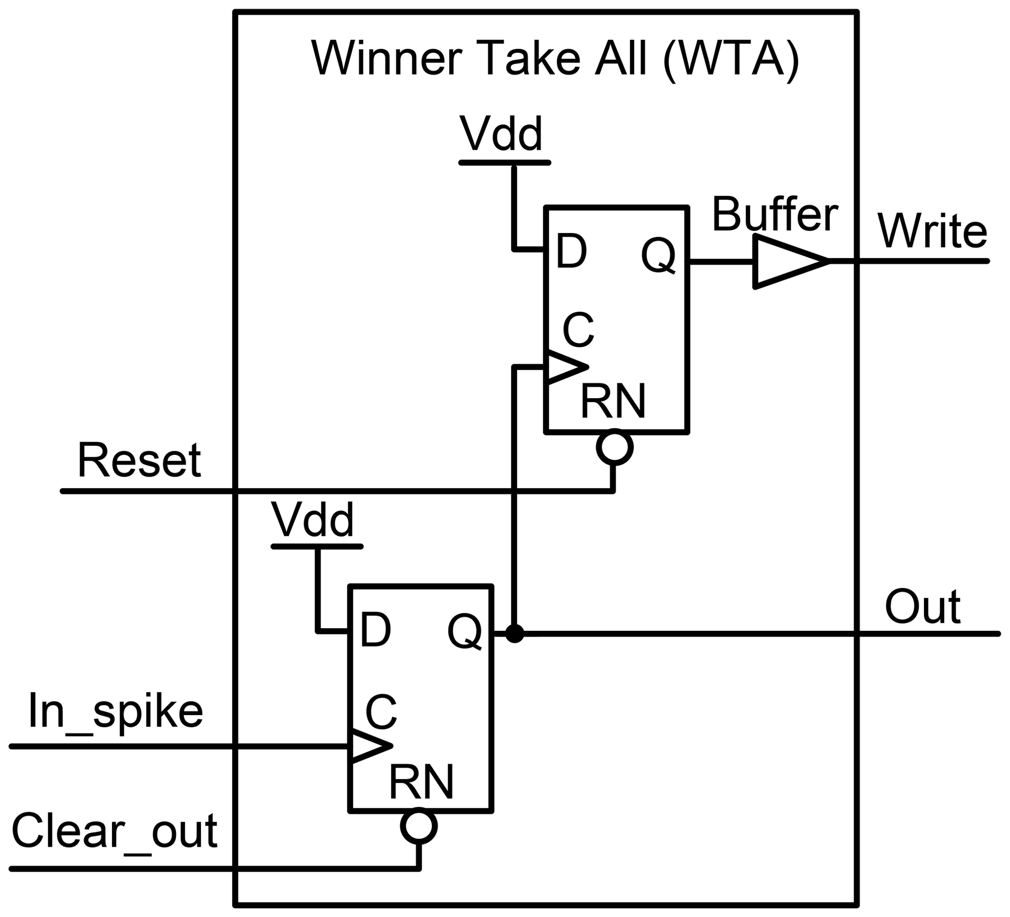
Figure 19The schematic of the winner-take-all (WTA). It is used to determine the winner among the ASRC outputs.
The current design of the ASRC has 16 outputs. Therefore, we have designed memory with the 16 address words, as shown in Fig. 20. Every address is located for one output of the ASRC to save its order. The decoder is used to select the address memory to read it. The inputs, Write_1 to Write_16, are used to write on the memory, and they are connected to the WTA cell write outputs (Write_1 to Write_16), respectively. It is written on the address when its input (Write_1 to Write_16) changes from zero to one.
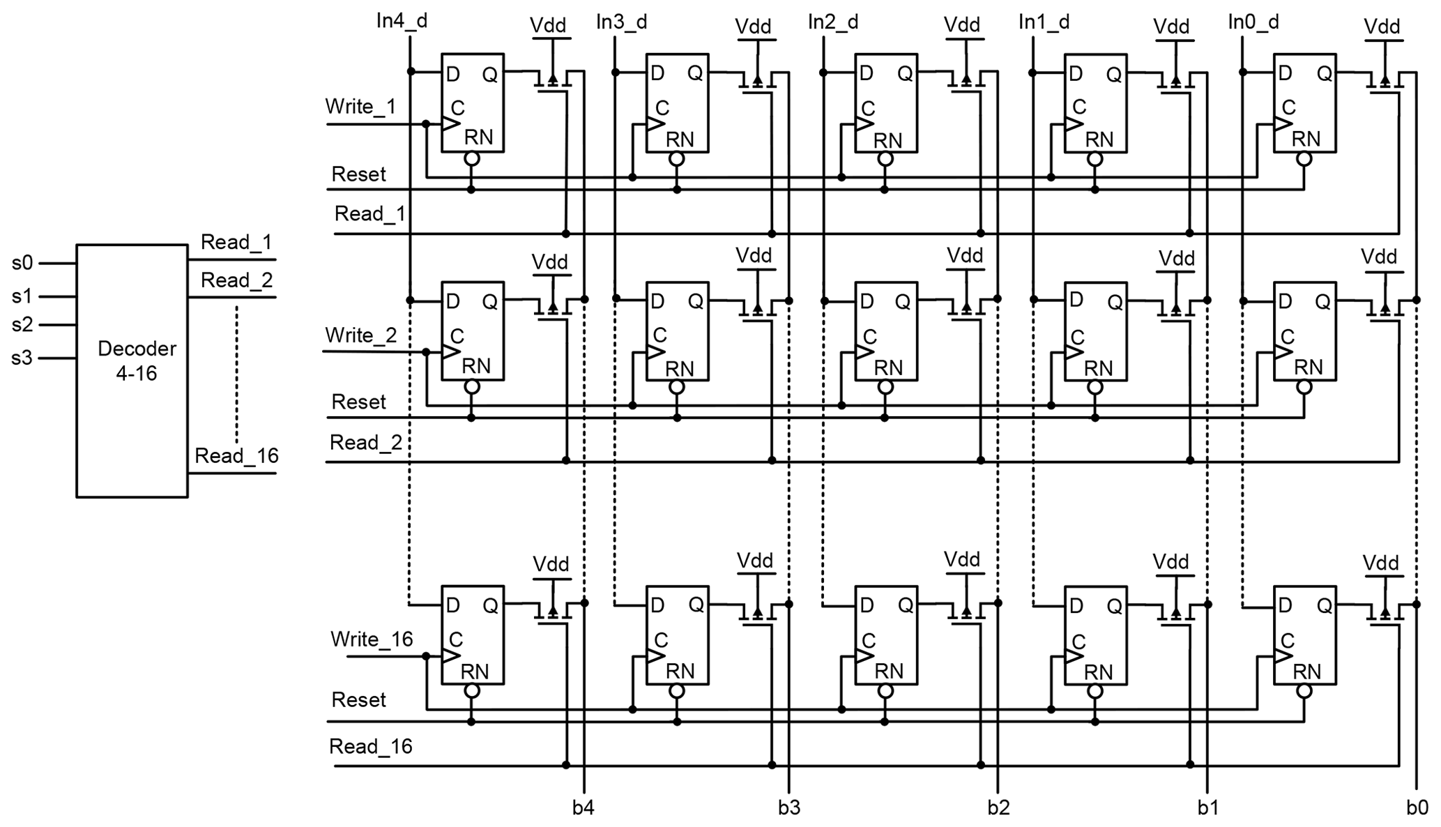
Figure 20Schematic of the memory. It is used to save the order of the ASRC outputs. The decoder is used to select the word address.
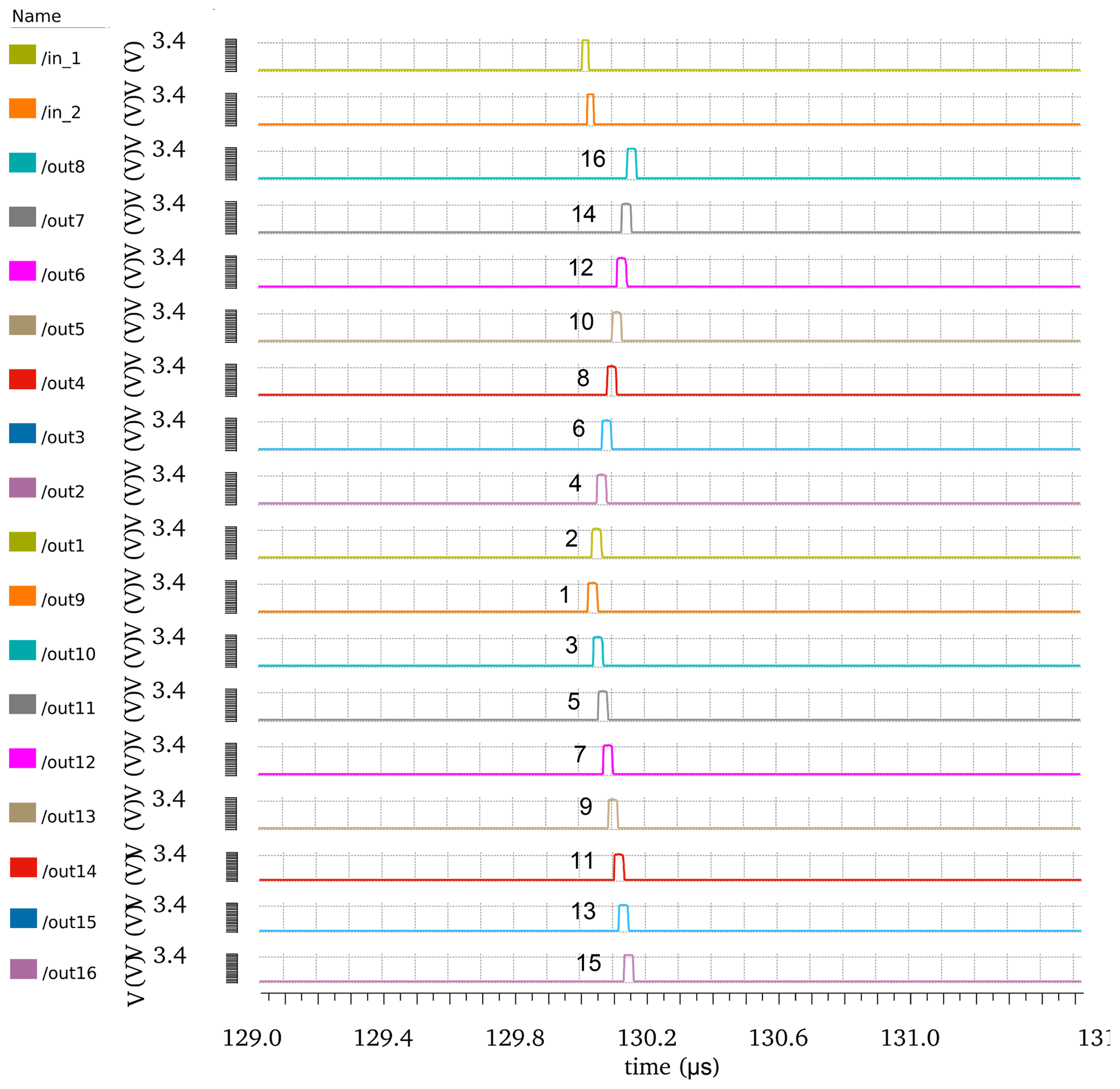
Figure 21Simulation of the ASRC, with a difference of 15 ns between in1 and in2. They are coded by spike order codes.
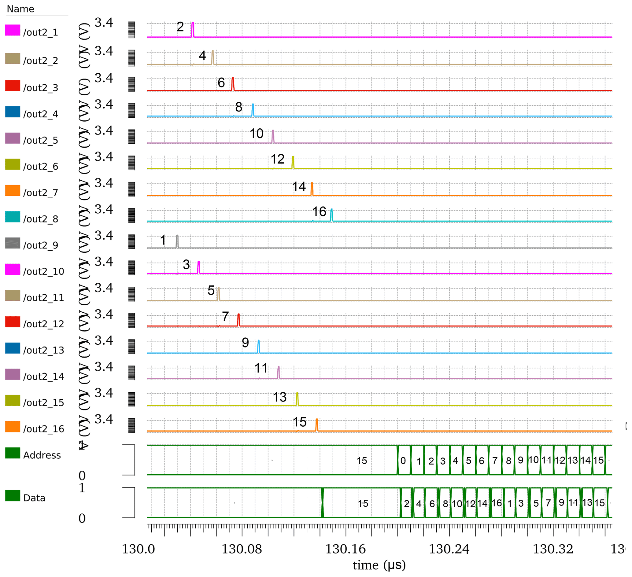
Figure 22Simulation of the WTA and memory. The terms out2_1 to out2_16 represent the outputs of the WTA cells. The decoder changes the address of the memory. The data represent the order of the outputs of the WTA cells, which are saved in the memory.
All the outputs of the WTA cells are combined by an OR gate, as shown in Fig. 18. The output of the OR gate is connected to the clock of the counter. The counter increases by one when the output of the OR gate changes from zero to one. The WTA cells determine the winner among the ASRC outputs. The first WTA cell that receives a spike on its input (In_spike) declares itself the first winner. It passes the Vdd to its output. This brings the output of the OR gate to one and increases the counter from zero to one. Also, it brings its write output to one, and this writes the output of the counter (in this case, one) on its position on the memory, representing its order among other ASRC outputs.
The buffer on the write output of the WTA circuit is used to delay the counter output reading. It makes sure that the counter was changed to a new value before reading it (in this case, from zero to one). The OR gate output is sent back through the inverter to the WTA cell input Clear_out, which reset their outputs and brings the output of the OR gate back to zero, making them ready to check the second winner. Sequentially, the cell that receives a spike declares itself the second winner. It also changes its output to one. This brings the write output and the output of the OR gate to one. Also, it changes the counter output from one to two and saves its value on its memory (in this case, two).

Figure 23Simulation of the WTA and memory at 85 ∘C. The terms out2_1 to the out2_16 represent the outputs of the WTA cells. The decoder changes the address of the memory. The data represent the order of the outputs of the WTA cells, which are saved in the memory.
The circuit shown in Fig. 18 has the capability of distinguishing between the spikes that happen with a time difference of at least 3 ns. If two WTA cells are clocking the OR gate at the same time, or less than 3 ns, then one of them will have the wrong order among other ASRC outputs. In this case, the adaptation variables vg1, vg2, VLEAK, and VRFR are adapted to compensate for the deviation to recover the time difference between the ASRC outputs spikes to more than, or equal to, 3 ns.
Figure 21 shows the outputs spike orders of the ASRC when two pulses are applied to the inputs of the ASRC in1 and in2 with a different time of 15 ns.
The ASRC outputs from out1 to out16 shown in Fig. 21 go to the WTA cells inputs from In_spike1 to In_spike16, respectively, as shown in Fig. 18. The WTA cells produce pulses with the same orders as the ASRC output orders, as shown in Fig. 22. These orders are saved on the memory. The data on the memory are read by changing the word address, as shown in Fig. 22. The word addresses from 0 to 15 are located for Out1 to Out16, respectively. For example, the word address 0 is located for Out1, and it saved its order, in this case, as 2. The word address 1 is located for Out2, and it saved its order, in this case, as 4, as shown in Fig. 22.
The circuit in Fig. 18 is tested under a temperature of 85 ∘C by applying two pulses on the in1 and in2, with a time difference of 15 ns. Also, the ASRC produces output spikes with similar orders, as shown in Fig. 21. In addition, the output orders of the WTA cells are shown in Fig. 23. They have different orders from Fig. 22, although their inputs have the same orders. This happens because the time difference between Out6 and Out15 of the ASRC becomes less than 3 ns at 85 ∘C. The WTA Out2_6 changes the OR gate's output from zero to one, and this output goes back through the inverter to reset the outputs of all WTA cells. It needs 3 ns to finish the reset process. Also, since the WTA Out2_15 comes during the process, this output does not generate a pulse to increase the counter, and the counter is increased by the following winner (Out2_7). Also, since the Write_15 output of the WTA cell remains zero, its word address remains zero too, as shown in Fig. 23.
The adaptation variables vg1, vg2, VLEAK, and VRFR are adapted to compensate for the deviation that backs the time difference between the ASRC outputs spikes to more than 3 ns. They reset the output spike orders of the WTA cells to their original orders, as shown in Fig. 22.
We have used the algorithm in Fig. 24 to decode the rank codes in Figs. 13 and 14 to binary codes.
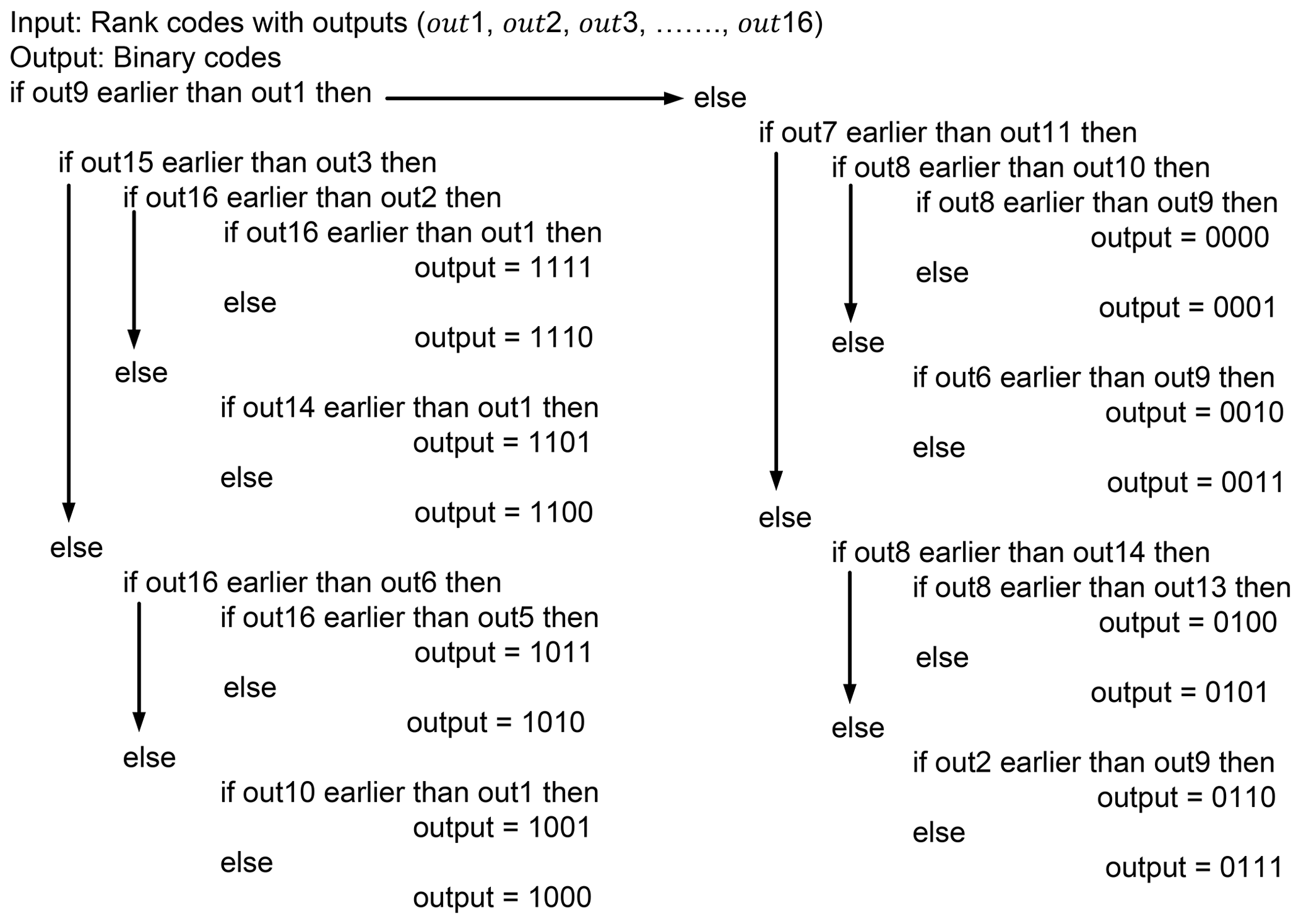
Figure 24Algorithm for decoding rank codes. It is used to decode the rank codes to binary codes.
Figure 25This graph shows the error between the desired and the actual value of the first synapse of the first ACD. The variables VLEAK, VRFR, vg1, and vg2 of the second layer are fixed to 700 mV, 800 mV, 1.8 V, and 220 mV, respectively. Circuit conditions are Vdd of 3.3 V, and temperature equals 27 ∘C and on the nominal process.

Figure 26The synaptic weight behavior LTP at vg1 equals 0 V, which is achieved by 256 input pulses applied to the 8 bit counter, whose outputs control the 8 bit binary digitized transistor of the synapse. Circuit conditions are Vdd of 3.3 V, and temperature equals 27 ∘C and on the nominal process. The vg2 has a same influence on the second synapse of ACD.
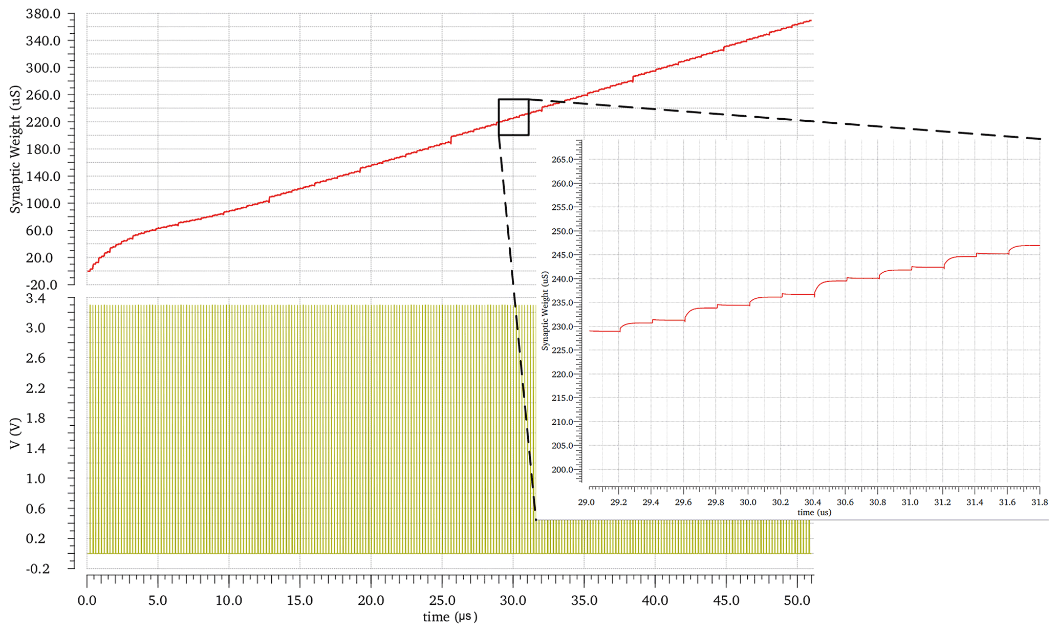
Figure 27The synaptic weight behavior LTP at vg1 equals 500 mV, which is achieved by 256 input pulses applied to the 8 bit counter, whose outputs control the 8 bit binary digitized transistor of the synapse. Circuit conditions are Vdd of 3.3 V, and temperature equals 27 ∘C and on the nominal process. The vg2 has a same influence on the second synapse of ACD.
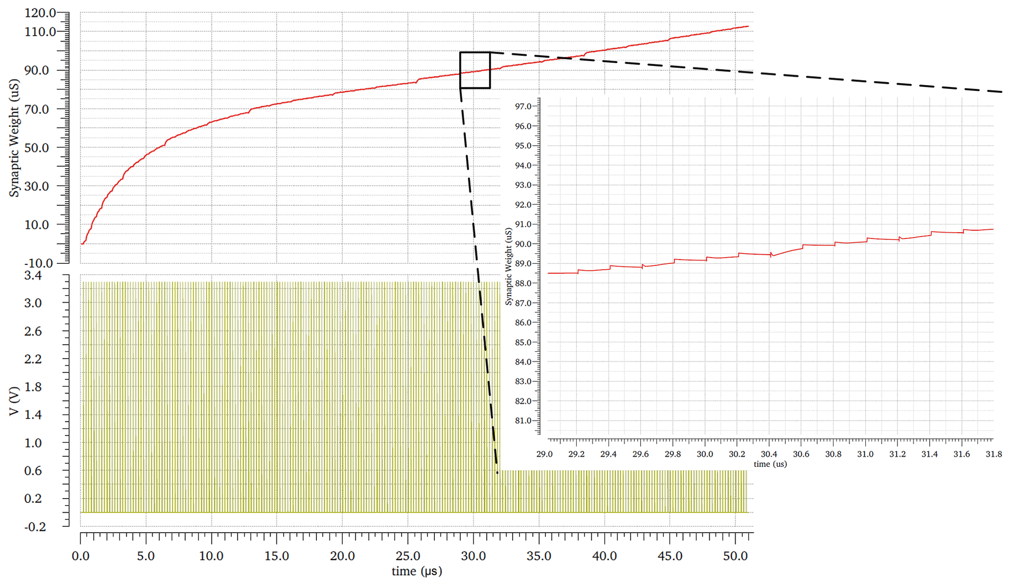
Figure 28The synaptic weight behavior LTP at vg1 equals 1 V, which is achieved by 256 input pulses applied to the 8 bit counter, whose outputs control the 8 bit binary digitized transistor of the synapse. Circuit conditions are Vdd of 3.3 V, and temperature equals 27 ∘C and on the nominal process. The vg2 has a same influence on the second synapse of ACD.
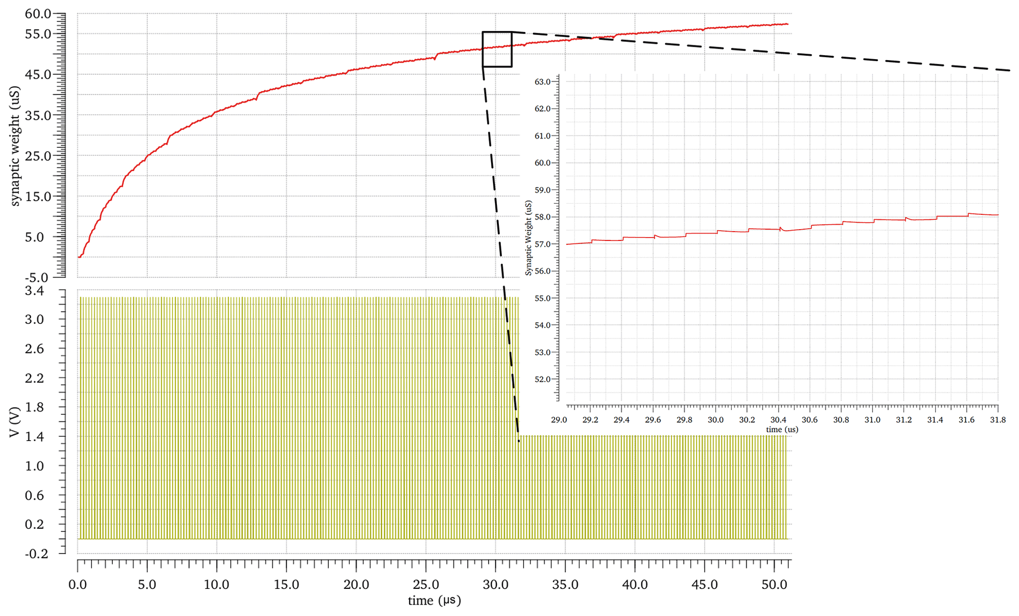
Figure 29The synaptic weight behavior LTP at vg1 equals 1.5 V, which is achieved by 256 input pulses applied to the 8 bit counter, whose outputs control the 8 bit binary digitized transistor of the synapse. Circuit conditions are Vdd of 3.3 V, and temperature equals 27 ∘C and on the nominal process. The vg2 has a same influence on the second synapse of ACD.
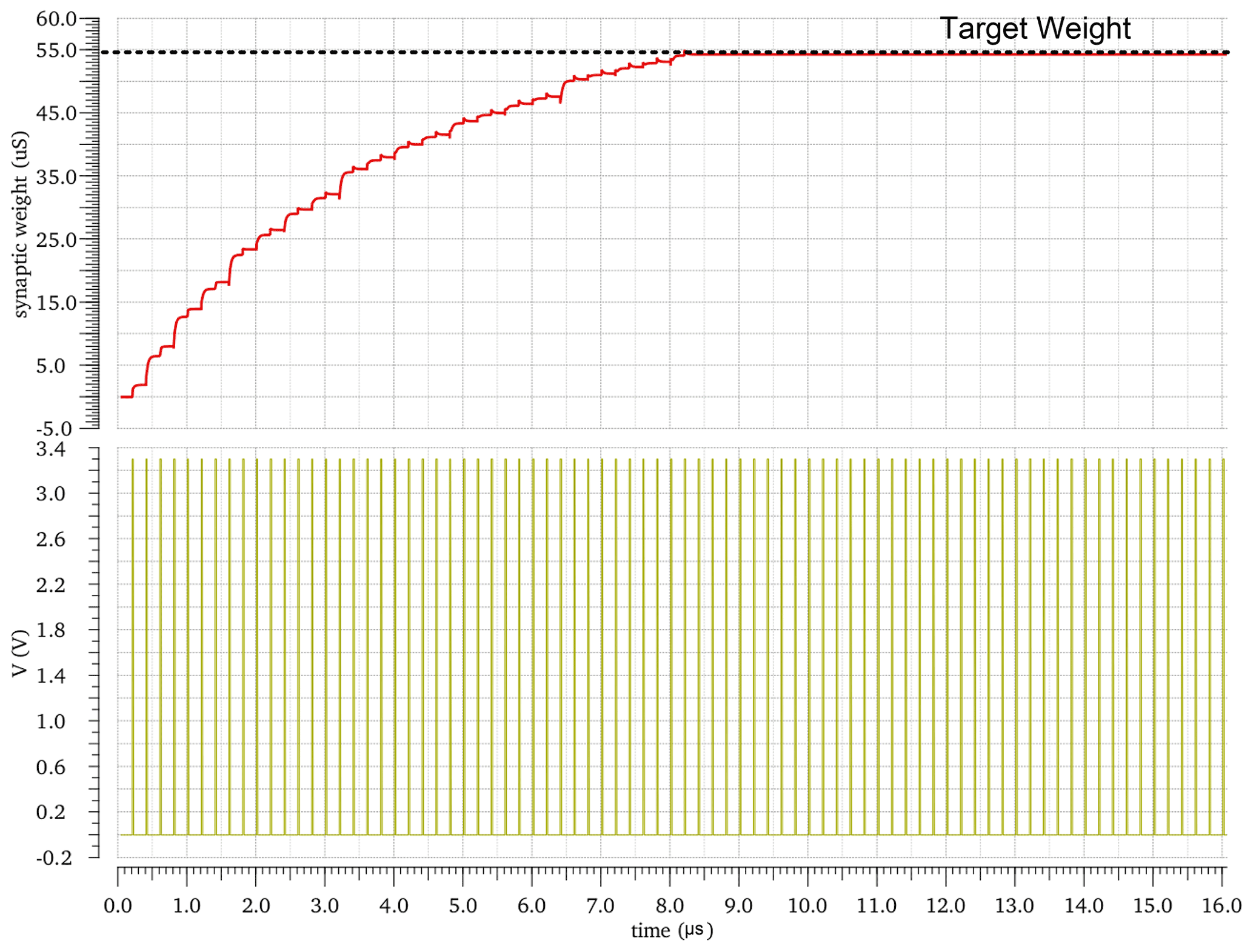
Figure 30Target weight at VRFR equal to 600 mV, vg1 and vg2 equal to 1 V, and VLEAK equal to 700 mV. Circuit conditions are Vdd of 3.3 V, and temperature equals 27 ∘C and on the nominal process.
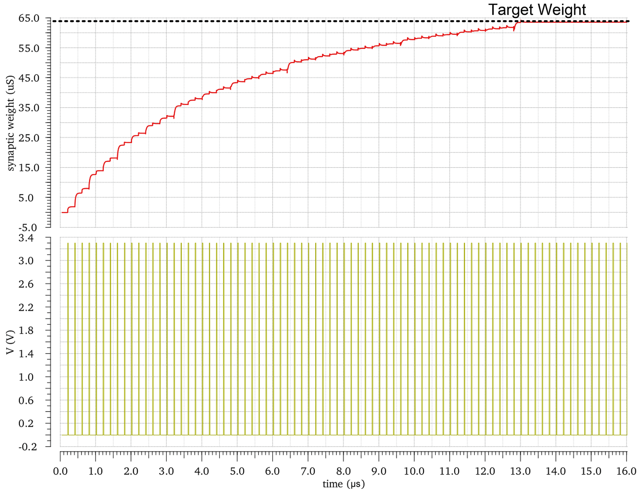
Figure 31Target weight at VRFR equal to 800 mV, vg1 and vg2 equal to 1 V, and VLEAK equal to 700 mV. Circuit conditions are Vdd of 3.3 V, and temperature equals 27 ∘C and on the nominal process.
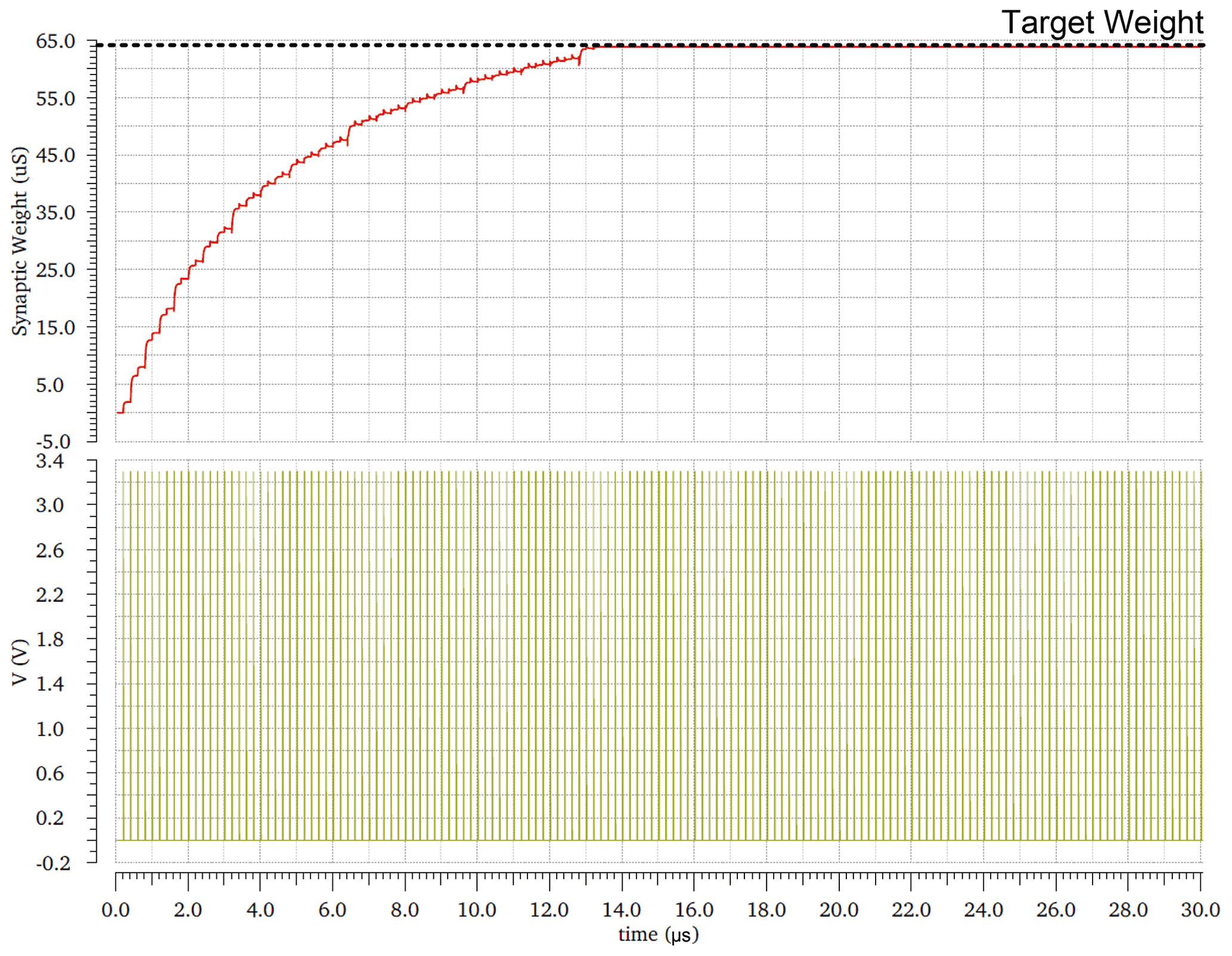
Figure 32Target weight at VLEAK equal to 500 mV, vg1 and vg2 equal to 1 V, and VRFR equal to 800 mV. Circuit conditions are Vdd of 3.3 V, and temperature equals 27 ∘C and on the nominal process.
Figure 33Target weight at VLEAK equal to 1 V, vg1 and vg2 equal to 1 V, and VRFR equal to 800 mV. Circuit conditions are Vdd of 3.3 V, and temperature equals 27 ∘C and on the nominal process.
Figure 34Target weight at VLEAK equal to 1.5 V, vg1 and vg2 equal to 1 V, and VRFR equal to 800 mV. Circuit conditions are Vdd of 3.3 V, and temperature equals 27 ∘C and on the nominal process.
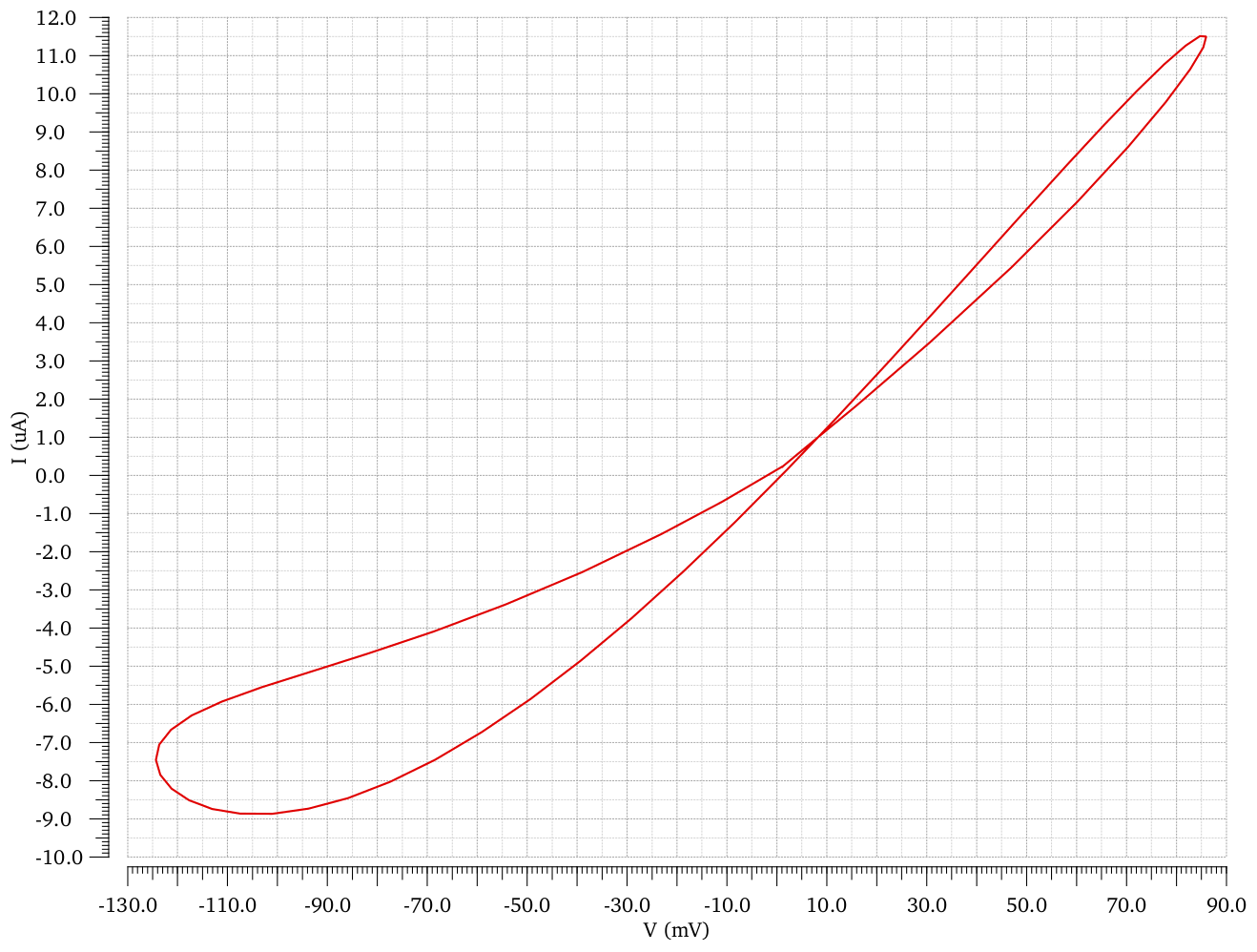
Figure 35The voltage current characteristics of the proposed memristor for 4 MHz. Circuit conditions are Vdd of 3.3 V, and temperature equals 27 ∘C and on the nominal process.
In this work, we proposed the implementation of the ASDC, which is the prime segment of the adaptive SN-ADC. The ASDC has two parts, namely the ASRC and the RBCC. A novel ACD based on a CMOS memristor is proposed to build the ASRC. We have introduced a self-adaptive method to adapt all the ACDs simultaneously. This leads to an aggressive decrease in the adaptation time of the ASRC. In contrast to the our previous implementation, the adaptation time would not be changed with the ACDs numbers where the maximum adaptation time is 107.3 s.
We have built the SN-ADC with two layers of the adaptation hierarchy. The first layer of the adaptation hierarchy is designed and presented in this work. In this layer, the adaptation circuit automatically adapts the synapses' weight and reduces the optimization problem to only four variables. Those four variables in the current stage of development of our design have been adapted manually as a second layer of the adaptation hierarchy, where the first layer depends on the second layer variables' values. Also, additional ACDs can increase the capability of measuring time intervals between in1 and in2. The number of bits for the current stage of development is 4 bits. The INL, DNL, and NOMC are 0.4 and 0.22 LSB and no missing code, respectively, from a performance parameter perspective. These parameters change with deviations, and the adaptation resets them to the best possible values. In addition, we introduced the RBCC circuit that can convert the output of the ASRC rank orders codes to the digital codes, and it has the capability of distinguishing between the spikes that happen with a time difference of 3 ns. From the energy consumption perspective, when there is no spike, the consuming energy of the ACD is 25 pJ per 1 µs; however, when there is a spike, it consumes 51 pJ per spike. On the other hand, the consuming energy of ASRC is 1.212 nJ per conversion. From the speed perspective, the conversion time is 350 ns for the ASRC. Finally, the proposed SDC is implemented utilizing X-FAB 0.35 µm CMOS technology. We plan to raise the resolution and design the remaining parts of the spiking neural SN-ADC in future work. We will develop an SSC unit which is essential for the presented work. Moreover, our future investigation intends to consider closed loops for synaptic adaptation, without bulky conventional digital components/units, to improve the next design generations by reducing sensitivities and introducing fault tolerance.
After chip fabrication, the adaptation process is mainly required to compensate for the static process variation. In contrast to costly trimming or calibration steps in the wake of the fabrication process sequentially for each separate sample chip, here, each chip self-adapts in place, i.e., all manufactured chips will adapt concurrently. Later on, the adaptation can/should be activated to cope with the dynamic variation or better drift effect, particularly the temperature drift, and aging or other sources of influence, which are usually changing on a moderate timescale and need less frequent updates. The overall sampling rate of the ADC is 2.85 MHz. After the initial static compensation by adaptation, the adaptation for dynamic effects can be executed either by interleaving continuously, with the conversion going on at its full rate but with possibly compromised accuracy, or with an interrupted or slowed down measurement interleaving with a repeated complete adaptation in one go. A tradeoff of the sampling rate and accuracy is possible by this adaptive spiking sensor electronics concept. In future work, we will extend the adaptation concept to a completely automated adaptation and conceive a physical implementation of the proposed adaptive spiking ADC to validate the simulation results by measurements.
The underlying data and coding are not publicly available because of a license agreement and data software protection of the Cadence Environment and technology from X-FAB provided under the umbrella of EUROPRACTICE.
HA was responsible for the circuit design and implementation and verification of the circuits, adaptation, and algorithm. AK contributed the SN-ADC concepts, suggestions for adaptation, design, and system verification, reference recommendations, paper structuring, paper editing, and supervising the project overall.
The contact author has declared that neither of the authors has any competing interests.
Publisher's note: Copernicus Publications remains neutral with regard to jurisdictional claims in published maps and institutional affiliations.
This article is part of the special issue “Sensors and Measurement Science International SMSI 2021”. It is a result of the Sensor and Measurement Science International, 3–6 May 2021.
The authors would like to acknowledge the Deutscher Akademischer Austauschdienst (DAAD), for sponsoring the doctoral student. We would also thank EUROPRACTICE, for their support in providing design tools, and MPW fabrication services, for our prototype chip and research activity.
This paper was edited by Marco Jose da Silva and reviewed by two anonymous referees.
Aamir, S. A., Stradmann, Y., Müller, P., Pehle, C., Hartel, A., Grübl, A., Schemmel, J., and Meier, K.: An accelerated lif neuronal network array for a large-scale mixed-signal neuromorphic architecture, IEEE T. Circuit. Syst. I, 65, 4299–4312, 2018. a
Abd, H. and König, A.: A Compact Four Transistor CMOS-Design of a Floating Memristor for Adaptive Spiking Neural Networks and Corresponding Self-X Sensor Electronics to Industry 4.0, tm-Technisches Messen, 87, s91–s96, 2020. a
Abd, H. and König, A.: Adaptive Spiking Sensor System Based on CMOS Memristors Emulating Long and Short-Term Plasticity of Biological Synapses for Industry 4.0 Applications, tm-Technisches Messen, 88, s114–s119, 2021a. a
Abd, H. and König, A.: D10.3 Adaptive Spiking Sensor Electronics Inspired by Biological Nervous System Based on Memristor Emulator for Industry 4.0 Applications, SMSI 2021-Sensors and Instrumentation, 232–233, https://doi.org/10.5162/SMSI2021/D10.3, 2021b. a
Alraho, S., Zaman, Q., and König, A.: Reconfigurable Wide Input Range, Fully-Differential Indirect Current-Feedback Instrumentation Amplifier with Digital Offset Calibration for Self-X Measurement Systems, tm-Technisches Messen, 87, s85–s90, 2020. a, b
Ashida, G. and Carr, C. E.: Sound localization: Jeffress and beyond, Curr. Opin. Neurobiol., 21, 745–751, 2011. a, b
Babacan, Y., Yesil, A., and Kacar, F.: Memristor emulator with tunable characteristic and its experimental results, AEU-Int. J. Electron. Commun., 81, 99–104, 2017. a, b
Berdan, R., Vasilaki, E., Khiat, A., Indiveri, G., Serb, A., and Prodromakis, T.: Emulating short-term synaptic dynamics with memristive devices, Sci. Rep., 6, 1–9, 2016. a, b
Burr, G. W., Shelby, R. M., Sebastian, A., Kim, S., Kim, S., Sidler, S., Virwani, K., Ishii, M., Narayanan, P., Fumarola, A., Sanches, L. L., Boybat, I., Gallo, M. L., Moon, K., Woo, J., Hwang, H., and Leblebici, Y.: Neuromorphic computing using non-volatile memory, Adv. Phys. X, 2, 89–124, 2017. a
Cao, H. and Wang, F.: Spreading Operation Frequency Ranges of Memristor Emulators via a New Sine-Based Method, IEEE T. VLSI Syst., 29, 617–630, 2021. a, b
Carr, C. and Konishi, M.: A circuit for detection of interaural time differences in the brain stem of the barn owl, J. Neurosci., 10, 3227–3246, 1990. a
Carr, C. E. and Christensen-Dalsgaard, J.: Sound localization strategies in three predators, Brain. Behav. Evol., 86, 17–27, 2015. a
Carr, C. E. and Konishi, M.: Axonal delay lines for time measurement in the owl's brainstem, P. Natl. Acad. Sci. USA, 85, 8311–8315, 1988. a
Covi, E., Lin, Y.-H., Wang, W., Stecconi, T., Milo, V., Bricalli, A., Ambrosi, E., Pedretti, G., Tseng, T.-Y., and Ielmini, D.: A volatile RRAM synapse for neuromorphic computing, in: 2019 26th IEEE International Conference on Electronics, Circuits and Systems (ICECS), 27 November 2019, Genoa, Italy, 903–906, https://doi.org/10.1109/ICECS46596.2019.8965044, 2019. a
Doge, J., Schonfelder, G., Streil, G. T., and Konig, A.: An HDR CMOS image sensor with spiking pixels, pixel-level ADC, and linear characteristics, IEEE T. Circuit. Syst. II, 49, 155–158, 2002. a
Graves, C. E., Li, C., Sheng, X., Miller, D., Ignowski, J., Kiyama, L., and Strachan, J. P.: In-Memory Computing with Memristor Content Addressable Memories for Pattern Matching, Adv. Mater., 32, 2003437, https://doi.org/10.1002/adma.202003437, 2020. a, b
Grothe, B., Pecka, M., and McAlpine, D.: Mechanisms of sound localization in mammals, Physiol. Rev., 90, 983–1012, 2010. a
Guo, W., Fouda, M. E., Eltawil, A. M., and Salama, K. N.: Neural coding in spiking neural networks: A comparative study for robust neuromorphic systems, Front. Neurosci., 15, 212, https://doi.org/10.3389/fnins.2021.638474, 2021. a
Häfliger, P. and Aasebø, E. J.: A rank encoder: Adaptive analog to digital conversion exploiting time domain spike signal processing, Analog Integr. Circuit. Signal Process., 40, 39–51, 2004. a, b, c
Henzler, S.: Time-to-digital converter basics, in: Time-to-digital converters, Springer, 5–18, https://doi.org/10.1007/978-90-481-8628-0_2, 2010a. a, b
Henzler, S.: Theory of tdc operation, in: Time-to-digital Converters, Springer, 19–42, https://doi.org/10.1007/978-90-481-8628-0_3, 2010b. a, b
Indiveri, G.: A low-power adaptive integrate-and-fire neuron circuit, in: vol. 4, Proceedings of the 2003 International Symposium on Circuits and Systems, ISCAS'03, 25–28 May 2003, Bangkok, Thailand https://doi.org/10.1109/ISCAS.2003.1206342, 2003. a
Jeffress, L. A.: A place theory of sound localization, J. Compar. Physiol. Psychol., 41, 35, https://doi.org/10.1037/h0061495, 1948. a, b, c, d
Jo, S.-H., Cho, H.-W., and Yoo, H.-J.: A fully reconfigurable universal sensor analog front-end IC for the internet of things era, IEEE Sensors J., 19, 2621–2633, 2019. a
Kammara, A. and König, A.: SSDCα–Inherently robust integrated biomimetic sensor-to-spike-to-digital converter based on peripheral neural ensembles, tm-Technisches Messen, 83, 531–542, 2016. a, b, c, d, e, f
Kammara, A. C. and Koenig, A.: Contributions to integrated adaptive spike coded sensor signal conditioning and digital conversion in neural architecture, in: Sensors and Measuring Systems 2014; 17. ITG/GMA Symposium, VDE, 3–4 June 2014, Nuremberg, Germany, 1–6, ISBN 978-3-8007-3622-5, 2014a. a, b
Kammara, A. C. and König, A.: P5-Increasing the Resolution of an Integrated Adaptive Spike Coded Sensor to Digital Conversion Neuro-Circuit by an Enhanced Place Coding Layer, Tagungsband, SMSI – Sensor and Measurement Science International, 157–166, https://doi.org/10.5162/AHMT2014/P5, 2014b. a, b
Kandel, E. R.: From nerve cells to cognition: The internal cellular representation required for perception and action, Princip. Neural Sci., 4, 381–403, 2000. a
Kanyal, G., Kumar, P., Paul, S. K., and Kumar, A.: OTA based high frequency tunable resistorless grounded and floating memristor emulators, AEU-Int. J. Electron. Commun., 92, 124–145, 2018. a, b
Kim, M.-K. and Lee, J.-S.: Short-term plasticity and long-term potentiation in artificial biosynapses with diffusive dynamics, ACS Nano, 12, 1680–1687, 2018a. a
Kim, M.-K. and Lee, J.-S.: Short-term plasticity and long-term potentiation in artificial biosynapses with diffusive dynamics, ACS Nano, 12, 1680–1687, 2018b. a
Kim, S., Du, C., Sheridan, P., Ma, W., Choi, S., and Lu, W. D.: Experimental demonstration of a second-order memristor and its ability to biorealistically implement synaptic plasticity, Nano Lett., 15, 2203–2211, 2015. a
Kim, S. G., Han, J. S., Kim, H., Kim, S. Y., and Jang, H. W.: Recent advances in memristive materials for artificial synapses, Adv. Mater Technol., 3, 1800457, https://doi.org/10.1002/admt.201800457, 2018. a
Kim, T., Hu, S., Kim, J., Kwak, J. Y., Park, J., Lee, S., Kim, I., Park, J.-K., and Jeong, Y.: Spiking Neural Network (SNN) with memristor synapses having non-linear weight update, Front. Comput. Neurosci., 15, 22, https://doi.org/10.3389/fncom.2021.646125, 2021. a
Koenig, A.: Integrated sensor electronics with self-x capabilities for advanced sensory systems as a baseline for industry 4.0, in: Sensors and Measuring Systems, 19th ITG/GMA-Symposium, VDE, 26–27 June 2018, Nuremberg, Germany, 1–4, ISBN 978-3-8007-4683-5, 2018. a, b
König, A. and Kammara, A. C.: B2. 1-Robust & Technology Agnostic Integrated Implementation of Future Sensory Electronics based on Spiking Information Processing for Industry 4.0, in: Proceedings Sensor 2017, 30 May–1 June 2017, Nuremberg, Germany, 177–182, https://doi.org/10.5162/sensor2017/B2.1, 2017. a, b
Krestinskaya, O., James, A. P., and Chua, L. O.: Neuromemristive circuits for edge computing: A review, IEEE T. Neural Netw. Learn. Syst., 31, 4–23, 2019. a, b
Lee, S., Shi, C., Wang, J., Sanabria, A., Osman, H., Hu, J., and Sánchez-Sinencio, E.: A built-in self-test and in situ analog circuit optimization platform, IEEE T. Circuit. Syst. I, 65, 3445–3458, 2018a. a
Lee, S., Shi, C., Wang, J., Sanabria, A., Osman, H., Hu, J., and Sánchez-Sinencio, E.: A built-in self-test and in situ analog circuit optimization platform, IEEE T. Circuit. Syst. I, 65, 3445–3458, 2018b. a
Leitch, O., Anderson, A., Kirkbride, K. P., and Lennard, C.: Biological organisms as volatile compound detectors: A review, Forensic Sci. Int., 232, 92–103, 2013. a
Li, J., Dong, Z., Luo, L., Duan, S., and Wang, L.: A novel versatile window function for memristor model with application in spiking neural network, Neurocomputing, 405, 239–246, 2020. a
Li, S., Zeng, F., Chen, C., Liu, H., Tang, G., Gao, S., Song, C., Lin, Y., Pan, F., and Guo, D.: Synaptic plasticity and learning behaviours mimicked through Ag interface movement in an Ag/conducting polymer/Ta memristive system, J. Mater. Chem. C, 1, 5292–5298, 2013. a
Lin, Y.-B., Lin, Y.-W., Lin, J.-Y., and Hung, H.-N.: SensorTalk: An IoT device failure detection and calibration mechanism for smart farming, Sensors, 19, 4788, https://doi.org/10.3390/s19214788, 2019. a
Lu, Y., Yuan, G., Der, L., Ki, W.-H., and Yue, C. P.: A ±0.5 % Precision On-Chip Frequency Reference With Programmable Switch Array for Crystal-Less Applications, IEEE T. Circuit. Syst. II, 60, 642–646, 2013. a
Lv, Z., Zhou, Y., Han, S.-T., and Roy, V.: From biomaterial-based data storage to bio-inspired artificial synapse, Mater. Today, 21, 537–552, 2018. a
Mannan, Z. I., Kim, H., and Chua, L.: Implementation of Neuro-Memristive Synapse for Long-and Short-Term Bio-Synaptic Plasticity, Sensors, 21, 644, https://doi.org/10.3390/s21020644, 2021. a
Manouras, V., Stathopoulos, S., Serb, A., and Prodromakis, T.: Technology agnostic frequency characterization methodology for memristors, Scient. Rep., 11, 1–11, 2021. a
Martin, S. J., Grimwood, P. D., and Morris, R. G.: Synaptic plasticity and memory: an evaluation of the hypothesis, Annu. Rev. Neurosci., 23, 649–711, 2000. a
Mehonic, A., Sebastian, A., Rajendran, B., Simeone, O., Vasilaki, E., and Kenyon, A. J.: Memristors – From In-Memory Computing, Deep Learning Acceleration, and Spiking Neural Networks to the Future of Neuromorphic and Bio-Inspired Computing, Adv. Intell. Syst., 2, 2000085, https://doi.org/10.1002/aisy.202000085, 2020. a
Meijer, G.: Smart sensor systems, John Wiley & Sons, ISBN 978-0-470-86691-7, 2008. a
Midya, R., Wang, Z., Asapu, S., Joshi, S., Li, Y., Zhuo, Y., Song, W., Jiang, H., Upadhay, N., Rao, M., Lin, P., Li, C., Xia, Q., and Yang, J. J.: Artificial neural network (ANN) to spiking neural network (SNN) converters based on diffusive memristors, Adv. Electron. Mater., 5, 1900060, https://doi.org/10.1002/aelm.201900060, 2019. a
Ohno, T., Hasegawa, T., Tsuruoka, T., Terabe, K., Gimzewski, J. K., and Aono, M.: Short-term plasticity and long-term potentiation mimicked in single inorganic synapses, Nat. Mater., 10, 591–595, 2011. a
Park, Y., Kim, M.-K., and Lee, J.-S.: Emerging memory devices for artificial synapses, J. Mater. Chem. C, 8, 9163–9183, 2020. a
Prasad, S. S., Kumar, P., and Ranjan, R. K.: Resistorless Memristor Emulator Using CFTA and Its Experimental Verification, IEEE Access, 9, 64065–64075, 2021. a, b
Ren, Y., Hu, L., Mao, J.-Y., Yuan, J., Zeng, Y.-J., Ruan, S., Yang, J.-Q., Zhou, L., Zhou, Y., and Han, S.-T.: Phosphorene nano-heterostructure based memristors with broadband response synaptic plasticity, J. Mater. Chem. C, 6, 9383–9393, 2018. a
Sánchez-López, C., Mendoza-Lopez, J., Carrasco-Aguilar, M., and Muñiz-Montero, C.: A floating analog memristor emulator circuit, IEEE T. Circuit. Syst. II, 61, 309–313, 2014. a, b
Seidl, A. H., Rubel, E. W., and Harris, D. M.: Mechanisms for adjusting interaural time differences to achieve binaural coincidence detection, J. Neurosci., 30, 70–80, 2010. a
Shchanikov, S., Zuev, A., Bordanov, I., Danilin, S., Lukoyanov, V., Korolev, D., Belov, A., Pigareva, Y., Gladkov, A., Pimashkin, A., Mikhaylov, A., Kazantsev, V., and Serb, A.: Designing a bidirectional, adaptive neural interface incorporating machine learning capabilities and memristor-enhanced hardware, Chaos Solit. Fract., 142, 110504, https://doi.org/10.1016/j.chaos.2020.110504, 2021. a, b
Staszewski, R. B., Wallberg, J. L., Rezeq, S., Hung, C.-M., Eliezer, O. E., Vemulapalli, S. K., Fernando, C., Maggio, K., Staszewski, R., Barton, N., Lee, M. C., Cruise, P., Entezari, M., Muhammad, K., and Leipold, D.: All-digital PLL and transmitter for mobile phones, IEEE J. Solid-State Circuit., 40, 2469–2482, 2005. a, b
Stieve, H.: Sensors of biological organisms–biological transducers, Sensors Actuat., 4, 689–704, 1983. a
Subramanyam, K. and Chandra, A.: Conception and First Implementation of Novel Sensory Signal Conditioning and Digital Conversion Electronics Based on Spiking Neuron Ensembles for Inherently Robust Processing in Aggressively Scaled Integration Technologies, Technische Universität Kaiserslautern, Kaiserslautern, https://kluedo.ub.uni-kl.de/frontdoor/index/index/docId/4774 (last access: 4 August 2022), 2017. a, b
Tavolga, W. N., Popper, A. N., and Fay, R. R.: Hearing and sound communication in fishes, Springer Science & Business Media, https://doi.org/10.1007/978-1-4615-7186-5, 2012. a
Technology Xfab: Technology X-FAB, https://www.xfab.com/technology, last access: 4 August 2022. a
Thorpe, S. and Gautrais, J.: Rank order coding, in: Computational neuroscience, Springer, 113–118, https://doi.org/10.1007/978-1-4615-4831-7_19, 1998. a
Thorpe, S., Delorme, A., and Van Rullen, R.: Spike-based strategies for rapid processing, Neural Netw., 14, 715–725, 2001. a
Von Neumann, J.: First Draft of a Report on the EDVAC, Moore School of Electrical Engineering, Univ. of Pennsylvania, Philadelphia, http://abelgo.cn/cs101/papers/Neumann.pdf (last access: 9 August 2022), 30 June 1945. a
Wang, Z., Joshi, S., Savel'ev, S. E., Jiang, H., Midya, R., Lin, P., Hu, M., Ge, N., Strachan, J. P., Li, Z., Wu, Q., Barnell, M., Li, G. L., Xin, H. L., Williams, R. S., Xia, Q., and Yang J. J.: Memristors with diffusive dynamics as synaptic emulators for neuromorphic computing, Nat. Mater., 16, 101–108, 2017. a
Werthschützky, R.: Sensor Technologien 2022, AMA Verband für Sensorik und Messtechnik eV, https://www.konstruktionspraxis.vogel.de/ama-verband-veroeffentlicht-studie-sensor-technologien-2022 (last access: 4 August 2022), 2018. a
Wu, L., Liu, H., Lin, J., and Wang, S.: Volatile and Nonvolatile Memory Operations Implemented in a Pt/HfO2/Ti Memristor, IEEE T. Elect. Devic., 68, 1622–1626, 2021. a
Yadav, N., Rai, S. K., and Pandey, R.: Novel memristor emulators using fully balanced VDBA and grounded capacitor, Iranian Journal of Science and Technology, T. Elect. Eng., 45, 229–245, 2021. a, b, c
Yang, M., Zhao, X., Tang, Q., Cui, N., Wang, Z., Tong, Y., and Liu, Y.: Stretchable and conformable synapse memristors for wearable and implantable electronics, Nanoscale, 10, 18135–18144, 2018. a
Yang, Y., Yin, M., Yu, Z., Wang, Z., Zhang, T., Cai, Y., Lu, W. D., and Huang, R.: Multifunctional Nanoionic Devices Enabling Simultaneous Heterosynaptic Plasticity and Efficient In-Memory Boolean Logic, Adv. Elect. Mater., 3, 1700032, https://doi.org/10.1002/aelm.201700032, 2017. a
Zaman, Q., Alraho, S., and König, A.: Efficient transient testing procedure using a novel experience replay particle swarm optimizer for THD-based robust design and optimization of self-X sensory electronics in industry 4.0, J. Sens. Sens. Syst., 10, 193–206, https://doi.org/10.5194/jsss-10-193-2021, 2021. a
Zhang, X., Liu, S., Zhao, X., Wu, F., Wu, Q., Wang, W., Cao, R., Fang, Y., Lv, H., Long, S., Liu, Q., and Liu, M.: Emulating short-term and long-term plasticity of bio-synapse based on Cu/a-Si/Pt memristor, IEEE Elect. Devic. Lett., 38, 1208–1211, 2017. a
Zhang, Y., Wang, Z., Zhu, J., Yang, Y., Rao, M., Song, W., Zhuo, Y., Zhang, X., Cui, M., Shen, L., Huang, R., and Yang, J.: Brain-inspired computing with memristors: Challenges in devices, circuits, and systems, Appl. Phys. Rev., 7, 011308, https://doi.org/10.1063/1.5124027, 2020. a, b
Zidan, M. A., Strachan, J. P., and Lu, W. D.: The future of electronics based on memristive systems, Nat. Electron., 1, 22–29, 2018. a, b
- Abstract
- Introduction
- Biological sensory systems inspirations
- Proposed ASRC structure
- The experimental results
- Rank binary code conversion (RBCC)
- Conclusions and future work
- Code and data availability
- Author contributions
- Competing interests
- Disclaimer
- Special issue statement
- Acknowledgements
- Review statement
- References