the Creative Commons Attribution 4.0 License.
the Creative Commons Attribution 4.0 License.
 | 08 Jan 2026
Automated contactless characterization of local thin film thickness and film stress with standard MEMS structures at wafer level
Christoph Schallert
Andre Gesing
Doris Steinmüller-Nethl
Georg Pfusterschmied
Ulrich Schmid
The fabrication of microelectromechanical systems (MEMS) devices comprises many steps, each of which adds to the tolerance, resulting in device performances that may fall outside the defined limits in the design process. Hence, it is important to know local thin film properties most accurately, directly affecting the performance of the MEMS device. Furthermore, the capability of monitoring and mapping the thin film thickness and stress across a wafer enables device statistics and the strengthening of scientific statements. Within this study, we used standard MEMS structures consisting of a cantilever and a step profile to perform automated and contactless characterization of the local thin film thickness and stress across six 4-inch (100 mm) wafers. For this purpose, we constructed a measurement setup combining white light interferometry (WLI) to measure the static deflection of the cantilevered beams and plates and the thickness of the thin film through a step profile etched into the thin film. Even more, an XYZ-stage positions hundreds of devices below the objective lens of the WLI. This leads to precise maps of the local thin film thickness and to the extraction of a mean stress and a gradient stress from the static deflection of slender beams. The beams are oriented parallel and perpendicular to the wafer flat so that the measurement of orientation-dependent stress values is possible.
- Article
(5492 KB) - Full-text XML
- BibTeX
- EndNote


Microelectromechanical systems (MEMS) have progressed from research prototypes to a pervasive technology platform underpinning both high-end industrial applications and widely adopted consumer products. Their presence across domains such as automotive, medical diagnostics, mobile electronics, and precision instrumentation (Bhatt et al., 2019; Chircov and Grumezescu, 2022; Kurmendra and Kumar, 2021; Khoshnoud and Silva, 2012) illustrates the degree to which MEMS have become fully established in modern electronic-based systems. In this context, device statistics serve as a rigorous framework for benchmarking performance within specific device concepts, enabling systematic evaluation of design, reliability, and functional efficiency. Independent of the application field, standard device architectures in MEMS require the integration of one or more thin films to achieve the targeted functionality. The thin films are either grown on the substrate or bonded to the substrate, resulting in a stacked material system at wafer level with two or more layers of different materials, including interfaces. Due to these challenging batch-compatible thin film fabrication processes and subsequent micromachining for the MEMS device fabrication, any tolerances from each fabrication step add up, which may result in output performance parameters out of the acceptable limits. Over the past 30 years, the MEMS industry has relied on statistical metrology to gain insights into individual device variations, both at wafer level and throughout entire fabrication batches, as described by Boning and Chung (1996). However, only a limited number of publications have so far discussed statistical approaches. Recently, this topic was addressed for resonantly operated MEMS (Kurth et al., 2007; Gennat et al., 2013; Huber et al., 2025b), where, in the latter study, hundreds of pure single-crystalline silicon cantilevered resonators were evaluated with respect to mode-dependent resonance frequencies and quality factors.
For resonating devices, local change of the film stress and also the thin film thickness affect the properties of the MEMS devices and make precise local monitoring of these parameters necessary even during the fabrication of MEMS devices. However, the local film stress is influenced by several contributions in material stacks (Huff, 2022), like different lattice parameters and coefficients of thermal expansion (CTE) (Moll et al., 2025). The crystallinity of the layer – whether amorphous, polycrystalline, or single-crystalline – further influences stress. In single crystals, it may stem from doping or point defects, whereas in polycrystalline films it is linked to growth processes and grain boundary formation (Chason and Guduru, 2016). Techniques like physical vapor deposition (PVD) or magnetron sputtering can strongly modify stress due to the bombardment with energetic particles, not only affecting the surface of the thin film but also penetrating into the surface-near bulk region of the material, so that the crystal lattice gets surface-near distorted or gas atoms from the plasma atmosphere get trapped in the film (Abadias et al., 2018).
Many techniques have been developed to measure the film stress at wafer level or locally at a specific position. Different approaches are classified by Chen and Ou (2015) into (1) techniques measuring wafer curvature, (2) material-level nondestructive measurements, (3) specimens and structure characterization techniques, and (4) material-level destructive measurements.
-
While the measurement of the curvature can be performed either at wafer level (mainly with capacitive techniques) or on smaller snippets (mainly with optical techniques), Stoney's equation is used in most cases to calculate the stress (Stoney and Parsons, 1909). Therefore, the thicknesses of the device layer and substrate need to be known, but a local variation in the parameters cannot be taken into account, and only an averaged stress value across the sample is calculated. However, since curvature measurements are fast and easy to implement in the fabrication process of MEMS devices, they are widespread in industry and academia (Brouzet et al., 2019).
-
The second class summarizes X-ray diffraction (XRD) techniques and Raman spectroscopy. X-ray and Raman techniques are based on the measurement of lattice spacings in crystalline materials, and, with the knowledge of elastic properties, the stress can be calculated from a generalized Hook's law. XRD either measures several diffraction peaks with conventional laboratory XRD systems (Genzel et al., 2012) or nanodiffraction using synchrotron facilities (Keckes et al., 2012). The nanodiffraction techniques are able to achieve local stress depth profiles and therefore allow scanning material stacks and interfaces. The study by De Wolf (1996) describes how Raman spectroscopy can be used to measure phase shifts in Raman peaks in correlation to the present stress in a silicon integrated circuit due to a change of the lattice parameter.
-
Within the third class of techniques, standard fabrication processes are used to pattern the thin film of interest and fabricate simple MEMS structures, e.g., microbeams, and subsequently analyze the static deflection. This is done mainly with scanning electron microscopy (SEM) (Guckel et al., 1992) or interferometry, including white light interferometry (WLI) (Cuthrell et al., 1988; Lober et al., 1988; Conor et al., 2003; Bosseboeuf and Petitgrand, 2003), but capacitive approaches are also reported (Osterberg and Senturia, 1997). A comparison of different devices, including strain-gauge structures, is done by Masters et al. (2001). Another technique is the bulge test method. It was established in the 1950s, and the accuracy has increased since then (see Small and Nix, 1992). It can be used to determine material properties of thin films by measuring the deflection of a membrane due to a pressure applied to one side of the membrane (Chen and Ou, 2015).
-
Finally, in the fourth class, focused ion beam (FIB)-based methods are reported frequently, combining the controlled FIB milling of structures on the film with SEM and digital image correlation (Valente et al., 2005). With this advanced technique, the local stress can again be monitored as a function of milling depth, and good agreement with XRD methods is demonstrated (Abadias et al., 2018).
Available stress measurement techniques, however, are typically limited to specific components of the stress tensor. In particular, XRD and FIB milling are advanced techniques compared to others and are time- and cost-intensive. Moreover, absolute stress values obtained from different methods are often difficult to compare, since the measurement principles impose limitations such as averaging over volumes and crystallographic directions. This also prevents the application of otherwise useful models, for example, the approximation of uniaxial residual stress as the superposition of a constant mean stress and a gradient stress demonstrated by Fang and Wickert (1996). WLI, by contrast, offers a fast and versatile approach that can be readily applied to a broad range of quality inspection tasks, such as surface characterization (Baryshev et al., 2013) or the analysis of effects in micromachined beams (Jensen et al., 1999). In this work, WLI is employed as an optical profiling technique to determine both the local device layer thickness, via scans of trenches in the device layer in the area of the silicon frame, and the static deflection of cantilevers with different orientations on the wafer, thereby enabling the extraction of orientation-dependent residual stress values.
The present study describes a passive MEMS structure to simultaneously measure the local device layer thickness and the orientation-dependent static deflection of a cantilever. An automated contactless WLI setup is constructed and used to scan hundreds of devices fabricated on different single- and polycrystalline device layers of 4-inch (100 mm) wafers. Considerations on stress in a bent beam enable the calculation of local stress values from the measurement of the actual device layer thickness and static deflection of the cantilever and when knowing the Young's modulus and Poisson's ratio, respectively. By doing so, we are able to obtain for each device individually the information on thickness and the uniaxial deflection, hence the local uniaxial residual stress as a superposition of a mean stress and a gradient stress.
The residual stress in a thin film can be expressed in general form via the stress tensor σ:
Within the study of slender beams, we focus on the uniaxial residual stress along the beam axis, leading to the beam's deformation. Hence, the total uniaxial residual stress deforming the slender beam is represented by the polynomial
where h is the thickness of the beam and z is the coordinate across the thickness with the zero point in the midplane of the beam. Following the argumentation of Fang and Wickert (1996), we consider the constant mean stress σ0 and the gradient stress σ1 only. They can be attributed to a mismatch of the thermal expansion coefficient between the thin film and substrate and to local effects, including graining (e.g., size and distribution) and structural defects in the thin film, respectively. This leads to the simplified form of the uniaxial stress:
The first term subsumes symmetric stress components, and the latter one represents anti-symmetric components. Furthermore, following the work of Fang and Wickert (1996), the distinction between tilt and curl deformations is introduced, related to the mean and the gradient stress, respectively. They approximate the deflection shape of the beam with a quadratic function:
where x is the coordinate along the beam axis, R is the constant radius of the curvature, and θ0 and θ1 are the total angular rotation of the thin film at the anchor. Fang and Wickert (1996) calculate θ0 and θ1 via a finite element method (FEM) as
where E and ν are the Young's modulus and the Poisson's ratio of the thin film, respectively. Additionally, σ1 is indirectly proportional to R, as .
The separation into tilt and curl is illustrated in Fig. 1. In Fig. 1a and b, the mean stress σ0 is negative, equal to a downwards tilt. The superposition of a negative gradient stress further curls the beam down, as shown in Fig. 1a. In Fig. 1b, the superposition with positive σ1 results in a positive value of the 500 µm long cantilever for the deflection at the tip z(x=500 µm), already for σ1=10 MPa, which is 2 orders of magnitude lower than the absolute value of σ0. In Fig. 1c and d, σ0 is positive; hence the tilt points upwards. Again, the superposition with σ1 leads to an additional curl in the corresponding direction. In Fig. 1c, similarly to Fig. 1b, a gradient stress 2 orders of magnitude smaller than the mean stress is able to change the sign of the static deflection at the tip of the cantilever. In conclusion, it can be stated that the amplitude of the static deflection depends much more on σ1 than on σ0. This behavior of the static deflection can also be seen in Eq. (4), where σ1 contributes to both the linear and the quadratic term, while σ0 only affects the linear term.
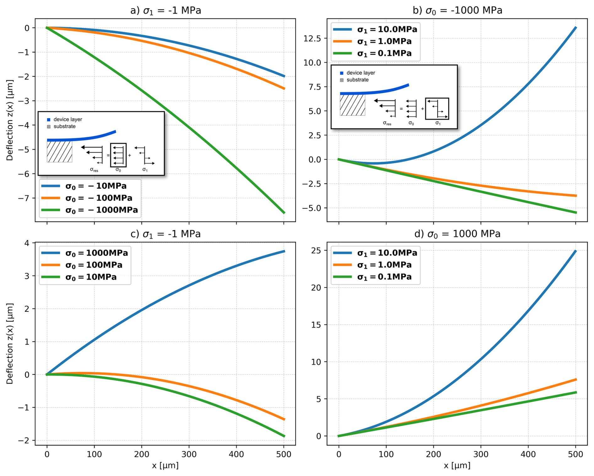
Figure 1Theoretically predicted tilt and curl deformations of a beam with h=1 µm, E=130 GPa, and ν=0.25.
Different silicon, 3C-SiC, and diamond device layers with various thicknesses, microstructures, and mechanical properties are investigated on phosphorus-doped 〈100〉-oriented silicon substrates covered with a wet thermal oxide, summarized in Table 1. The deposition of polycrystalline 3C-SiC is performed in an LPCVD system. An alternating supply deposition (ASD) working with alternating gas flows of propane and silane with intermediate pump-out times is utilized, as described in Moll et al. (2024). Polycrystalline diamond (PCD) thin films from CarbonCompetence GmbH are fabricated in an HFCVD system at elevated temperatures from methane and hydrogen as precursor gases. For deposition of the PCD films with grains of several micrometers in diameter (m-PCD) and PCD films with small grains in the range of several nanometers (n-PCD), the temperature of the Si substrate was set to 800–850 °C and a total gas pressure of 5 mbar was applied, while the filament-to-substrate distance was maintained at 50 mm. The applied gas flows for the deposition of m-PCD and n-PCD films are set to CH4 H2 ratios of 0.1% and 2%, respectively. Further details on the deposition parameters can be found in Meindlhumer et al. (2024) and Huber et al. (2024). The grown thin films are benchmarked with single-crystalline silicon (SCSi) from a commercially available SOI wafer and with polycrystalline silicon (PCSi), as these are standard materials for MEMS devices. Two depositions of PCSi in an LPVCD system are performed at different temperatures, leading to very small nanosized silicon grains (s-PCSi) at a deposition temperature of 568 °C and larger grains by 2 orders of magnitude (l-PCSi) at a deposition temperature of 600 °C.
Moll et al. (2024)
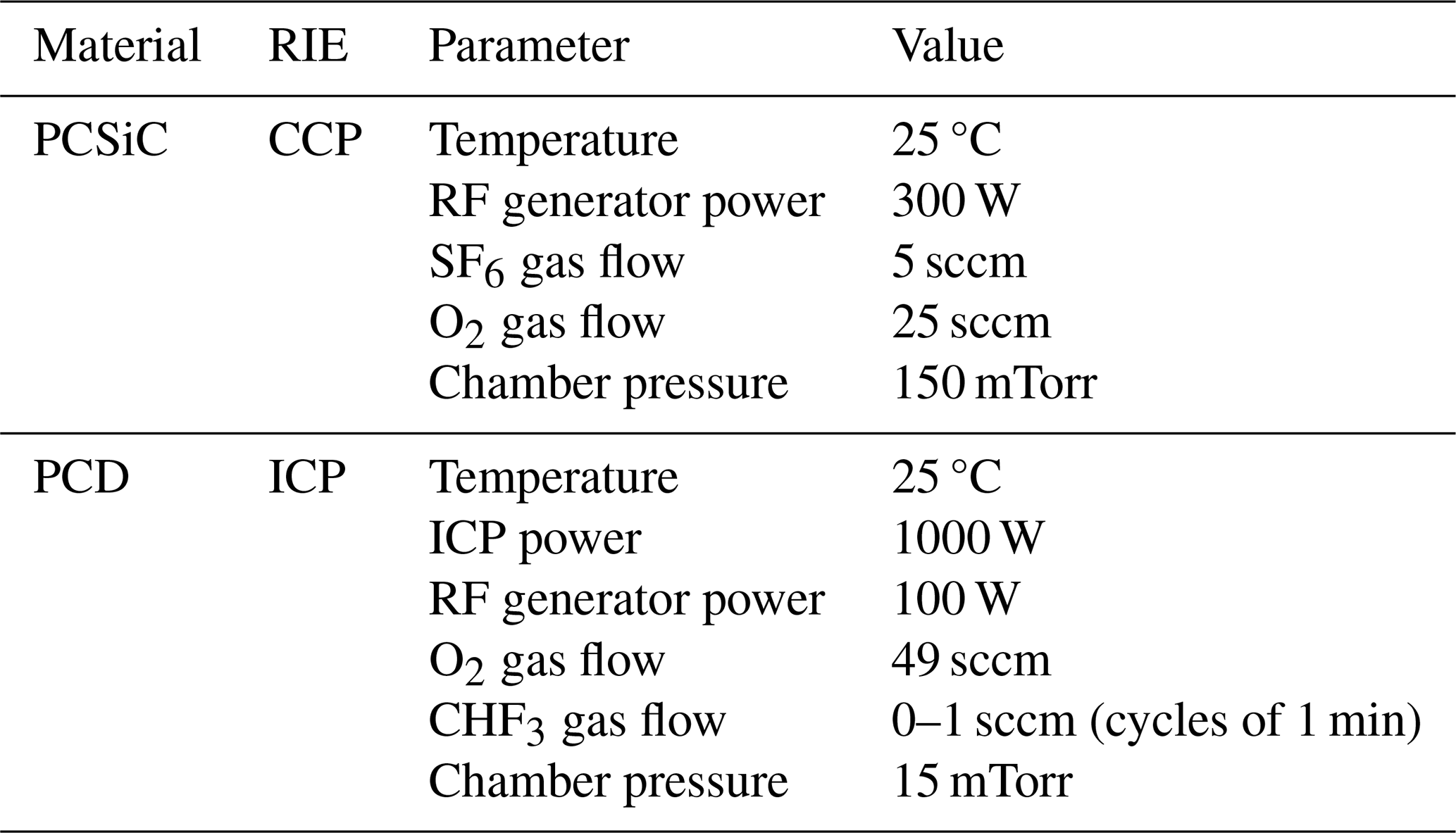
A Bosch process is used for micromachining single- and polycrystalline silicon. Furthermore, we developed suitable dry-etching recipes for PCSiC and PCD in a capacitively coupled plasma (CCP), STS RIE, and in an inductively coupled plasma reactive ion etcher (ICP RIE), Oxford Plasmalab 100, summarized in Table 2. We achieved an etching rate up to 100 nm min−1 for PCD and up to 150 nm min−1 for PCSiC, while for the selected etching parameters, the etch rate depends on the grain size of the polycrystalline device layer.
Test structures consisting of a cantilever and a step profile (SP) close to the anchor region are presented in Fig. 2a. The SP consists of 50 µm wide trenches etched through the device layer, down to the buried oxide. By utilizing the Bosch process, the cantilevers are released from the substrate, whereas the stress in the device layer leads to a static deflection. Cantilevers with a constant length of 500 µm and a width of 50 µm were fabricated to characterize the local stress distribution.
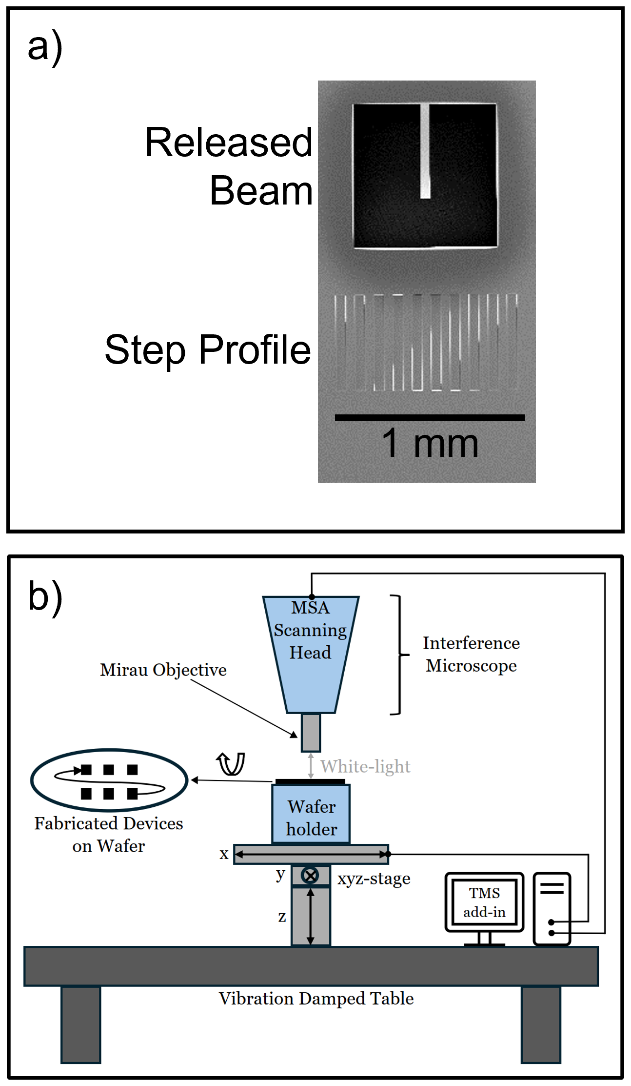
Figure 2(a) The automated contactless characterization of the local thin film thickness and stress uses a standard MEMS test structure with a cantilever and a step profile. (b) The WLI measurement setup consists of an MSA-400 equipped with a Mirau objective and an XYZ-stage.
A Micro System Analyzer (MSA-400) from Polytec GmbH, equipped with a 10 times magnifying Mirau objective and a piezoelectrically actuated stage, is used for static device characterization. An automated measurement setup is constructed to scan many devices fabricated on the same wafer at different positions for analyzing device layer thickness and film stress with WLI. To position the wafer below the objective, three motorized linear stages from Zaber Technologies Inc. are used both for the in-plane positioning and to focus on each device. A horizontal x-stage (X-LSM100A), a horizontal y-stage (X-LSM150A), and a vertical z-stage (X-VSR20A) with travel ranges of 100, 150, and 20 mm, respectively, are mounted on a vibration-damped table. Further on, each position stage, along with the MSA-400, is controlled with the same script to ensure an automated scan of all the devices at wafer level. A schematic representation of the measurement setup is shown in Fig. 2b.
From the three-dimensional scan of the SP, we extract an averaged profile line perpendicular to the etch trenches with several edges after the frontside etch, as shown in Fig. 3 for l-PCSi. In advance, leveling is performed, such that the upper plateaus of the SP are leveled out and set to 0. Even more, the leveling ensures that the maximum trench depth can be extracted accurately from the measurement data. A spatial step function zstep is designed to cover the specific shape of the trenches with rounded corners resulting from the dry-etching process:
The parameter s in Eq. (6) has the default settings su=10 if and sl=4 for the sharpness of the upper and lower edges, respectively. Additionally, f is the fixed spatial frequency of the trenches, z0 is the offset in height, and ϕ is the offset in the in-plane direction. Both the device layer thickness and the device height are determined as twice the amplitude A. The measurement is benchmarked with a stylus profilometer measurement, and very similar results are found. A similar approach is used for the extraction of the static deflection from the WLI scan of the cantilever. The plane correction is again done to minimize any impact from a tilted sample position, and the static deflection z(x) is fitted with Eq. (4). A representative measurement and fitting procedure is shown in Fig. 4, again for l-PCSi.
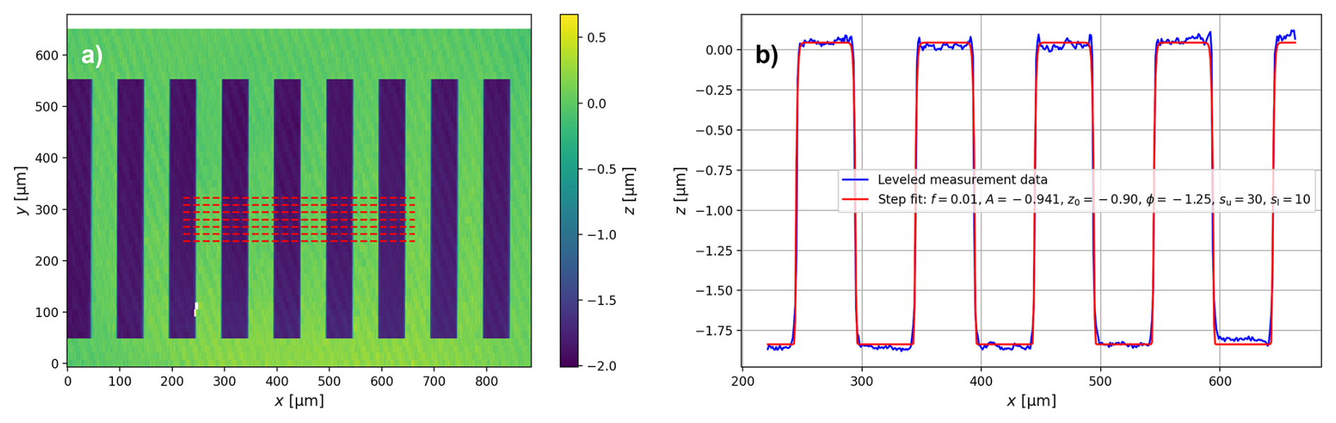
Figure 3(a) Typical leveled topography measurement of the step profile (SP) etched into the l-PCSi thin film. (b) Fit of Eq. (6) to the extracted average center line of the topography measurement.
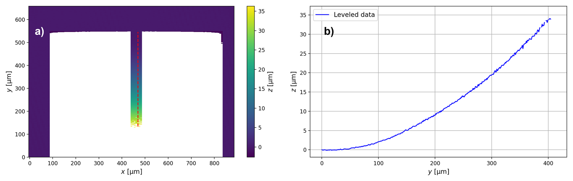
Figure 4(a) Typical leveled topography measurement of a l-PCSi beam. (b) Extracted deflection curve of the beam from the topography measurement.
Finally, we performed measurements of the wafer curvature with the l-PCSi, s-PCSi, and n-PCD thin films using an MX203-6-33 Wafer Geometry Gauge from E+H Metrology GmbH.
The material properties needed for the fitting procedures of the model by Fang and Wickert (1996) to the measured deflection curves of the cantilevers are summarized in Table 3. Standard values for SCSi are used from Hopcroft et al. (2010), while the Young's modulus of s-PCSi, l-PCSi, and PCSiC is calculated from the EB theory, the measured resonance frequency of the first EB mode, and the measured device layer thickness. We show the calculated stress distribution of the polycrystalline silicon device layer with small grains in the nanometer range (s-PCSi) for 40 devices with a length of 500 µm and a width of 50 µm in Fig. 5. The cantilever devices in each lower row are oriented parallel to the wafer flat, while the cantilever devices in each upper row are oriented perpendicular to the flat. Since the stress might not be isotropic, this approach allows us to distinguish between the stress values in two different directions (σ⟂ and σ∥) in close vicinity to minimize the impact of other parasitic effects, such as from microstructural variations. Results shown in the upper part of Fig. 5 represent the calculated mean stress σ0. We find compressive stress in most of the parallel devices and tensile stress in the perpendicular devices, with a huge difference in their mean values ( and ) of about 1542 MPa. However, the lower part of Fig. 5 shows the calculated gradient stresses in both directions and gives their mean values across the wafer in parallel and perpendicular directions, and , respectively. For the gradient stresses, we find negative, hence compressive, stress all over the wafer and a rather small difference in the mean values from parallel to perpendicular devices of about 24 MPa.
(Meindlhumer et al., 2024)(Klein and Cardinale, 1993)(Hopcroft et al., 2010)(Hopcroft et al., 2010)(Hopcroft et al., 2010)(Hopcroft et al., 2010)(Huber et al., 2025a)(Jackson, 2005)Table 3Young's modulus E and Poisson's ratio ν of the thin films studied.
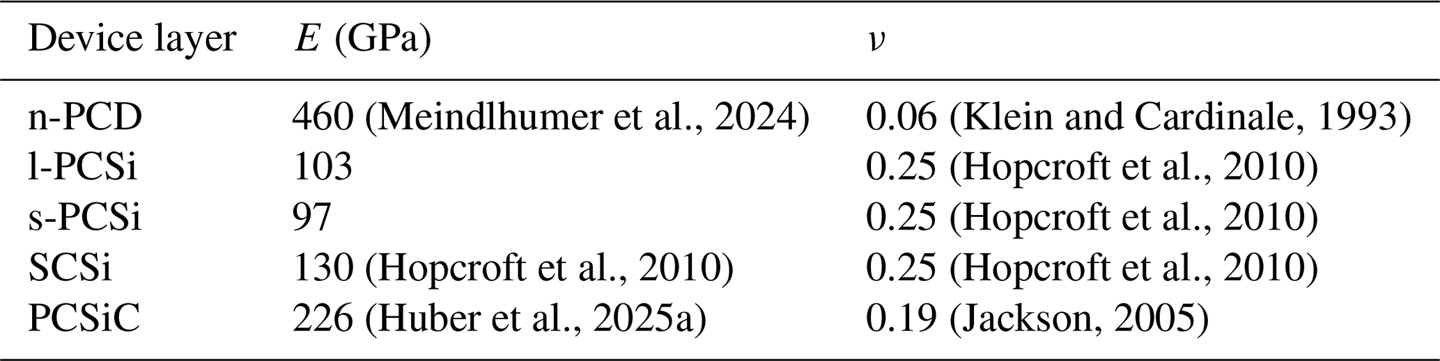
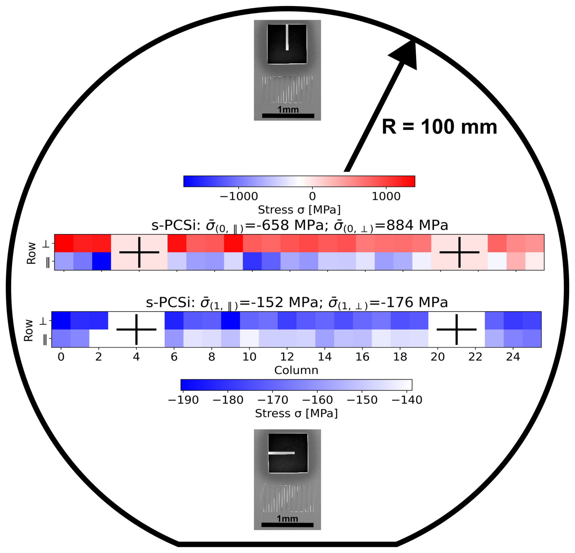
Figure 5Beams oriented parallel and perpendicular to the wafer flat are arranged in rows of 20 devices across the 4-inch (100 mm) wafer. For the presented data of s-PCSi, the local thickness is measured with the step profile (SP) and used to determine the mean stresses and (in the upper part of the figure) and the gradient stresses and (in the lower part of the figure). While for the gradient stresses all devices show negative (compressive) stresses, most of the devices parallel to the flat show negative mean stress, but all devices perpendicular to the flat show positive (tensile) .
We performed the same study of 40 devices for each of five different thin films (SCSi, s-PCSi, l-PCSi, n-PCD, and PCSiC) with WLI and the model from Fang and Wickert (1996) and summarized the results in Fig. 6. The data of the m-PCD film, however, were too noisy for WLI characterization, due to the rough surface of the device layer. The data are plotted per device, while every fit of the beam's deflection accounts for the local thickness of the device layer extracted from the measurement of the step profile. Furthermore, the data are separated into parallel and perpendicular devices and into gradient and mean stress. When focusing on the mean stress σ0 representing the tilt of the beams, we find a low tensile mean stress of 67 MPa in SCSi. A tensile but very high σ0 of 1650 MPa is also measured for PCSiC for both directions. Moderate absolute values of mean stress up to absolute values of 500 MPa can be found for n-PCD but by changing the sign from negative (compressive) to positive (tensile) from parallel to perpendicular. Similar behavior is present in l-PCSi (σ0-absolute values up to 600 MPa). A much larger change can be found for s-PCSi (σ0-absolute values up to 1700 MPa), as shown in Fig. 5. We find a very consistent trend for all device layers for σ1, independent of the orientation of the test structure. Since the thickness of the device layer changes from the center to the edge of the wafer, symmetric changes of σ1 can be found for n-PCD and PCSiC, while the silicon device layers show rather constant values. In particular, the SCSi device layer does not show any curl of the beams, resulting in σ1=0.
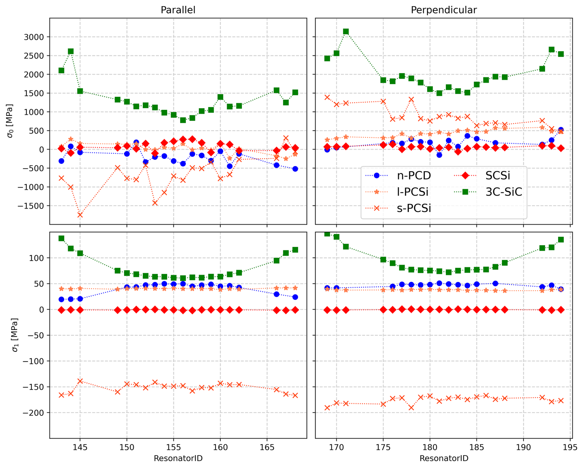
Figure 6The mean stress (in the upper half) and the gradient stress (in the lower half) are shown for parallel- and perpendicular-oriented devices, relative to the wafer flat. A total of 20 devices for each orientation are measured with a length of 500 µm and a width of 50 µm. While σ1 does not show any orientation dependence, the mean component of the stress changes from parallel to perpendicular for n-PCD, l-PCSi, and s-PCSi. The inserted lines serve as a visual guide.
A WLI measurement on a single device takes about 40 s, including the postprocessing steps. Repeated measurements are performed on the same device with ResonatorID = 182 on the l-PCSi wafer for 24 h. The gradient stress averaged for 210 measurements is calculated as MPa.
The direction-dependent mean stress σ0 measured for the polycrystalline silicon device layer with large grains in the range of ≈100 nm (l-PCSi), the polycrystalline silicon device layer with small grains in the nanometer range (s-PCSi), and the polycrystalline diamond device layer with small grains in the nanometer range (n-PCD) can be caused by several parameters during the deposition. Non-uniform temperatures in the CVD process, along with asymmetric gas flows, can lead to an anisotropic stress distribution in the wafer. Furthermore, the CTE is highly temperature-dependent, and even for SCSi and PCSi, the parameters differ by roughly a factor of 2 for different temperatures, as described by Mazur and Gasik (2009) for SCSi and by Tada et al. (2000) for PCSi-SiO2 stacks. The CTE is also dependent on the crystal orientation of the thin film, especially for SCSi, but also for PCSi, if there is a preferred growth direction. However, the identification of the microstructural origin of the direction-dependent stress is outside the scope of this work. Furthermore, the fitting procedure due to the leveling within the applied method is critical for the extraction of the correct mean stress, and the results shown for σ0 need to be used carefully, since small measurement and fitting uncertainties have a huge impact on σ0. A schematic is shown in Fig. 7, where the angle α represents the leveling error. The angle θ is the tilt of the beam at the anchor and is calculated as the sum of θ0 and θ1. Since θ1 is fixed by σ1 and the measured radius of the curvature R in Eq. (5), the leveling error in a measurement is directly added to θ0 and hence to σ0. An uncertainty of the leveling resulting in a device tilt α=1 mrad for a 2 µm thick beam leads to a variation in σ0 of 90.7 and 341 MPa for SCSi and n-PCD, respectively.
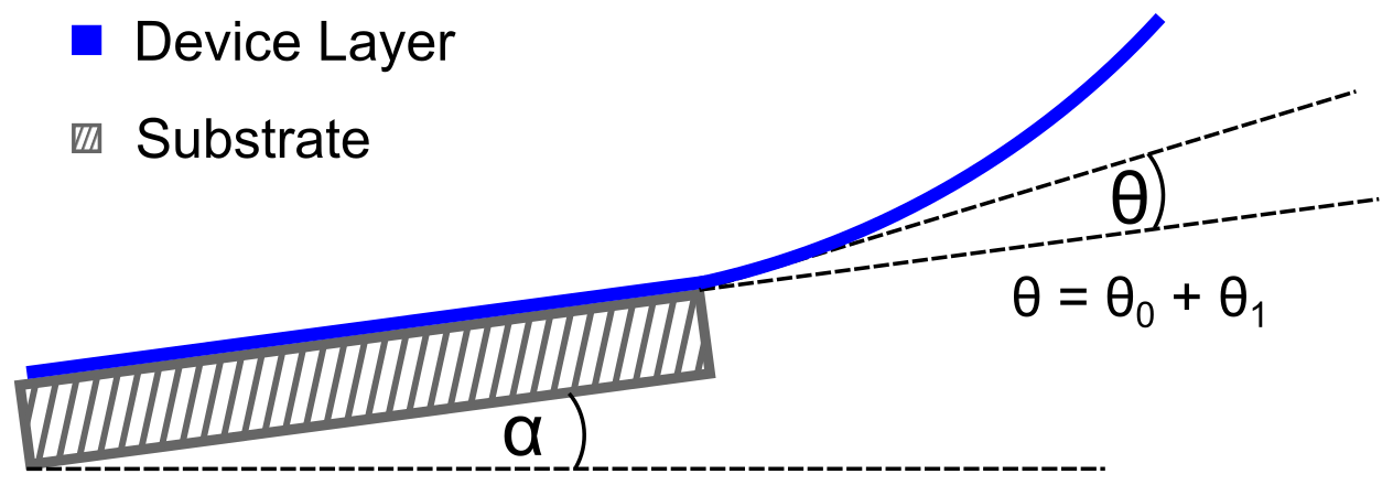
Figure 7Schematic representation of the impact of a device tilt α on the measured tilt of the beam at the anchor θ.
The calculation of the local device layer stress is done with precise knowledge of the thickness at each position. The presented structures are used to characterize six thin films with WLI. Hence, 182 devices fabricated on half of a 4-inch (100 mm) wafer are fully automatically measured to extract the local thickness and static deflection information. With this information, it is possible to map the local properties, as shown for the thickness in Fig. 8. The maps show different distributions of the device layer depending on whether its thickness is locally either thinner or thicker. Wafer bonding, as done for the fabrication of the single-crystalline silicon device layer within an SOI process, leads to a pattern originating from the subsequent grinding process to define the thin film thickness. The other device layers fabricated from CVD are showing more random patterns related to the gas flow in the CVD reactor and the relative positions of the gas inlets. However, we find the standard deviation of the thickness to be minimal for the PCSi wafers used, medium for the SCSi and the m-PCD device layers, and maximal for the n-PCD thin film, respectively. Regions of the PCSiC device layer were destroyed during device fabrication; hence, no thickness map is shown for this thin film.
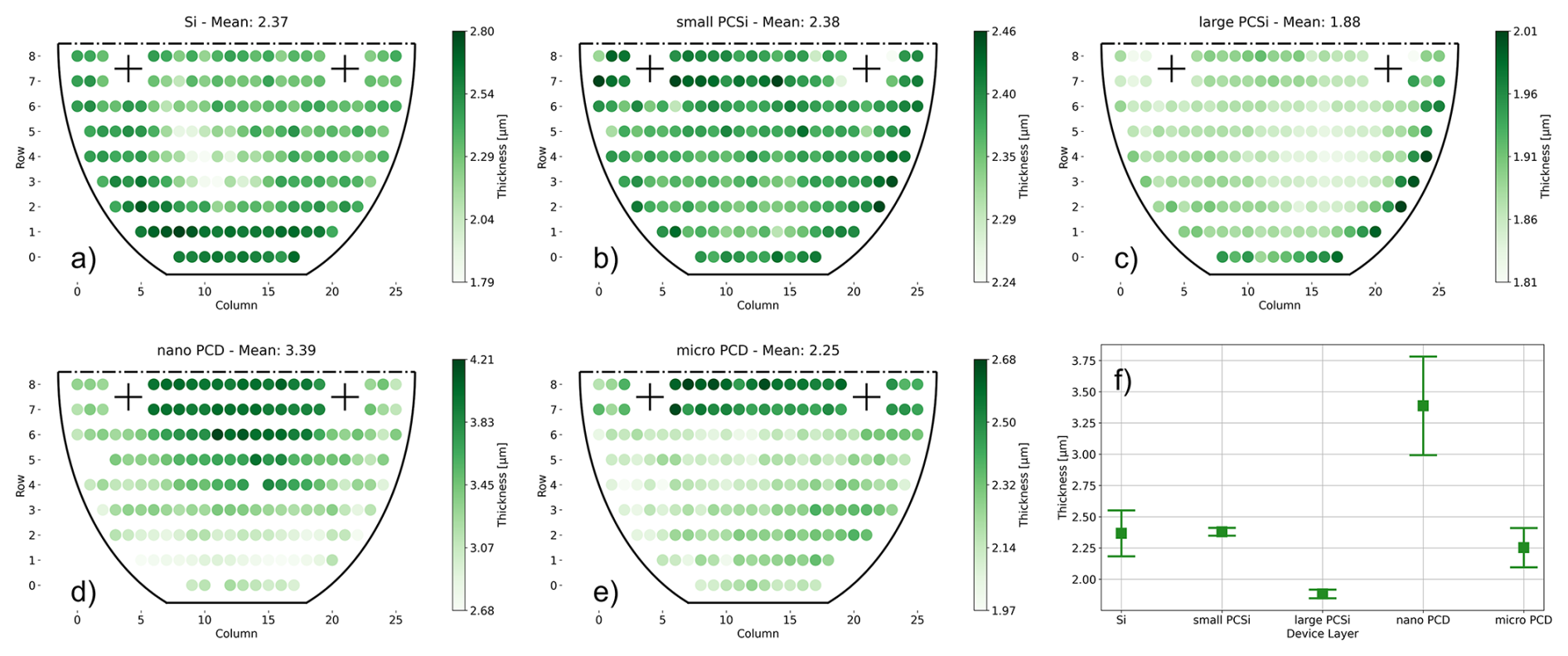
Figure 8Maps of 182 measurement points on half of a 4-inch (100 mm) wafer for (a) SCSi, (b) s-PCSi, (c) l-PCSi, (d) n-PCD, and (e) m-PCD. Their mean values and standard deviations are shown in panel (f).
As already mentioned, the extraction of σ1 from the measured curvature of the cantilevers leads to a symmetric result for parallel and perpendicular devices. For the gradient stress, the influence of the device tilt is irrelevant, and a closer look at the effect of the local thin film thickness on σ1 is done in Fig. 9. To do so, we calculated the average thin film thickness for the 40 studied devices per device layer and show the difference between the gradient stress calculated with the local thin film thickness hloc and the one with per device in both directions, parallel and perpendicular to the wafer flat. While the difference is below 10 MPa in most of the measurements, it reaches up to 38 MPa for PCSiC at the edge of the wafer, indicating the high precision of the presented combination of film thickness and film stress measurement.
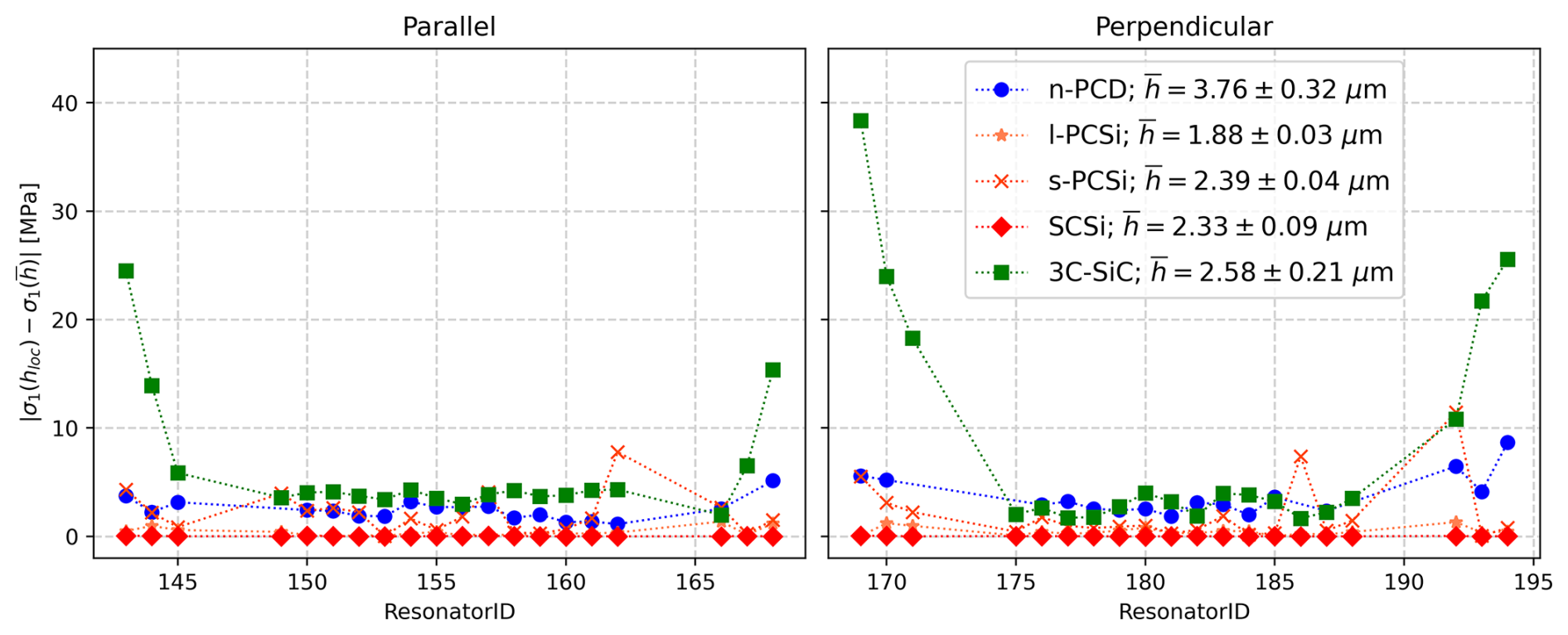
Figure 9Calculated differences between σ1 measured with the accurate local thin film thickness hloc and σ1 calculated with an averaged thickness
Stoney's equation, widely used to calculate the effective mean stress of a film from wafer curvature measurement techniques, is very convenient since it needs the thin film thickness h as the only thin film input parameter:
The radius R is measured optically or capacitively, and the properties of the substrate ES, νS, and hS (the Young's modulus, the Poisson ratio, and the thickness, respectively) are known. From considerations of the total force per unit width acting on the edge of the wafer f by Chason and Guduru (2016), one finds an expression for the so-called stress thickness
where fSurface and fInterface are additional forces related to the surface of the thin film and the interface between substrate and thin film. Expressing the effective mean stress from Eq. (8) and inserting Eq. (3) leads to depending only on the mean stress of the thin film, since the integral cancels out the stress gradient symmetric around the midplane of the thin film. Hence, it is clear that curvature measurements are only capable of measuring stress related to the mean stress in a thin film but cannot give any information on the gradient stress.
However, for the static deflection of MEMS devices, it is crucial to know both components to the residual stress. The list of three different MEMS cantilevers fabricated from l-PCSi, s-PCSi, and n-PCD in Fig. 10 compares the visible static deflection from the SEM image with the measured values of the effective mean stress from a capacitive wafer bow (WB) measurement and the mean values of and across 40 devices on each wafer, as described for Fig. 6. The l-PCSi cantilever shows an upwards static deflection, while the stress value from WB is negative. This discrepancy can be overcome by taking the positive into account. A situation like this is demonstrated in Fig. 1b, where the negative slope at the anchor and the superposition of the positive curl deflection lead to an overall positive deflection at the tip of the cantilever. Unfortunately, the measured value for this thin film does not fit the WB result due to possible limitations in the leveling procedure, also discussed above. Nevertheless, great accordance is found in the stress measurements for s-PCSi. For s-PCSi, the WB and the WLI values for are 115 and 113 MPa, while the averaged gives −164 MPa. These results describe a situation as shown in Fig. 1c. The static deflection of the s-PCSi cantilever shows a downwards bending with a rather high amplitude, as shown in the SEM image in Fig. 10. Finally, the n-PCD cantilever shows vanishing stress in the WB of 1 MPa, even though there is a slight static deflection visible in the SEM image of Fig. 10. The detailed analysis of the devices with WLI gives a rather high MPa, resulting from the small curvature and the high value of diamond's Young's modulus.
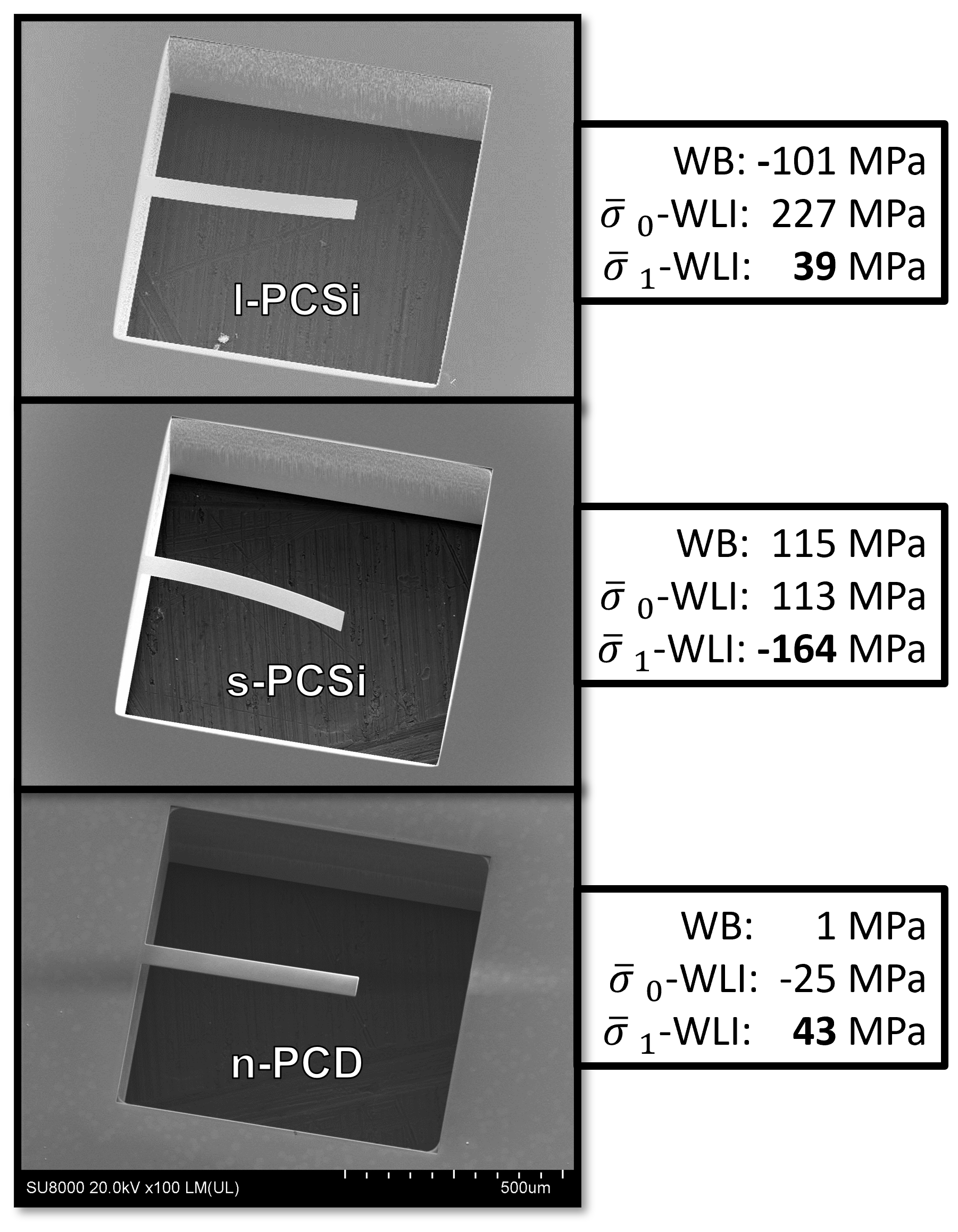
Figure 10SEM images of representative cantilevers from the l-PCSi, s-PCSi, and n-PCD thin films with the measured stress values from wafer bow (WB) and WLI techniques.
Further validation of the presented method is needed, since the gradient stress cannot be confirmed with wafer bow measurements. Possible alternatives to validate the results of this study are more elaborate techniques, like cross-sectional nanodiffraction XRD measurements (Keckes et al., 2012) or focused ion beam (FIB)-based methods. In the latter technique, a deformation analysis of a microstructure after sequential FIB-milling steps provides depth information on the stress in the studied film and hence the present stress gradient (Valente et al., 2005).
We present an MEMS test structure that is straightforward to fabricate with standard techniques of the MEMS industry in combination with an automated WLI measurement setup to determine local thin film thickness and film stress. The test structures are applied to six different device layers, revealing different thickness and static deflection distributions across the wafers. We calculate the local uniaxial mean stress σ0 and gradient stress σ1 following the FEM approach by Fang and Wickert (1996). This calculation is done by dividing the deflection into a tilt and curl component and performing a fit of a quadratic function to the extracted deflection curve. By scanning devices across the wafer automatically, we get stress and thickness values at different positions on the wafer and with the orientation of the cantilever parallel and perpendicular to the wafer flat. We find local variation in the stress due to the device layer deposition processes and demonstrate that for polycrystalline silicon and diamond device layers, an orientation dependence of the stress is present. Furthermore, we want to highlight the impact of the gradient stress on the curl deflection of the devices, resulting in large deflection amplitudes often hidden by measurements of the average residual stress with curvature measurement techniques. These findings illustrate the need for a detailed knowledge of the thin film properties for the fabrication of MEMS devices, as stress in the device layer affects the fabricated MEMS device in several ways.
As demonstrated, WLI can provide information, static deflection, and thickness in a contactless, fast, and automated way; hence, this technique can be used in both academia and industry for stress inspection. The precision of the measured mean stress can be further improved by scans of larger regions supported by the silicon frame, leading to a more effective leveling of the device. Furthermore, the approach by Fachin et al. (2011), combining WLI scans of single-side clamped cantilevers and double-side clamped bridges, is promising. The study of bridges allows the extraction of a parameter related to the clamping properties to distinguish between simply supported and fixed clamped bridges. However, the measurement of bridges is not capable of measuring tensile stresses, since no static deflection is present. Hence, the combined study of bridges and cantilevers overcomes the problem of leveling, since supported areas of the device on both ends of the bridges can be used, and additional information on the clamping properties can lead to an even higher precision of the measurement.
The computer code used is available on request from the corresponding author.
The data that support the findings of this study are available from the corresponding author upon reasonable request.
The conceptualization of the paper was done by DH, GP, and US. DH prepared the original draft, while GP and US did the supervision. CS built the software together with DH and AG. GP acquired the funding for the project and did the administration. Infrastructure and other resources were contributed by DS and US. Finally, investigations and visualizations were performed by DH and CS.
At least one of the (co-)authors is a member of the editorial board of Journal of Sensors and Sensor Systems. The peer-review process was guided by an independent editor, and the authors also have no other competing interests to declare.
Publisher's note: Copernicus Publications remains neutral with regard to jurisdictional claims made in the text, published maps, institutional affiliations, or any other geographical representation in this paper. The authors bear the ultimate responsibility for providing appropriate place names. Views expressed in the text are those of the authors and do not necessarily reflect the views of the publisher.
This article is part of the special issue “Sensors and Measurement Science International SMSI 2025”. It is a result of the 2025 Sensor and Measurement Science International (SMSI) Conference, Nuremberg, Germany, 6–8 May 2025.
This research has been supported by the Österreichische Forschungsförderungsgesellschaft (grant no. 888041).
This paper was edited by Sebastian Wood and reviewed by two anonymous referees.
Abadias, G., Chason, E., Keckes, J., Sebastiani, M., Thompson, G. B., Barthel, E., Doll, G. L., Murray, C. E., Stoessel, C. H., and Martinu, L.: Review Article: Stress in thin films and coatings: Current status, challenges, and prospects, J. Vacuum Sci. Technol. A, 36, https://doi.org/10.1116/1.5011790, 2018. a, b
Baryshev, S. V., Erck, R. A., Moore, J. F., Zinovev, A. V., Tripa, C. E., and Veryovkin, I. V.: Characterization of surface modifications by white light interferometry: applications in ion sputtering, laser ablation, and tribology experiments, J. Vis. Exp., e50260, https://doi.org/10.3791/50260, 2013. a
Bhatt, G., Manoharan, K., Chauhan, P. S., and Bhattacharya, S.: MEMS Sensors for Automotive Applications: A Review, Springer Singapore, Singapore, 223–239, ISBN 978-981-13-3290-6, https://doi.org/10.1007/978-981-13-3290-6_12, 2019. a
Boning, S. D. and Chung, E. J.: Statistical metrology: understanding spatial variation in semiconductor manufacturing, in: Proc. SPIE, vol. 2874, 16–26, https://doi.org/10.1117/12.250817, 1996. a
Bosseboeuf, A. and Petitgrand, S.: Application of microscopic interferometry techniques in the MEMS field, in: vol. 5145 of Optical Metrology, SPIE, https://doi.org/10.1117/12.500134, 2003. a
Brouzet, V., Gredy, V., Chenevas-Paule, F., Le-Chao, K., Guiheux, D., Laurent, A., Coutellier, V., and Le-Cunff, D.: Full Wafer Stress Metrology for Dielectric Film Characterization: Use Case, in: 2019 30th Annual SEMI Advanced Semiconductor Manufacturing Conference (ASMC), 1–7, ISBN 2376-6697, https://doi.org/10.1109/ASMC.2019.8791784, 2019. a
Chason, E. and Guduru, P. R.: Tutorial: Understanding residual stress in polycrystalline thin films through real-time measurements and physical models, J. Appl. Phys., 119, https://doi.org/10.1063/1.4949263, 2016. a, b
Chen, K.-S. and Ou, K.-S.: Chapter 17 – MEMS Residual Stress Characterization: Methodology and Perspective, William Andrew Publishing, Boston, 398–412, ISBN 978-0-323-29965-7, https://doi.org/10.1016/B978-0-323-29965-7.00017-8, 2015. a, b
Chircov, C. and Grumezescu, A. M.: Microelectromechanical Systems (MEMS) for Biomedical Applications, Micromachines, 13, 164, https://doi.org/10.3390/mi13020164, 2022. a
Conor, O., Martin, H., Magali, B., Russell, D., and Alan, M.: Characterization of micromechanical structures using white-light interferometry, Meas. Sci. Technol., 14, 1807, https://doi.org/10.1088/0957-0233/14/10/310, 2003. a
Cuthrell, R. E., Mattox, D. M., Peeples, C. R., Dreike, P. L., and Lamppa, K. P.: Residual stress anisotropy, stress control, and resistivity in post cathode magnetron sputter deposited molybdenum films, J. Vacuum Sci. Technol. A, 6, 2914–2920, https://doi.org/10.1116/1.575451, 1988. a
De Wolf, I.: Micro-Raman spectroscopy to study local mechanical stress in silicon integrated circuits, Semiconduct. Sci. Technol., 11, 139, https://doi.org/10.1088/0268-1242/11/2/001, 1996. a
Fachin, F., Nikles, S. A., Dugundji, J., and Wardle, B. L.: Analytical extraction of residual stresses and gradients in MEMS structures with application to CMOS-layered materials, J. Micromech. Microeng., 21, 095017, https://doi.org/10.1088/0960-1317/21/9/095017, 2011. a
Fang, W. and Wickert, J. A.: Determining mean and gradient residual stresses in thin films using micromachined cantilevers, J. Micromech. Microeng., 6, 301, https://doi.org/10.1088/0960-1317/6/3/002, 1996. a, b, c, d, e, f, g
Gennat, M., Meinig, M., Shaporin, A., Kurth, S., Rembe, C., and Tibken, B.: Determination of Parameters With Uncertainties for Quality Control in MEMS Fabrication, J. Microelectromech. Syst., 22, 613–624, https://doi.org/10.1109/JMEMS.2012.2236076, 2013. a
Genzel, C., Denks, I. A., and Klaus, M.: Residual Stress Analysis by X-Ray Diffraction Methods, Wiley-VCH Verlag & Co. KGaA, 127–154, https://doi.org/10.1002/9783527649884.ch5, 2012. a
Guckel, H., Burns, D., Rutigliano, C., Lovell, E., and Choi, B.: Diagnostic microstructures for the measurement of intrinsic strain in thin films, J. Micromech. Microeng., 2, 86, https://doi.org/10.1088/0960-1317/2/2/004, 1992. a
Hopcroft, M. A., Nix, W. D., and Kenny, T. W.: What is the Young's Modulus of Silicon?, J. Microelectromech. Syst., 19, 229–238, https://doi.org/10.1109/JMEMS.2009.2039697, 2010. a, b, c, d, e
Huber, D., Platz, D., Gesing, A., Fulmek, P., Steinmüller-Nethl, D., Pfusterschmied, G., and Schmid, U.: Impact of Grain Size on The Q-Factor of Poly-Crystalline Diamond Mems Resonators, in: 2024 IEEE 37th International Conference on Micro Electro Mechanical Systems (MEMS), 915–918, ISBN 2160-1968, https://doi.org/10.1109/MEMS58180.2024.10439421, 2024. a
Huber, D., Jurekovic, P., Schallert, C., Pfusterschmied, G., and Schmid, U.: Impact of Nitrogen Doping on the Q-Factor of Polycrystalline 3C-SiC MEMS Resonators, in: Eurosensors 2025, AMA Service GmbH, 72–73, https://doi.org/10.5162/EUROSENSORS2025/M2.2.4, 2025a. a
Huber, D., Schneider, M., Fulmek, P., Pfusterschmied, G., and Schmid, U.: Tailored measurement setup for the contactless characterization of MEMS resonators at the wafer level, J. Sens. Sens. Syst., 14, 89–98, https://doi.org/10.5194/jsss-14-89-2025, 2025b. a
Huff, M.: Review Paper: Residual Stresses in Deposited Thin-Film Material Layers for Micro- and Nano-Systems Manufacturing, Micromachines, 13, 2084, https://doi.org/10.3390/mi13122084, 2022. a
Jackson, K. M.: Fracture strength, elastic modulus and Poisson's ratio of polycrystalline 3C thin-film silicon carbide found by microsample tensile testing, Sensors Actuat. A, 125, 34–40, https://doi.org/10.1016/j.sna.2004.10.008, 2005. a
Jensen, B., Bitsie, F., and de Boer, M.: Interferometric measurement for improved understanding of boundary effects in micromachined beams, in: vol. 3875 of Symposium on Micromachining and Microfabrication, SPIE, https://doi.org/10.1117/12.360480, 1999. a
Keckes, J., Bartosik, M., Daniel, R., Mitterer, C., Maier, G., Ecker, W., Vila-Comamala, J., David, C., Schoeder, S., and Burghammer, M.: X-ray nanodiffraction reveals strain and microstructure evolution in nanocrystalline thin films, Scripta Materialia, 67, 748–751, https://doi.org/10.1016/j.scriptamat.2012.07.034, 2012. a, b
Khoshnoud, F. and Silva, C. W. d.: Recent advances in MEMS sensor technology-mechanical applications, IEEE Instrum. Meas. Mag., 15, 14–24, https://doi.org/10.1109/MIM.2012.6174574, 2012. a
Klein, C. A. and Cardinale, G. F.: Young's modulus and Poisson's ratio of CVD diamond, Diamond Relat. Mater., 2, 918–923, https://doi.org/10.1016/0925-9635(93)90250-6, 1993. a
Kurmendra and Kumar, R.: A review on RF micro-electro-mechanical-systems (MEMS) switch for radio frequency applications, Microsyst. Technol., 27, 2525–2542, https://doi.org/10.1007/s00542-020-05025-y, 2021. a
Kurth, S., Mehner, J., Shaporin, A., Michael, S., Ebert, M., Dötzel, W., and Gessner, T.: Determination of dimensional parameters in MEMS components by vibration analyses, Proc. Conf. IMAC-XXV, 1364–1371, 2007. a
Lober, T. A., Huang, J., Schmidt, M. A., and Senturia, S. D.: Characterization of the mechanisms producing bending moments in polysilicon micro-cantilever beams by interferometric deflection measurements, in: IEEE Technical Digest on Solid-State Sensor and Actuator Workshop, 92–95, https://doi.org/10.1109/SOLSEN.1988.26441, 1988. a
Masters, N., de Boer, M., Jensen, B., Baker, M., Koester, D., Muhlstein, C., and Brown, S.: Side-by-Side Comparison of Passive MEMS Strain Test Structures under Residual Compression, in: vol. STP1413-EB, ASTM International, ISBN 978-0-8031-2889-7, https://doi.org/10.1520/stp10989s, 2001. a
Mazur, A. V. and Gasik, M. M.: Thermal expansion of silicon at temperatures up to 1100 °C, J. Mater. Process. Technol., 209, 723–727, https://doi.org/10.1016/j.jmatprotec.2008.02.041, 2009. a
Meindlhumer, M., Ziegelwanger, T., Grau, J., Sternschulte, H., Sztucki, M., Steinmüller-Nethl, D., and Keckes, J.: Micromechanical properties of micro- and nanocrystalline CVD diamond thin films with gradient microstructures and stresses, J. Vacuum Sci. Technol. A, 42, https://doi.org/10.1116/6.0003235, 2024. a, b
Moll, P., Pfusterschmied, G., Schwarz, S., Stöger-Pollach, M., and Schmid, U.: Impact of alternating precursor supply and gas flow on the LPCVD growth behavior of polycrystalline 3C-SiC thin films on Si, Sensors Actuat. A, 372, 115376, https://doi.org/10.1016/j.sna.2024.115376, 2024. a, b
Moll, P., Pfusterschmied, G., Schmid, B., Schwarz, S., Artner, W., and Schmid, U.: Ultra-low CTE-mismatch of 3C-SiC-on-Si thin films for high temperature MEMS applications, Sensors Actuat. A, 384, 116262, https://doi.org/10.1016/j.sna.2025.116262, 2025. a
Osterberg, P. M. and Senturia, S. D.: M-TEST: A test chip for MEMS material property measurement using electrostatically actuated test structures, J. Microelectromech. Syst., 6, 107–118, https://doi.org/10.1109/84.585788, 1997. a
Small, M. K. and Nix, W. D.: Analysis of the accuracy of the bulge test in determining the mechanical properties of thin films, J. Mater. Res., 7, 1553–1563, https://doi.org/10.1557/JMR.1992.1553, 1992. a
Stoney, G. G. and Parsons, C. A.: The tension of metallic films deposited by electrolysis, P. Roy. Soc. Lond. A, 82, 172–175, https://doi.org/10.1098/rspa.1909.0021, 1909. a
Tada, H., Kumpel, A. E., Lathrop, R. E., Slanina, J. B., Nieva, P., Zavracky, P., Miaoulis, I. N., and Wong, P. Y.: Thermal expansion coefficient of polycrystalline silicon and silicon dioxide thin films at high temperatures, J. Appl. Phys., 87, 4189–4193, https://doi.org/10.1063/1.373050, 2000. a
Valente, T., Bartuli, C., Sebastiani, M., and Loreto, A.: Implementation and development of the incremental hole drilling method for the measurement of residual stress in thermal spray coatings, J. Therm. Spray Technol., 14, 462–470, https://doi.org/10.1361/105996305X76432, 2005. a, b